Note: Descriptions are shown in the official language in which they were submitted.
CA 02482025 2004-10-08
WO 03/086765 PCT/AU02/01168
SYMMETRICALLY ACTUATED INK EJECTION
COMPONENTS FOR AN INK JET PRINTHEAD CHIP
FIELD OF THE INVENTION
This invention relates to a printhead chip for an ink jet printhead. More
particularly,
this invention relates to a printhead chip that includes a plurality of
symmetrically actuated,
moving nozzle arrangements.
BACKGROUND OF THE INVENTION
As set out in the above referenced applications/patents, the Applicant has
spent a
substantial amount of time and effort in developing printheads that
incorporate micro
electro-mechanical system (MEMS) -based components to achieve the ejection of
ink
necessary for printing.
As a result of the Applicant's research and development, the Applicant has
been
able to develop printheads having one or more printhead chips that together
incorporate up
to 84 000 nozzle arrangements. The Applicant has also developed suitable
processor
technology that is capable of controlling operation of such printheads. In
particular, the
processor technology and the printheads are capable of cooperating to generate
resolutions
of 1600 dpi and higher in some cases. Examples of suitable processor
technology are
provided in the above referenced patent applications/patents.
The Applicant has overcome substantial difficulties in achieving the necessary
ink
flow and ink drop separation within the ink jet printheads.
As can be noted in the above referenced patents/patent applications, a number
of
printhead chips developed by the Applicant include a structure that defines an
ink ejection
port. The structure is displaceable with respect to the substrate to eject ink
from a nozzle
chamber. This is a result of the displacement of the structure reducing a
volume of ink
within the nozzle chamber. A particular difficulty with such a configuration
is achieving a
sufficient extent and speed of movement of the structure to achieve ink drop
ejection. On
the microscopic scale of the nozzle arrangements, this extent and speed of
movement can
be achieved to a large degree by ensuring that movement of the ink ejection
structure is as
efficient as possible.
The Applicant has conceived this invention to achieve such efficiency of
movement.
CA 02482025 2004-10-08
WO 03/086765 PCT/AU02/01168
2
SUMMARY OF THE INVENTION
According to the invention, there is provided a printhead chip for an ink jet
printhead, the printhead chip comprising
a substrate; and
a plurality of nozzle arrangements that are positioned on the substrate, each
nozzle
arrangement comprising
an active ink ejection structure that is positioned on the substrate and
spaced
from the substrate, the active ink ejection structure having a roof with an
ink
ejection port defined in the roof;
a static ink ejection structure positioned on the substrate, the active ink
ejection structure and the static ink ejection structure together defining a
nozzle
chamber in fluid communication with an ink supply, the active ink ejection
structure
being displaceable with respect to the static ink ejection structure towards
and away
from the substrate to reduce and increase a volume of the nozzle chamber to
eject an
ink drop from the nozzle chamber; and
at least two actuators that are operatively arranged with respect to the
active
ink ejection structure to displace the active ink ejection structure with
respect to the
static ink ejection structure towards and away from the substrate, the
actuators being
configured and connected to the active ink ejection structure to impart
substantially
rectilinear movement to the active ink ejection structure.
The invention is now described, by way of example, with reference to the
accompanying drawings. The following description is not intended to limit the
broad scope
of the above summary.
BRIEF DESCRIPTION OF THE DRAWINGS
In the drawings,
Figure 1 shows a three-dimensional view of a nozzle arrangement of a first
embodiment of a printhead chip in accordance with the invention, for an ink
jet printhead;
Figure 2 shows a three-dimensional sectioned view of the nozzle arrangement of
Figure 1;
Figure 3 shows a transverse cross sectional view of a thermal bend actuator of
the
nozzle arrangement of Figure 1;
CA 02482025 2004-10-08
WO 03/086765 PCT/AU02/01168
3
Figure 4 shows a three-dimensional sectioned view of the nozzle arrangement of
Figure 1, in an initial stage of ink drop ejection;
Figure 5 shows a three-dimensional sectioned view of the nozzle arrangement of
Figure 1, in a terminal stage of ink drop ejection;
Figure 6 shows a schematic view of one coupling structure of the nozzle
arrangement of Figure 1;
Figure 7 shows a schematic view of a part of the coupling structure attached
to an
active ink ejection structure of the nozzle arrangement, when the nozzle
arrangement is in a
quiescent condition;
Figure 8 shows the part of Figure 7 when the nozzle arrangement is in an
operative
condition;
Figure 9 shows an intermediate section of a connecting plate of the coupling
structure, when the nozzle arrangement is in a quiescent condition;
Figure 10 shows the intermediate section of Figure 9, when the nozzle
arrangement
is in an operative condition;
Figure 11 shows a schematic view of a part of the coupling structure attached
to a
connecting member of the nozzle arrangement when the nozzle arrangement is in
a
quiescent condition;
Figure 12 shows the part of Figure 11 when the nozzle arrangement is in an
operative condition; and
Figure 13 shows a plan view of a nozzle arrangement of a second embodiment of
a
printhead chip, in accordance with the invention, for an ink jet printhead.
DETAILED DESCRIPTION OF THE INVENTION
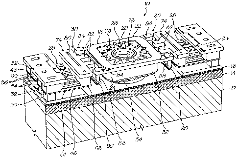
In Figures 1 to 5, reference numeral 10 generally indicates a nozzle
arrangement of
a printhead chip, in accordance with the invention, for an ink j et printhead.
The nozzle arrangement 10 is one of a plurality of such nozzle arrangements
formed
on a silicon wafer substrate 12 to define the printhead chip of the invention.
As set out in
the background of this specification, a single printhead can contain up to 84
000 such
nozzle arrangements. For the purposes of clarity and ease of description, only
one nozzle
arrangement is described. It is to be appreciated that a person of ordinary
skill in the field
can readily obtain the printhead chip by simply replicating the nozzle
arrangement 10 on
the wafer substrate 12.
CA 02482025 2004-10-08
WO 03/086765 PCT/AU02/01168
4
The printhead chip is the product of an integrated circuit fabrication
technique. In
particular, each nozzle arrangement 10 is the product of a MEMS - based
fabrication
technique. As is known, such a fabrication technique involves the deposition
of functional
layers and sacrificial layers of integrated circuit materials. The functional
layers are etched
to define various moving components and the sacrificial layers are etched away
to release
the components. As is known, such fabrication techniques generally involve the
replication
of a large number of similar components on a single wafer that is subsequently
diced to
separate the various components from each other. This reinforces the
submission that a
person of ordinary skill in the field can readily obtain the printhead chip of
this invention
by replicating the nozzle arrangement 10.
An electrical drive circuitry layer 14 is positioned on the silicon wafer
substrate 12.
The electrical drive circuitry layer 14 includes CMOS drive circuitry. The
particular
configuration of the CMOS drive circuitry is not important to this description
and has
therefore not been shown in any detail in the drawings. Suffice to say that it
is connected to
a suitable microprocessor and provides electrical current to the nozzle
arrangement 10 upon
receipt of an enabling signal from said suitable microprocessor. An example of
a suitable
microprocessor is described in the above referenced patents/patent
applications. It follows
that this level of detail will not be set out in this specification.
An ink passivation layer 16 is positioned on the drive circuitry layer 14. The
ink
passivation layer 16 can be of any suitable material, such as silicon nitride.
The nozzle arrangement 10 includes an ink inlet channel 18 that is one of a
plurality
of such ink inlet channels defined in the substrate 12.
The nozzle arrangement 10 includes an active ink ejection structure 20. The
active
ink ejection structure 20 has a roof 22 and sidewalls 24 that depend from the
roof 22. An
ink ejection port 26 is defined in the roof 22.
The active ink ejection structure 20 is connected to, and between, a pair of
thermal
bend actuators 28 with coupling structures 30 that are described in further
detail below. The
roof 22 is generally rectangular in plan and, more particularly, can be square
in plan. This is
simply to facilitate connection of the actuators 28 to the roof 22 and is not
critical. For
example, in the event that three actuators are provided, the roof 22 could be
generally
triangular in plan. There may thus be other shapes that are suitable.
The active ink ejection structure 20 is connected between the thermal bend
actuators
28 so that a free edge 32 of the sidewalls 24 is spaced from the ink
passivation layer 16. It
CA 02482025 2004-10-08
WO 03/086765 PCT/AU02/01168
will be appreciated that the sidewalls 24 bound a region between the roof 22
and the
substrate 12.
The roof 22 is generally planar, but defines a nozzle rim 76 that bounds the
ink
ejection port 26. The roof 22 also defines a recess 78 positioned about the
nozzle rim 76
which serves to inhibit ink spread in case of ink wetting beyond the nozzle
rim 76.
The nozzle arrangement 10 includes a static ink ejection structure 34 that
extends
from the substrate 12 towards the roof 22 and into the region bounded by the
sidewalls 24.
The static ink ejection structure 34 and the active ink ejection structure 20
together define a
nozzle chamber 42 in fluid communication with an opening 38 of the ink inlet
channel 18.
The static ink ejection structure 34 has a wall portion 36 that bounds an
opening 38 of the
ink inlet channel 18. An ink displacement formation 40 is positioned on the
wall portion 36
and defines an ink displacement area that is sufficiently large so as to
facilitate ejection of
ink from the ink ejection port 26 when the active ink displacement structure
20 is displaced
towards the substrate 12. The opening 38 is substantially aligned with the ink
ejection port
26.
The thermal bend actuators 28 are substantially identical. It follows that,
provided a
similar driving signal is supplied to each thermal bend actuator 28, the
thermal bend
actuators 28 each produce substantially the same force on the active ink
ejection structure
20.
In Figure 3 there is shown the thermal bend actuator 28 in further detail. The
thermal bend actuator 28 includes an arm 44 that has a unitary structure. The
arm 44 is of
an electrically conductive material that has a coefficient of thermal
expansion which is such
that a suitable component of such material is capable of performing work, on a
MEMS
scale, upon expansion and contraction of the component when heated and
subsequently
cooled. The material can be one of many. However, it is desirable that the
material has a
Young's Modulus that is such that, when the component bends through
differential heating,
energy stored in the component is released when the component cools to assist
return of the
component to a starting condition. The Applicant has found that a suitable
material is
Titanium Aluminum Nitride (TiAlN). However, other conductive materials may
also be
suitable, depending on their respective coefficients of thermal expansion and
Young's
Modulus.
The arm 44 has a pair of outer passive portions 46 and a pair of inner active
portions
48. The outer passive portions 46 have passive anchors 50 that are each made
fast with the
CA 02482025 2004-10-08
WO 03/086765 PCT/AU02/01168
6
ink passivation layer 16 by a retaining structure 52 of successive layers of
titanium and
silicon dioxide or equivalent material.
The inner active portions 48 have active anchors 54 that are each made fast
with the
drive circuitry layer 14 and are electrically connected to the drive circuitry
layer 14. This is
also achieved with a retaining structure 56 of successive layers of titanium
and silicon
dioxide or equivalent material.
The arm 44 has a working end that is defined by a bridge portion 58 that
interconnects the portions 46, 48. It follows that, with the active anchors 54
connected to
suitable electrical contacts in the drive circuitry layer 14, the inner active
portions 48 define
an electrical circuit. Further, the portions 46, 48 have a suitable electrical
resistance so that
the inner active portions 48 are heated when a current from the CMOS drive
circuitry
passes through the inner active portions 48. It will be appreciated that
substantially no
current will pass through the outer passive portions 46 resulting in the
passive portions
heating to a significantly lesser extent than the inner active portions 48.
Thus, the inner
active portions 48 expand to a greater extent than the outer passive portions
46.
As can be seen in Figure 3, each outer passive portion 46 has a pair of outer
horizontally extending sections 60 and a central horizontally extending
section 62. The
central section 62 is connected to the outer sections 60 with a pair of
vertically extending
sections 64 so that the central section 62 is positioned intermediate the
substrate 12 and the
outer sections 60.
Each inner active portion 48 has a transverse profile that is effectively an
inverse of
the outer passive portions 46. Thus, outer sections 66 of the inner active
portions 48 are
generally coplanar with the outer sections 60 of the passive portions 46 and
are positioned
intermediate central sections 68 of the inner active portions 48 and the
substrate 12. It
follows that the inner active portions 48 define a volume that is positioned
further from the
substrate 12 than the outer passive portions 46. It will therefore be
appreciated that the
greater expansion of the inner active portions 48 results in the arm 44
bending towards the
substrate 12. This movement of the arms 44 is transferred to the active ink
ejection
structure 20 to displace the active ink ejection structure 20 towards the
substrate 12.
This bending of the arms 44 and subsequent displacement of the active ink
ejection
structure 20 towards the substrate 12 is indicated in Figure 4. The current
supplied by the
CMOS drive circuitry is such that an extent and speed of movement of the
active ink
displacement structure 20 causes the formation of an ink drop 70 outside of
the ink ejection
CA 02482025 2004-10-08
WO 03/086765 PCT/AU02/01168
7
port 26. When the current in the inner active portions 48 is discontinued, the
inner active
portions 48 cool, causing the arm 44 to return to a position shown in Figure
1. As discussed
above, the material of the arm 44 is such that a release of energy built up in
the passive
portions 46 assists the return of the arm 44 to its starting condition. In
particular, the arm 44
is configured so that the arm 44 returns to its starting position with
sufFcient speed to cause
separation of the ink drop 70 from ink 72 within the nozzle chamber 42.
On the macroscopic scale, it would be counter-intuitive to use heat expansion
and
contraction of material to achieve movement of a functional component.
However, the
Applicant has found that, on a microscopic scale, the movement resulting from
heat
expansion is fast enough to permit a functional component to perform work.
This is
particularly so when suitable materials, such as TiAIN are selected for the
functional
component.
One coupling structure 30 is mounted on each bridge portion 58. As set out
above,
the coupling structures 30 are positioned between respective thermal actuators
28 and the
roof 22. It will be appreciated that the bridge portion 58 of each thermal
actuator 28 traces
an arcuate path when the arm 44 is bent and straightened in the manner
described above.
Thus, the bridge portions 58 of the oppositely oriented actuators 28 tend to
move away
from each other when actuated, while the active ink ejection structure 20
maintains a
rectilinear path. It follows that the coupling structures 30 should
accommodate movement
in two axes, in order to function effectively.
Details of one of the coupling structures 30 are shown in Figures 6. It will
be
appreciated that the other coupling structure 30 is simply an inverse of that
shown in Figure
6. It follows that it is convenient to describe just one of the coupling
structures 30.
The coupling structure 30 includes a connecting member 74 that is positioned
on the
bridge portion 58 of the thermal actuator 28. The connecting member 74 has a
generally
planar surface 80 that is substantially coplanar with the roof 22 when the
nozzle
arrangement 10 is in a quiescent condition.
A pair of spaced proximal tongues 82 is positioned on the connecting member 74
to
extend towards the roof 22. Likewise, a pair of spaced distal tongues 84 is
positioned on the
roof 22 to extend towards the connecting member 74 so that the tongues 82, 84
overlap in a
common plane parallel to the substrate 12. The tongues 82 are interposed
between the
tongues 84.
CA 02482025 2004-10-08
WO 03/086765 PCT/AU02/01168
A rod 86 extends from each of the tongues 82 towards the substrate 12.
Likewise, a
rod 88 extends from each of the tongues 84 towards the substrate 12. The rods
86, 88 are
substantially identical. The connecting structure 30 includes a connecting
plate 90. The
plate 90 is interposed between the tongues 82, 84 and the substrate 12. The
plate 90
interconnects ends 92 of the rods 86, 88. Thus, the tongues 82, 84 are
connected to each
other with the rods 86, 88 and the connecting plate 90.
During fabrication of the nozzle arrangement 10, layers of material that are
deposited and subsequently etched include layers of TiAIN, titanium and
silicon dioxide.
Thus, the thermal actuators 28, the connecting plates 90 and the static ink
ejection structure
34 are of TiAlN. Further, both the retaining structures 52, 56, and the
connecting members
74 are composite, having a layer 94 of titanium and a layer 96 of silicon
dioxide positioned
on the layer 74. The layer 74 is shaped to nest with the bridge portion 58 of
the thermal
actuator 28. The rods 86, 88 and the sidewalls 24 are of titanium. The tongues
82, 84 and
the roof 22 are of silicon dioxide.
When the CMOS drive circuitry sets up a suitable current in the thermal bend
actuator 28, the connecting member 74 is driven in an arcuate path as
indicated with an
arrow 98 in Figure 6. This results in a thrust being exerted on the connecting
plate 90 by the
rods 86. One actuator 28 is positioned on each of a pair of opposed sides 100
of the roof 22
as described above. It follows that the downward thrust is transmitted to the
roof 22 such
that the roof 22 and the distal tongues 84 move on a rectilinear path towards
the substrate
12. The thrust is transmitted to the roof 22 with the rods 88 and the tongues
84.
The rods 86, 88 and the connecting plate 90 are dimensioned so that the rods
86, 88
and the connecting plate 90 can distort to accommodate relative displacement
of the roof 22
and the connecting member 74 when the roof 22 is displaced towards the
substrate 12
during the ejection of ink from the ink ejection port 26. The titanium of the
rods 86, 88 has
a Young's Modulus that is sufficient to allow the rods 86, 88 to return to a
straightened
condition when the roof 22 is displaced away from the ink ejection port 26.
The TiAIN of
the cbnnecting plate 90 also has a Young's Modulus that is sufficient to allow
the
connecting plate 90 to return to a starting condition when the roof 22 is
displaced away
from the ink ejection port 26. The manner in which the rods 86, 88 and the
connecting plate
90 are distorted is indicated in Figures 7 to 12.
For the sake of convenience, the substrate 12 is assumed to be horizontal so
that ink
drop ejection is in a vertical direction.
CA 02482025 2004-10-08
WO 03/086765 PCT/AU02/01168
9
As can be seen in Figures 11 and 12, when the thermal bend actuator 28
receives a
current from the CMOS drive circuitry, the connecting member 74 is driven
towards the
substrate 12 as set out above. This serves to displace the connecting plate 90
towards the
substrate 12. In turn, the connecting plate 90 draws the roof 22 towards the
substrate 12
with the rods 88. As described above, the displacement of the roof 22 is
rectilinear and
therefore vertical. It follows that displacement of the distal tongues 84 is
constrained on a
vertical path. However, displacement of the proximal tongues 82 is arcuate and
has both
vertical and horizontal components, the horizontal components being generally
away from
the roof 22. The distortion of the rods 86, 88 and the connecting plate 90
therefore
accommodates the horizontal component of movement of the proximal tongues 82.
In particular, the rods 86 bend and the connecting plate 90 rotates partially
as shown
in Figure 12. In this operative condition, the proximal tongues 82 are angled
with respect to
the substrate. This serves to accommodate the position of the proximal tongues
82. As set
out above, the distal tongues 84 remain in a rectilinear path as indicated by
an arrow 102 in
Figure 8. Thus, the rods 88 that bend as shown in Figure 8 as a result of a
torque
transmitted by the plate 90 resist the partial rotation of the connecting
plate 90. It will be
appreciated that an intermediate part 104 between each rod 86 and its adjacent
rod 88 is
also subjected to a partial rotation, although not to the same extent as the
part shown in
Figure 12. The part shown in Figure 8 is subjected to the least amount of
rotation due to the
fact that resistance to such rotation is greatest at the rods 88. It follows
that the connecting
plate 90 is partially twisted along its length to accommodate the different
extents of
rotation. This partial twisting allows the plate 90 to act as a torsional
spring thereby
facilitating separation of the ink drop 70 when the roof 22 is displaced away
from the
substrate 12.
At this point, it is to be understood that the tongues 82, 84, the rods 86, 88
and the
connecting plate 90 are all fast with each other so that relative movement of
these
components is not achieved by any relative sliding movement between these
components.
It follows that bending of the rods 86, 88 sets up three bend nodes in each of
the
rods 86, 88, since pivotal movement of the rods 86, 88 relative to the tongues
82, 84 is
inhibited. This enhances an operative resilience of the rods 86, 88 and
therefore also
facilitates separation of the ink drop 70 when the roof 22 is displaced away
from the
substrate 12.
CA 02482025 2004-10-08
WO 03/086765 PCT/AU02/01168
In Figure 13, reference numeral 110 generally indicates a nozzle arrangement
of a
second embodiment of a printhead chip, in accordance with the invention, for
an ink jet
printhead. With reference to Figures 1 to 12, like reference numerals refer to
like parts,
unless otherwise specified.
The nozzle arrangement 110 includes four symmetrically arranged thermal bend
actuators 28. Each thermal bend actuator 28 is connected to a respective side
112 of the
roof 22. The thermal bend actuators 28 are substantially identical to ensure
that the roof 22
is displaced in a rectilinear manner.
The static ink ejection structure 34 has an inner wall 116 and an outer wall
118 that
10 together define the wall portion 36. An inwardly directed ledge 114 is
positioned on the
inner wall 116 and extends into the nozzle chamber 42.
A sealing formation 120 is positioned on the outer wall 118 to extend
outwardly
from the wall portion 38. It follows that the sealing formation 120 and the
ledge 114 define
the ink displacement formation 40.
. The sealing formation 120 includes a re-entrant portion 122 that opens
towards the
substrate 12. A lip 124 is positioned on the re-entrant portion 122 to extend
horizontally
from the re-entrant portion 122. The sealing formation 120 and the sidewalk 24
are
configured so that, when the nozzle arrangement 10 is in a quiescent
condition, the lip 124
and a free edge 126 of the sidewalls 24 are in horizontal alignment with each
other. A
distance between the lip 124 and the free edge 126 is such that a meniscus is
defined
between the sealing formation 120 and the free edge 126 when the nozzle
chamber 42 is
filled with the ink 72. When the nozzle arrangement 10 is in an operative
condition, the free
edge 126 is interposed between the lip 124 and the substrate 12 and the
meniscus stretches
to accommodate this movement. It follows that when the chamber 42 is filled
with the ink
72, a fluidic seal is defined between the sealing formation 120 and the free
edge 126 of the
sidewalls 24.
The Applicant believes that the invention provides a means whereby
substantially
rectilinear movement of an ink-ejecting component can be achieved. The
Applicant has
found that this form of movement enhances efficiency of operation of the
nozzle
arrangement 10. Further, the rectilinear movement of the active ink ejection
structure 20
results in clean drop formation and separation, a characteristic that is the
primary goal of
ink jet printhead manufacturers.