Note: Descriptions are shown in the official language in which they were submitted.
CA 02482944 2004-10-18
WO 03/089784 PCT/US03/12057
M'ROVED MCU BASED HIGH ENERGY IGNITION
This application claims priority under USC 119(e) of provisional applications
Serial No.
60/374,019, filed Apri119, 2002; Serial No. 60/432,161, filed December 10,
2002; Serial No.
60/450,217, filed February 25, 2003.
FIELD OF THE INVENTION
This invention relates to an improved electronic coil-per-plug ignition system
for spark
ignition internal combustion (IC) engines, especially using higher energy
density coils with biasing
magnets, operating at higher battery voltage and current, used with improved
design capacitive
spark plugs with erosion resistant halo-disc type spark firing ends, with
improved suppression
1o inductors and spark plug wire, to accommodate high energy flow-coupled
ignition sparks, whose
operation is controlled using a micro-controller (MCU) to simplify the design
and improve the
control capabilities of the system, including being able to operate the
ignition without a phase or
cam reference signal. As a complete ignition system applied to any spark
ignition engine, it is
capable of improving its fuel ef$ciency and exhaust emissions, especially
under dilute mixture
conditions such as lean burn and high exhaust gas recirculation (EGR).
BACKGROUND OF THE INVENTION AND PRIOR ART
This invention relates, in part, to a 42 volt based coil-per-plug ignition
system as is
disclosed in my U. S. patent No. 6,142,130, referred to henceforth as ' 130,
to improve and simplify
its operation and versatility, including improving and simplifying its
electronic controls by use of
an MCU, raising the energy density of its open-E type coils through the use of
biasing magnets,
improving the housing design of the coils to eliminate cracking due to thermal
stresses, eliminating
the need for a variable control (saturable) inductor to limit the secondary
voltage upon switch
closure, and other related improvements. The invention also relates, in part,
to improving the
electromagnetic interference and end-effect aspects of the ignition system
disclosed in my U. S. patent
No. 6,545,415, referred to henceforth as '415. Other aspects of the invention
include improving the
design of capacitive type spark plugs capable of handling the higher spark
currents with reduced
erosion, and improved low resistance suppression spark plug wire. In a
preferred application, the
ignition is used with a 2-valve, 2-spark plug per cylinder engine with squish
flow, disclosed in my
U. S. patent No. 6,267,107 B l, referred to hence forth as ' 107, and
improvements of it filed in a
3 o patent application with the same filing date as the present one. The
disclosures of the above referenced
provisional patent applications, and the ' 130, '415, ' 107 patents cited
above, as well as those cited
below, are incorporated herein as though set out at length herein.
CA 02482944 2004-10-18
WO 03/089784 PCT/US03/12057
SLtI~IMARY OF INVENTION
This invention provides for an improved coil-per-plug ignition, as a complete
system including
ECU with micro-controller (MCU), ignitors, coils, spark plug wire, spark
plugs, and other
improved parts and features, which as a complete system is practical, low
cost, compact and
versatile, yet highly effective in providing flow-resistant ignition sparks
with high spark energy for
igniting lean and high EGR mixtures for better fuel efficiency with low
emissions.
The ignition system has an ECU with features disclosed in my patent ' 130 and
other improved
features as a result of the use of an MCU which takes over the functions of
creating the coil charging
control (dwell control) by internally creating a dwell or coil charging
period, which can be modified
by sensing the coil charging current or by sensing any other engine parameters
to control the coil
energy. As part of the coil charging control, the ignition features ignition
coil power switch enabling
circuitry which applies power to the coil power switches Swi (preferably
IGBTs) only during the coil
charging time. The MCU also provides the ability to find the firing cylinder
in a multi-cylinder engine
through coil sensing and control means, and can provide RPM limiting (REV
limiting), and other
ignition features by making use of the MCU, with the minimum number of
required electronic
components.
For conventional 12 volt battery systems, versus the emerging 42 volt systems,
the ECU
includes a step-up power converter and voltage regulator for raising the
voltage to a higher voltage,
typically in the range of 24 volts to 60 volts, and preferably 42 volts as
envisioned for the future.
2o The power converter is preferably of the simpler boost type converter,
versus the fly-back type
disclosed in my patent '130, which can be used with one additional low-cost
switch as a high
power bi-directional converter for also stepping down the voltage, for
example, from 42 volts to
14 volts as may be required in the future. A biasing magnet may be used in a
special design of this
converter, especially in the case of a high power bi-directional converter, to
reduce the size of the
magnetic core of the converter inductor.
Along.with the ECU, the ignition may include Ignitor units with multiple-coils
mounted
on a single block, or stand-alone coils with power switches and related
components mounted on a
circuit board on the back ofthe preferred low inductance E-core coils
disclosed in my patent ' 130 and
improved herein. These Ignitor units contain the ignition coil energizing and
firing power switches Swi
3o and their drivers and other components, including preferably the snubber
capacitors of a snubber
circuit disclosed in my patent ' 130. Alternatively, the snubber capacitors
may be placed in the ECU
with special ground return wiring to insure their proper operation. In the
case of stand-alone coils,
the capacitors are mounted on the circuit boards without use of the snubber
circuit, wherein the coil
leakage energy which is delivered to the capacitors is discharged across the
primary coil winding.
CA 02482944 2004-10-18
WO 03/089784 PCT/US03/12057
3
The ignition coils, of the low inductance open-E type disclosed in my patent
'130, are
improved by using biasing magnets to double their already high energy
densities, and making them
circularly symmetric so they can be mounted more reliably on, or near the
spark plugs, to be made
more universally applicable. In the preferred embodiment, one or two biasing
magnets are place
in the air-gaps at the end of the preferred open-E type cores. For a
cylindrical coil, an annular
biasing magnet is placed in the annular air gap at one end of the coil. In the
standard coil with
laminations making up a square or rectangular core, two opposing magnets are
paced in the air-
gaps at the open end of the E-core.
The coils are improved to handle some of the practical issues relating to the
wide
temperature variations found in an engine environment, which can crack the
coils in their epoxy
encapsulated form due to different expansions coefficients of the coil
constituents. In a preferred
embodiment, the coil housing is designed so that only the center leg of the
magnetic core is
inserted in the housing (the outer legs being outside of the housing and free
to make small sliding
motions), and is designed to be able to slide as the expansion and contraction
forces become high
(due to extremes in temperature), to thus prevent cracking. The large
temperature variations exist
since the coils are preferably mounted on the spark plugs, or near the spark
plugs.
Such very low inductance, inductive type coils can also be used in larger
format for
distributor type ignition systems, where the even shorter charge time Tch of
preferably about 250
micro-seconds (usecs) eliminates the need for providing conventional ignition
dwell, versus the
"charge-and-fire" dwell, or charge time Tch feature of the present invention.
The suppression spark plug wire and inductors, including miniature size
inductors and plug
wire which can be placed inside the special design spark plug andlor in the
high voltage towers of
the ignition coils, and/or in between, are a novel design using iron or steel
wire of high magnetic
permeability which is spiral wound in a small diameter to form an inductive
spark plug wire, or
inductor, to provide a skin depth about equal to or less than the wire radius
at about 1 MHz
frequency, to provide significantly higher resistance, i.e. about ten times or
more, above 1 MHz
over the DC resistance to reduce electromagnetic interference (EMI) and the
"end-effect" disclosed
in my U.S. patent '415. The spark plug wire and inductors are designed to have
a relatively lower
inductance so that the frequency associated with the discharge of the coil
output capacitance is
3o between 5 and 20 MHz so that the higher resistance of the wire of hundreds
of ohms or greater at
that frequency is more effective in damping the oscillations across the wire
and inductors and those
associated with the end-effect. The spark plug wires and inductors are steel
spiral over a magnetic
core made up of a combination of ferrite and powder iron, or iron particles of
the type used in
particle core, or any combination of these.
CA 02482944 2004-10-18
WO 03/089784 PCT/US03/12057
The spark plugs disclosed herein are preferably of a flow-coupling type
disclosed in my US
patents No. 5,517,961, No. 5,577,471 (referenced as '471), and ' 107 and are
of the capacitive type
disclosed in some detail in my US patents No. 5,315,982, and 4,774,914, which
are improved by
using metallization to provide high capacitance of 30 to 80 picoFarads (pF) in
a compact design,
with their electrodes made of erosion resistant material, such as tungsten-
nickel-iron or other
material, and with insulator preferably made of alumina strengthened with 20%
zirconia. The plugs
have an improved halo-disc type firing end disclosed in my patent '471,
designed for varying level
of spark gap penetration, and with a novel recessed insulator to reduce the
chances of inadvertent
interior firing while increasing the plug capacitance.
so OBJECTS OF THE INVENTION
It is a principal obj ect of the present invention to provide a coil-per-plug
ignition, as a
complete system including ECU with micro-controller to provide for a more
compact and versatile
system with ignitors that require fewer lower cost components, or stand-alone-
coils which are more
suitable for mounting on or near the spark plugs, and are more compact and
robust using biasing
magnets for more versatile mounting, and spark plug wire with better EMI
suppression capability
using steel wire, and spark plugs with high capacitance, low erosion and good
flow-coupling
capability, so that as a complete system the ignition is low-cost, easy to
manufacture, practical, and
compact, yet versatile and highly effective in providing flow-resistant
ignition sparks with high
spark energy for igniting lean and high EGR mixtures for better fuel
efficiency with low emissions.
Another object is to simplify and reduce the size of the power converter by
using a boost
type converter for the DC-DC converter with simple control features.
Another object is to use the MCU in conjunction with sensing signals from the
coils to
determine the firing order of the ignition without the need for a phasing or
cam signal.
Another object is to provide a housing design for the open-E type coil that is
more robust
under wide temperature variations by having the outer core section outside of
the coil housing.
Another object is to provide circularly symmetric, even smaller high energy
coils by using
biasing magnets so they can be mounted on or near the spark plugs, yet still
have high stored
energy of approximately 100 mini-Joules (mJ) or higher.
Another object is to provide a bi-directional converter based on a boost type
converter
which is simple, low-cost, compact, with special inductor winding so that
biasing magnets can be
used to halve the size of the magnetic core.
Other objects of the invention will be apparent from the following detailed
drawings of
preferred embodiments of the invention taken in conjunction with the
accompanying drawings.
CA 02482944 2004-10-18
WO 03/089784 PCT/US03/12057
BRIEF DESCRIPTION OF THE DRAWINGS
FIG. 1 is a partial circuit and partial block diagram of a preferred
embodiment of the coil-
per-plug ignition system showing one of several possible ignition coils with
their driving and
sensing circuits, which are shown controlled by an MCU, showing its various
connections in terms
of the special functions it performs.
FIG. 1 a is a detailed circuit drawing of the system of FIG. 1, excluding the
ignition coils
and their drivers and power switches which are shown in detail in FIG. 1.
FIGS. 2a to 2c are approximately to-scale drawings of the side, end and top
views of the
open-E type ignition coil with laminated core with the preferred feature of
having'the outer core
legs outside of the coil housing.
FIGS. 3a to 3c are approximately to-scale drawings of the open-E type ignition
coil with
laminated core with the outer core legs outside of the coil housing whose main
body is cylindrical in
shape, depicting two side views, one including a printed circuit board (PCB)
and component housing
mounted on its back, and an end view showing the structure on which is mounted
the PCB. FIG. 3 d
is a preferred circuit drawing of the parts (excluding the coil) that are
mountable on the PCB, which
is shown in FIG. 3e.
FIG. 4 is an approximately 1 '/2 times scale, partial side-view drawing of a
preferred open-
E type cylindrical coil with preferably laminated core. FIG. 4a is an
approximately 2 1/2 times
scale, partial side-view drawing of the top end of an ignition coil with a
biasing magnet located
within a slot cut in the core of the center leg at the top end. FIG. 4b is a
drawing of a coil similar
to FIG. 4a but with two biasing magnets located in slots cut out of each side
of the top end of the
core. FIG. 4c is a preferred bottom section of the coils of FIGS. 4a, 4b with
separate magnetic core
at the bottom for completing the magnetic path for favorable operation of the
biasing magnets.
FIGS. Sa, Sb and Sc are approximately to-scale, side view drawings of the low
inductance
ignition coils of the E-type and U-type, including biasing magnets which
present large air gaps for
the required low inductance, as well as allowing for smaller coil design for a
high stored energy
capability of approximately 180 millij oules (mJ) through the biasing action
of the magnets. FIG. Sd
is a partial side view drawing of a segmented secondary winding bobbin for
containing the magnets
of FIGS. Sa and Sb.
FIGS. 6a and 6b are approximately to-scale, side-view drawings of insulators
for capacitive spark
plugs for the preferable halo-disc plugs of FIGS. 6c, 6d, 6e, and 6f, made of
alumina or zirconia
strengthened alumina to give a higher dielectric constant, and with internal
and external metallized
surfaces for the capacitance, and with concave versus convex insulating ends
for larger diameter
center electrodes with a higher capacitance.
CA 02482944 2004-10-18
WO 03/089784 PCT/US03/12057
6
FIGS. 6c to 6e are approximately to-scale, side-views of capacitive, halo-disc
plugs
improved by using the insulators of FIGS. 6a, 6b, which accommodate larger
diameter, better heat
sinking center electrode at the bottom section of the plugs. FIGS. 6d and 6e
include suppression
inductors interior to the spark plug insulators. FIG. 6f is a twice-scale side
view drawing of the
spark plug shell ground firing end, excluding the center firing electrode,
showing more details of
the insulator and shell firing end.
FIG. 7a is a twice-scale, partial side view drawing with preferred dimensions
of the
magnetic core, secondary winding bobbin, and biasing magnets of FIG S b. FIG.
7b is a twice scale
partial side view of the preferred housing for the coil of FIG. 7a. FIG. 7c is
a twice-scale partial
1o top end view of a slice of the core of FIG. 7a depicting a preferred
rectangular laminated core.
FIG. 7d is an expanded view of a small section of FIG. 7c showing an inside
corner of the housing
and outer laminations.
FIGS. 8a and 8b are partial, expanded side view drawings of cores with spiral
windings making
up inductive spark plug wire and their EMI suppressing capabilities in terms
of the voltage swings
that occur across the inductive wire when placed between the high voltage
secondary winding of
the ignition coil and the spark plug high voltage electrode.
FIG. 9 is a partial circuit drawing of a simple form of high power bi-
directional converter
comprising a boost and buck converter, usable in automotive applications where
a dual voltage rail
is required. FIGS. 9a and 9b are the drive signals required to operate the
converter in boost (step-up
conversion) and buck (step-down conversion), and FIGS. 9c and 9d are the
associated currents
through the converter energy storage inductor.
FIG. 10 is a simple form of the buck switch S2 of the converter of FIG. 9.
FIG.11 is a novel form of the converter of FIG. 9 wherein a biasing magnet is
used in the
inductor made possible by using two identical windings on the core of the
converter inductor. FIG.
12 is a side view of one of many possible designs of the inductor of the
converter with biasing
magnet at the center air-gap of the core center leg.
CA 02482944 2004-10-18
WO 03/089784 PCT/US03/12057
DISCLOSURE OF PREFERRED EMBODIIvvIENTS
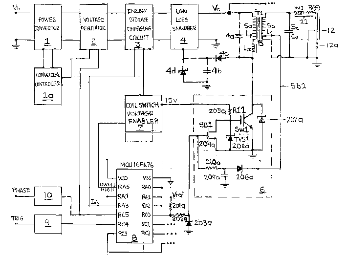
FIG. 1 is a partial circuit, partial block diagram of the coil-per-plug
ignition system made
up of power converter 1 and its controller 1 a; voltage regulator 2; energy
storage and coil charging
and current sensing circuit 3; low loss snubber circuit 4 fully disclosed in
my patent '130 and not
repeated here; one ignition coil 5 of several possible (also designated T1 of
Tn, or generically Ti);
coil driving and sensing circuit 6 shown as a dashed block containing the key
required components;
a coil switch voltage enabler 7 which supplies the coil power switches Swi
with power (15 volts
designated) during their turned on (coil charging) duration Tch. The coil
charging is controlled by
an MCU 8, in this case shown as a 16F676 with 8 A/D converter input/output
pins (RCO to RC3,
1o RAO to RA2, and RA4) for up to eight coils. Finally, there i~ the input
trigger circuit 9, and the
phase circuit 10 (a cam reference) available as an option to using coil
sensing by the MCU 8 to find
the firing cylinder. Blocks 1, 2, 3, 7, and 9 are shown in detailed circuit
form in FIG. la.
If the snubber circuit 4 is implemented, then the snubber capacitor is located
in the position
designated as 4b,along with isolation diode 4c and voltage clamp 4d, whose
operation is fully
disclosed in my patent '130. Otherwise, snubber capacitor is placed across the
primary winding
Sa of coil 5, designated as 4a in this case, and operates by having the coil
leakage Lpe energy
stored on it upon coil switch S 1 opening, discharged across the primary
winding to deliver part of
its energy to the coil secondary winding Sb and the spark, the rest of the
leakage energy being
dissipated in the coil windings and magnetic core.
Shown also in FIG. 1 is the coil 5 output capacitance Sc, of value Cs, which
is typically a
low capacitance of about 10 picoFarads (pF), the low value arising in part
that the coil high voltage
end is open, i.e. the magnetic core is open versus closed as in the standard
inductive coil. This
limits the high voltage capacitive energy discharged on spark firing to cause
EMI. That energy is
rapidly dissipated in the suppression spark plug wire or suppression inductor
11 with winding W 1
with frequency dependent resistance Rs(f) whose resistance R(f) increases with
frequency f, as
disclosed in my patent '415 and improved herein. At the high voltage end is
connected a preferably
capacitive spark plug 12 of capacitance Cpl of 30 to 80 pF, as will be further
disclosed. It has a
spark gap 12a which is preferably approximately 0.060" when used with normally
aspirated
engines with compression ratio below 12 to 1.
3o Note that the term "about" is taken to mean within ~ 50% of the quantity it
qualifies, i.e.
about 10 pF means within 5 pF and 15 pF. The term "approximately", as used
herein, is taken as
within ~ 20% of the quantity it qualifies, i.e. approximately 0.060" means
within 0.048" and
0.072".
CA 02482944 2004-10-18
WO 03/089784 PCT/US03/12057
Generically, the MCU performs several functions, the most important being
taking the
ignition firing trigger 9 and creating a charge time Tch (dwell) which is used
to charge each coil
sequentially, where the number of cylinders (assuming one coil per cylinder)
is programmed into
the MCU, so that once the proper firing sequence is determined, the charging
signal circulates from
pin RCO to pin RC3 (shown in this case for a 4-cylinder engine) with each
trigger signal. It is noted
that only one coil and associated circuit are shown here. The same circuits
apply to the other coils,
controlled by pins RCl to RC3, designated by ellipses.
In order to limit the size of the MCU, and the number of I/O pins, the pins
RCO to RC3, and
additionally RAO to RA2 and RA4 (for an ~-cylinder engine or a 4-cylinder with
two coils per cylinder)
are normally pulled high by pull-up resistors (201a shown in°this case)
to the reference voltage
(typically 5 volts). They are then connected via a current limiting resistor
202a to the gates of switch
driver N-type FET 204a (SD1 of SDn) whose gate is also connected to a 5 volt
Zener 203a
(corresponding to Vref). The drain of FET SD1 is pulled up to a higher voltage
(15 volts shown)
through slow-turn-on resistor 205a (R 11 ), sufficient to turn-on the power
switches Swl of Swn (IGBT
shown). The drains of FETs SDi are connected to the gates of their respective
IGBT power switches
Swi (drain of SDl connected to gate of Swl as shown).
A new feature is to use a large resistor for R 1 i, say 1 OK to SOK, depending
on the capacitance,
to slow the turn-on of the IGBT switches (which are preferable standard speed
type IGBTs). This
substantially reduces the voltage overshoot (voltage doubling) upon switch Swi
closure to eliminate
the need for the saturating inductor that is disclosed in my patent ' 130.
Transient voltage suppressor
(TVSi) diode 206a (TVS 1 ) is connected across the driver FET switch SDl for
protection of the driver
SD 1 and power switch Swl, as well as to provide additional capacitance to
slow down turn-on ofthe
power switches Swl, i.e. TVS diodes have a high intrinsic capacitance.
Otherwise, a separate
capacitor may be used, or the smaller intrinsic capacitance of the IGBT power
switches Swi my
perform the function of slow turn-on in conjunction with the resistors Rli.
The IGBTs Swi have
a diode or clamp 207i (207a shown) across them as required.
An advantage of the this MCU based ignition with A!D converters, is that the
MCU can be
used to find the firing cylinder (search mode) without a phase reference, by
bringing out a lead Sbi
(Sb 1 shown) from each coil that includes a few turns of the coil 5 secondary
winding Sb at the low
voltage end of the winding, e.g. that includes about 0.005 times the secondary
turns Ns, e.g. 20
turns for Ns equal to 4,000, and connecting the wire to a sensing circuit. The
sensing circuit in this
case is shown associated with MCU pin RCO comprising diode 20~a, capacitor
209a (e.g. 22
nanoFarad (nF)), and resistor 210a (e. g.100K) for pull-up resistor 201 a
approximately equal to 3 K.
The sensing circuit works by firing all the coils simultaneously during engine
cranking (MCU pins
RCO to RC3 go from output low (coil charging) to output high (spark firing),
to input for sensing
CA 02482944 2004-10-18
WO 03/089784 PCT/US03/12057
9
after the spark has fired and the capacitors 209i (209a shown) are fully
charged (initially negative
in this case for the typical coil negative high voltage, followed by a
positive voltage which can also
be used). With the above component values, the sense voltages range from 4.5
volts to just above
zero for -5 kV to -30 kV. The voltages on the pins are then A/D converted,
compared, and the
lowest voltage one designated the fired cylinder (highest cylinder pressure,
highest negative
voltage, and lowest positive sense voltage). For verification, the process can
be repeated to insure
that the next sense low is the expected one (next in the firing sequence). It
is noted that Pin RCS
can be used to lower the output voltage Vc, e.g. from 42 to 28 volts, to limit
to peak coil output
voltage upon switch Swi closure during cranking-and-sensing to prevent false
spark plug firing.
Pin RA3 is used to sense the coil charging current as °an override
protection in case the
current exceeds some threshold Ith, e.g. 36 amps for a normal 30 amps peak
current Ipk for a coil
primary inductance of approximately 330 microHenries (uH), i.e. for a typical
coil stored energy
of approximately 150 rnillijoules (mJ). This is achieved for a typical
preferred coil primary turns
Np equal to 50 and an open E-core cross-sectional area of approximately 1.0
square centimeter
(sq.cm) and approximately 0.6 sq.cm with biasing magnets, where "equal to"
means within ~ 10%
of the quantity it qualifies, i.e. Np between 45 and 55. For this preferred
embodiment, the coil
charge time Tc is approximately 0.3 milliseconds (msec). When the current
exceeds the threshold
current Ith, Pin RA3 goes low and terminates the MCU internally generated
dwell or charge time
Tch. During the cranking-and-sensing stage (search mode), the input RA3 is
disabled, since the
current will be approximately 2 '/2 times over the normal, e.g. 80 amps
instead of 30 amps, i.e. 4
times30 times (28/42) assuming Vc is 28 volts versus 42 volts at cranking.
If a phase 10 reference operation is preferred instead of the search mode,
this can be
accomplished by tying, for example, now undedicated Pin RCS to the phase
output, and sensing
for a low or high. It is noted that once the firing cylinder is sensed and the
engine is running, the
phase input is not required until the engine is stopped and restarted.
In the automotive application where 42 volts (or higher voltage) is available
for the present
higher voltage based ignition, a power converter may not be required. In that
case, switch Swl of
coil 5 (Tl ) preferably has a current sense resistor (48 of FIG. 9) between
the emitter of switch Swl
and ground, also acting as a fuse, connected to a sense circuit connected to
the MCU. In this case,
if a switch Swi should become disabled by shorting (the sense resistor/fuse is
opened), the other
coils will still function and the engine can still operate in a "limp mode".
FIG. 1 a is a detailed circuit drawing of the system of FIG. 1, excluding the
actual ignition
coil and its drivers and power switches, which are shown in detail in FIG. 1.
Also the sense circuits
are also not shown as they have been disclosed in FIG. 1.
CA 02482944 2004-10-18
WO 03/089784 PCT/US03/12057
In the present application, for the power converter 1 is shown a boost
converter comprised
of an input filter capacitor 18 connected to a voltage supply Vb, e. g. a car
battery, input over voltage
protection clamp 17, typically 30 volts, boost inductor 19 (of inductance Lb
of preferably about 40
uH), N-type FET switch 20, and boost output diode 21, which typically will be
a 60 volt Schottky.
5 Operation of this converter is well known to those versed in the art, and in
this application the
preferred frequency of operation is about 60 kHz, i.e. between 30 kHz and 90
KH?.
The converter controller drives switch 20 using the totem pole NPN and PNP
transistors
15a,15b, controlled by N-type FET 14 with pull-up resistorl4a, controlled by
output of comparator
91 which controls FET 14 through resistor 14b. Operation of this oscillator
controller circuit is
1o essentially identical to that of FIG.10 of my patent ' 130, and frost of
the component numerals of
that application, i.e. 87 to 97, correspond to those that have been used in
this drawing to designate
similar components and operation, i.e. resistors 87, 92a, 92b, 92c, 93, timing
capacitor 88, and
diode 89. In addition, there is included Zener 89a to reduce the switch 20 on-
time at high voltages,
e.g. Vcc of 20 volts. Optional N-type FET 90 is placed across timing capacitor
88 to disable it (turn
off power converter) during coil charging time Tch when Pin RA5 goes high
(during Tch).
Resistor divider 96a and 96b set the reference voltage of the regulator
comparator 97,
which in this case can be lowered during cranking to lower Vc to, say, 28
volts, if sensing is used.
This is done by having MCU Pin RC5 go high which turns on N-type FET 97b (with
base pull-up
resistor 97c) to place resistor 97a across resistor 96b, and lower the
reference voltage. The signal
2o to the inverting input of comparator 97 is taken from the regulator divider
31, 32.
Resistor 24b for charging timing capacitor 88, with associated components NPN
transistor
24 and resistor 24a control the peak current of the boost converter, where
transistor 24 senses the
converter output current flowing through energy capacitor 22, where the value
of resistor 24a is
typically at least 10 times greater than 23a, which may simply be a foil on
the circuit board of
resistance about 5 mini-ohms. For a 50 watt power converter operation,
preferred value for resistor
24a is approximately 0.15 ohms. Operation of this off time control is
disclosed in patent ' 130,
although the topology is different since this is a boost converter versus
flyback.
The purpose of the high current Schottky diode 23b, with negative temperature
coefficient,
is to allow sensing of both the capacitor charging and discharging current,
providing a voltage drop
on discharging, e.g. 0.5 volts at 30 amps, so that with resistor 23a sense NPN
transistor 23 (whose
collector is normally high via pull-up resistor 23c connected to regulator
voltage Vref) can perform
the coil charging control already mentioned. That is, the collector of sense
transistor 23 goes low
when the charging current exceeds a threshold, e. g. 36 amps, as would occur
if the coil secondary
output should fire during coil charging, to signal the MCU to terminate coil
charging. The collector
is shown connected to input pin RA3 of the MCU to provide the control feature.
CA 02482944 2004-10-18
WO 03/089784 PCT/US03/12057
11
A simple trigger input conditioning circuit is shown with its output connected
to Pin RC4
of the MCU. It is made of three resistors 221, 222, 224, a 5 volt Zener, and a
NPN transistor , with
output normally high, and the trigger signal to Pin RC4 being a pull to ground
whose duration is
less than Tch. Operation of this circuit is well known to those versed in the
art.
Shown also in FIG. 1 a is a circuit for providing the IGBT gate voltage Vg
(typically 12 to
volts) for the IGBT power switches Swi, in a controlled way. Shown is NPN
transistor switch
100 with its collector connected to resistor 99, e.g. 1K to 3.3K, which is
connected to the source
voltage Vc, and its emitter is connected to a parallel combination of
capacitor 101, of typical
capacitance 33 nF to 0.1 uF, and a Zener 102 which sets the gate voltage Vg.
Between point Vg
1o and base of transistor 100 is discharge diode 103 which is conilected to
both the drain of a control
N-type FET transistor 104, whose source is grounded, and to a resistor 105
(typically 22K) which
is connected to Vc. FET transistor 104 has its gate connected to a resistor
divider 106, 107, with
the gate terminal being the control terminal operated by N-type FET 109 which
is turned on during
the coil charge time (MCU Pin RAS goes high). Transistor 100 provides the IGBT
drive voltage
15 Vg, depending on whether transistor 109 (with pull-up resistor 109a) is on
or off. In this way, the
drive voltage to the gates of the power IGBT switches Swi can be enabled or
disabled by the MCU.
Preferably, when the reference voltage (5 volts shown) drops, to say 3.5 to
4.3 volts, as would
occur on engine turn-off, drive voltage Vg can be turned-off to prevent
uncertain firing of the
power switches Swi when the MCU goes into a low-voltage mode with uncertain
pin conditions.
2o In addition, the trigger signal Tr can be used to enable Vg during coil
charging (switch Swi on) and
to disable it when the switches are turned off. In this way, an MCU protection
override is provided
for the power switches Swi. Alternatively, in a passive mode where control is
not required for Vg,
transistor 100 is eliminated (shorted), the value of resistor 99 is increased,
and all the other
components are eliminated other than capacitor 101 and the Zener 102.
In FIG. la is also shown the pull-up resistors (block 201) of the MCU 8, and
the output
current limiting resistors 202a to 202d for the output control Pins RCO to
RC3. The MCU can also
run a 4-cylinder engine with two coils (and plugs) per cylinder, which can be
independently fired
by using the four extra MCU pins. Also shown are 12 volt regulator 85 and 5
volt regulator 86 and
its load capacitor 86a.
The MCU can perform many other functions, for example, increasing the coil and
spark
energy for a period of time after starting by increasing the coil charging
time, from say a nominal
180 mJ to 225 mJ, and then reducing the energy further to say 150 mJ when the
temperature rises
above a defined level by sensing, for example, the voltage across a
thermistor, as is known to those
versed in the art. It can also REV limit by simply putting in a delay after
ignition firing, e. g. 5 msec
for 6000 RPM for a 4-cylinder engine.
CA 02482944 2004-10-18
WO 03/089784 PCT/US03/12057
12
In the current application using preferably coils with open-E type magnetic
cores, as
disclosed in my patent '130, a preferred type of such coil with stored energy
capability in the 150
to 200 mJ range is shown in FIGS. 2a to 2c, which are approximately full
scale, depending on the
stored energy. FIG. 2a shows a partially detailed side view of such a
preferred coil, with E-core 110,
primary and secondary winding sections 111 and 112 respectively, with the
Ignitor unit 113
mounted on the back for mounting the power switch Swi and related components,
and a high
voltage tower 114. The coil and Ignitor may be mounted on an "L" bracket as
part of an assembly of
coils, as discussed, shown here as part 115, which can be metallic to ground
the core, or insulating,
with mounting holes 115a. The wires from the coils are indicated as 113 a,
which ideally emerge from
the coils as windings ends and are directly soldered onto the board within the
Ignitor housing 113.
A key feature of this variant of the E-core is that the laminations are mostly
outside the
housing 116, i. e. only the core center leg 110a, shown in the end-view FIG.
2b and top partial view
FIG. 2c, is within the housing, and it is designed so that it can move, i.e.
it is not firmly
encapsulated in the housing. The outer legs 1 lOb, FIG. 2c, are outside the
housing, as is the back
end 110c. In this way, with temperature variations, the laminations can move
relative to the
housing to minimize the chances of cracking. However, the laminations must be
held together to
the housing, which can be done with a flexible glue, e. g silicone, or by use
of a bracket 115 shown.
Preferably, the secondary winding 112 is segmented, with number of bays,
typically 6 to 10 bays.
FIG. 3a is an approximately to-scale side-view of an ignition coil of the type
of FIGS. 2a
through 2c, including the high voltage tower 61 which in an axial direction in
this case. The core
is of the preferred open-E type design whose center leg (not shown) is inside
the coil housing and
whose outer legs 55 are outside the housing. FIG. 3b is the back end view of
the coil of FIG. 3a
showing the clamping mount 62 with four mounting and clamping holes 63a to
63d, and the
primary wire ends, designated as Vc and -, and the secondary winding low
voltage winding wire
end designated as GND (for ground), with the opening 60b shown as a dashed
curve. In this case,
the possible sense winging is not shown. In this design, the housing 60 is
essentially cylindrical,
sealed at the high voltage end 60a and open at the low voltage end 60b into
which the windings,
bobbin and core center leg are inserted, and into which the encapsulant, e.g.
epoxy, is introduced.
FIG. 3c is an approximately to-scale, side-view of the ignition coil of FIG.
3a including a rear
housing 64 in which is a circuit board 65 on which are mounted the coil power
switch Swi and
driver components, and wherein the underside of the board is ground and is
clamped against the
end of magnetic core 50 to ground it and keep it firmly in the housing 60. The
board 65 and rear
housing 64 are clamped onto the coil housing clamping mount 62 against the
core end SOa (see
FIG.3b) by means of bolts 68a to 68d, which also serve for mounting the entire
coil unit to a frame.
CA 02482944 2004-10-18
WO 03/089784 PCT/US03/12057
13
FIG. 3d is a circuit diagram of parts, including power switch Swi, driver SDi
and resistor
R1 i, for mounting on the back of the ignition coil (FIG. 3c), with a
preferred circuit board 65 shown
in FIG. 3e, which includes snubber capacitors 82a, 82b which eliminate the
need for extra wire and
the snubber circuit (four wires shown on connector 67). In this design, with
reference to FIG.3d,
the snubber capacitor means Csn (82) is connected across the coil primary
winding designated as
an ideal transformer winding Lp (83a) with leakage inductor Lpe (83b). As
normal, upon ignition
firing, leakage current flows to the snubber capacitor 82, but in this case it
oscillates back through
the primary winding where it dissipates rapidly by delivering its energy to
the spark and to the
magnetic core and windings. In this way, the clamp Dswi (preferably internal)
across the switch
1o Swi does not have to dissipate power, and is only there to limit~open
circuit voltage.~Also, the EMI
is reduced in this design (versus with no snubber capacitor). With reference
to FIG. 3e, preferably
two parallel polyester high voltage capacitors are used. They can be located
across the board as
shown (82a, 82b), or if they are shorter, they can be placed across the board
(at right angles of
those shown), to provide more room for the section 66 where the drive
components are located.
FIG. 4 is an approximately 1'/2 times scale, partial side-view drawing of a
preferred form
of the open-E core type cylindrical ignition coil showing the magnetic core
with center leg 54,
outer legs 55, and back end 50, with the primary 53 and secondary 51 winding
sections, and an
electromagnetic interference (EMI) suppression inductor 70 within its high
voltage tower 61.
Preferably the windings and center leg are contained in an insulating cup 60
(not shown) With the
outer legs 55 of the magnetic core located outside the cup. Preferably the
magnetic core is made of
laminations, whose cross-section can be square or rectangular defining a close
to perfect cylindrical
coil housing 60 (not shown). For a rectangular cross-section of the magnetic
core, preferably the
ratio of the sides is approximately 1.3 in terms of the long side to the short
side to help achieve an
essentially cylindrical housing 60. For equal magnetic stressing of the outer
core legs 55 to the inner
core 54, the sum of the cross-sectional areas of the two outer legs should
equal 85% of the inner
leg 54, the 15% reduced factor coming from the reduced area of the center core
54 corners which
are preferably rounded by using narrower width laminations on the outside, and
from the fact that
some magnetic flux in the center leg will leak and not pass through the outer
legs 55.
The coil design shown is of particularly low inductance Lp, e.g. approximately
300 uH, with
3 o primary winding Np of approximately 50 turns, turns ratio Nt of
approximately 70, and bobbin 51 for
winding the secondary wire with preferably 9 bays, i.e. 8 to 10 bays, as
indicated in FIG. 7a. The
output capacitance Cs of this coil is reduced by having the primary winding 53
extending short ofthe
center leg core 54, e. g. approximately 80% of its length, and having the
secondary winding 52 in the
segmented bobbin 51 extend at or beyond the ends of the core center leg 54 and
outer leg 55. Coil
peak output voltages are typically 36 to 40 kV.
CA 02482944 2004-10-18
WO 03/089784 PCT/US03/12057
14
FIG. 4a is an approximately 2 I/2 times scale, partial side-view drawing of
the top end of an
ignition coil with a biasing magnet 69 located within a slot cut in the core
of the center leg at the
top end made up of transition section 112 and top section 50. FIG. 4b is a
drawing of a coil similar
to FIG. 4a but with two biasing magnets 69a and 69b located in slots cut out
of each side of the top
end of the core 50. FIG. 4c is a preferred bottom section of the coils of
FIGS. 4a and 4b, shown
associated with FIG. 4b in this case, which has a separate magnetic core 110
at the bottom end for
completing the magnetic path and for allowing favorable operation of the
biasing magnets. For the
preferred coil stored energy Ep of 100 mJ to 200 mJ, the preferred overall
dimensions of the
laminations are from equal to 1" across for a pencil type coil, to
approximately 1 1/4" across for
others. The length can vary from about 1 " to 2", or longer depending on
applic~tian.'Like numerals
represent like parts with respect to FIGS. 3a to 3c.
The design of the coil of FIG. 4a assumes the core to be made up of open-E
laminations
as per FIG. 3, except for the center leg 54 fanning out at the top to create
transitional section 112
above which a rectangular slot is cut of dimension just less than the maximum
width of the section
112, defining narrow channels 112a. The slot is for inserting the biasing
magnet 69. The two narrow
end sections 112a allows the laminations to maintain themselves as a single
structure, but forces
most ofthe magnetic flux lines 113 to pass through and along the complete
magnetic path or circuit,
versus short circuiting as flux line 114 which passes through the air-section
115 as flux leakage.
FIG. 4b represents a simpler form of open-E lamination where two biasing
magnets 69a
and 69b are placed vertically in the end section 50 symmetrically about the
middle. This is done
by cutting two rectangular vertical slots of height just short of the full
height of the end section 50
to accommodate the magnets 69a, 69b, creating narrow end sections 112b, which
as in FIG. 4a,
keeps the lamination as a single structure, but forces most of the magnetic
flux lines 113 to pass
through the along the complete magnetic path or circuit, versus short
circuiting as flux line 114 to
represent flux leakage. In this case, the top flux leakage section is width
"w"of the entire coil
lamination winding window. Like numerals represent like parts with respect to
the earlier figures.
Since the biasing magnets represent air-gaps of length "lm", it is not
practical to have an
open end at the bottom of the magnetic core, as in FIG. 3, since this will
lead to high magnetic flux
leakage of the biasing magnet and overly low coil primary inductance Lp. But
since we want to
maintain the advantages of using a single open-E core, separate magnetic core
sections 110 are
placed at the bottom as shown. These may introduce small air gaps lgl and Ig2,
as shown, but as
long as their sum is much less than the core window width "W ', i.e.
preferably less than half of
W, then the leakage will be small.
CA 02482944 2004-10-18
WO 03/089784 PCT/US03/12057
More generally, we can write:
W>2Elgi
where the sum is taken over all the air gaps in the magnetic path (excluding
the magnet). In
addition, we require for a low inductance coil that:
5 W ~ lm + ~ lgi
which resembles an open-E core in terms of the total air gap that an open-E
presents.
FIGS. Sa, Sb and Sc are approximately to-scale, side view drawings of the low
inductance
ignition coils of the open-E-type and IJ-type for an assumed approximately 150
mJ stored energy
r
(and scaled accordingly for lower or higher stored energy), using biasing
magnets to achieve the
10 very high energy density, which present large air gaps for the required low
inductance and high
energy density (mJ/gm). Like numerals represent like parts with respect to the
previous figures.
FIG. Sa is an open-E type coil of the pencil type, i.e. the magnetic core
length lc is
approximately twice or more than the core diameter of width Dc; and open-E
coil of FIG. Sb is a
cylindrical type coil where the length lc is less than twice the width
Dc.~Both coils (FIGS. Sa, Sb)
15 have biasing magnets 120 at the bottom open ends as shown, which are
preferably two separate
magnets for use with flat laminations. They can be a single ring type magnet
if the center leg is
essentially round, which can also be achieved with laminations whose center
legs 54 are of various
widths, preferably of three widths of the ratios 0.89, 0.72 and 0.44 of the
circle diameter, to
achieve a fill factor of over 80%, or of more widths.
For two separate magnets, the magnets would have a cross-sectional area Am (at
right
angles to the magnetization direction) 50% to 100% greater than the cross-
sectional areas of the
outer legs 55, assuming the use of high grade magnets with magnetic flux
densities of 1 Tesla or
higher and high coercive force, such as NdFeB or SmCo, and a magnetic length
lm to essentially
fill the end air gap (which equals the winding width W). However, if the
preferred cylindrical type
cup 60 (not shown) is used for the coil wherein the center leg 54 is in the
cup, and the outer legs
55 are outside the cup, then there will be a small air-gap lgl of about 0.050"
(depending on the
thickness of the cup wall adjacent to the magnet 120). A very small air gap
lg2 will also exist on
the inside to allow the center leg 54 (which is preferably wrapped with
insulation) to slide freely.
There are several advantages of this design, other than that of using the
biasing magnet to
achieve a higher magnetic swing up to twice normal. One is that the magnets do
not disturb the end
air-gaps used to achieve the preferred low inductance. Another is that the
magnets are separate
from the laminations, so that the do not interfere with the small sliding
movements of the core legs
allowed with temperature change to prevent cracking of the epoxy or other
material used to
CA 02482944 2004-10-18
WO 03/089784 PCT/US03/12057
16
encapsulate the windings. That is, the center leg 54 is wrapped with an
insulation, which is
encapsulated with the windings, but the center leg can slide inside the
insulation (along with the
outer legs 55 which are free to move) under thermal stress caused by differing
expansion
coefficients between the core material, the encapsulation, and the one or more
winding bobbins.
Another advantage is that the flux lines at the bottom of the core sections
54/55 tend to bend
towards the surface of the magnets 120 for less leakage flux.
In the design of FIG. 5a, the width Dc can equal 1" (0.9" to 1. l ") and the
length lc can be
approximately 2" for a stored energy of approximately 160 mJ. The narrower and
longer winding
window can be accommodated by using flattened (rectangular) magnet wire in a
free-standing
1o structure, i.e. without a bobbin, which is also preferred for other compact
coil structures. For
example, a primary winding equal to 50 turns (45 to 55 turns) of flattened
copper magnet wire of 20
AWG (American Wire Gauge) can be used with a winding length lp equal to 1.5"
and a wire
thickness of approximately 0.02"
In the design of FIG. 5b, the width Dc is approximately 1.3" and the length lc
is
approximately 1.6" for a stored energy of approximately 180 mJ. The window
width W is typically
up to 40% greater than the center leg 54 width, typically approximately 0.36";
the core cross-
section can be round, square, or rectangular with side ratios of approximately
1.3, as already
mentioned. Preferably, approximately 50 turns of wire (Np) in two layers are
used for the primary
winding 53, of winding length (lp) approximately 1". The magnetic flux swing
achievable through
2o the center leg 54 with the biasing magnets is approximately -1.6 Tesla to
approximately + 1.6 Tesla
to provide a high energy density.
FIG. 5c is a similar design as the E-cores but using an open-U core with open
end on the
bottom where a single biasing magnet 121 is used. All other things being
equal, the magnet cross-
sectional area Am is approximately twice the cross-sectional area of the two
legs 54, 55 (which are
approximately of equal cross-section). Also, as with the E-cores, the U-core
design preferably has
the windings 51/53 and the leg 54 about which the windings are wound in an
insulating cup (not
shown) with the outer leg 55 outside the cup. The leg 54 is preferably
insulated and free to slide
within the insulation with temperature change, as discussed with reference to
FIGS. 5a and 5b.
In all three cases, preferably approximately 50 turns oftwo layers of primary
wire are used,
3o typically 19 to 21 AWG, which are round but also can be flattened, for a
preferred primary
inductance of approximately 330 uH and peak primary current of approximately
32 amps, for coil
stored energy Ep of 100 mJ to 250 mJ for automotive applications. Typical
secondary to primary
turns ratio Nt is approximately 70 for use with 600 volt IGBTs, and
approximately 80 for use with
approximately 450 volt IGBTs.
CA 02482944 2004-10-18
WO 03/089784 PCT/US03/12057
17
FIG. 5d is a partial side view drawing of a segmented secondary winding bobbin
51 for
containing the magnets 120 of FIGS. 5a and 5b. Shown are the last three slots
52, as well as the
region 53 where the primary winding 53 locates and the magnetic core center
leg 54. As is seen,
two large interior slots 123 exist on the inside end of the bobbin where to
magnets 120 are inserted.
Since the magnets are located to repel each other they will stay in the slots
against their back wall
to allow the center leg 54 to slide freely past their inner face. The magnets
120 and slots 123 are
designed to produce minimum air gaps lgl and 1g2, typically 0.05" for lgl
taking the wall thickness
of the cup 60 into account, and about the same for 1g2. For the applications
of FIGS. 5a and 5b, the
magnet height "h" is approximately 0.20", its length lm is dictated by the
coil window width W,
and its other dimension made to conform to the size of the cord side, which
fog- a an approximately
coil stored energy of 150 mJ will typically range between 0.25" and 0.5",
depending on application.
While the preferred primary inductance Lp and peak primary current Ip are
approximately
300 uH and 32 amps, other values are possible using the designs of FIG. 4a to
5c which have large
air gaps (where the magnets are located). For example, assuming a primary
turns of 60 and a primary
winding length well short of the window length lw, e.g. for lw = 1.25", lp =
1.0", then a primary
inductance Lp of 500 uH is easily achievable, which taken with a peak primary
current of Ip of
amps provides a coil stored energy of 155 mJ, and for a turns ratio Nt of 70,
a peak spark
current of 350 ma, which is above the 200 ma required for ignition flow
coupling but produces less
spark plug erosion than the 450 ma spark current with the lower inductance
higher primary current
20 cases already discussed. Note that the inductance Lp not only depends
inversely on the winding
length lp, but on the length lp relative to the winding window length lw, i.
e. the smaller lp/lw, the
higher the inductance; it also depends on the location of the winding, which
preferably is located
against the back 50 of the core, i.e. for higher Lp and less magnetic fringing
fields beyond the open
bottom end. However, too short a length produces non-uniform magnetic stress.
25 FIGS. 6a and 6b are approximately to-scale, side-view drawings of
insulators for capacitive
spark plugs for the preferable halo-disc plugs of FIGS. 6c, 6d, 6e, and 6f,
made of alumina, or
zirconia strengthened alumina to give an approximately 50% higher dielectric
constant, and with
internal and external metallized surfaces for the capacitance. The two
insulators are identical
except for the length of metallization on the inside surface.
The length of the insulator "lins" is made up of three length sections 11,12,
13 of overall
length approximately 3.0 inches, l l defining the section along the threaded
shell section125 (FIG.
6c),12 defining the section along the non-threaded remaining shell section
188, and 13 defining the
top insulating tower section 185. The inner surface of the insulator of FIG.
6a is metallized ( 186a)
along the bottom length sections 11 and 12, i.e. along the entire metallic
section of the spark plug,
just short of the bottom end; the inner surface of the insulator of FIG. 6b is
metallized along its
CA 02482944 2004-10-18
WO 03/089784 PCT/US03/12057
18
entire length 186b as indicated, just short of the bottom end. In both cases,
the outside surface 187
is metallized along the length defined by I1 plus 12, the region where the
elongated outer metallic
shell case 188 is located, again just short of the bottom end. The insulator
thickness along lengths
11 and 12 are approximately 0.10", sufficient to withstand the high voltage
without puncturing, but
thin to give the maximum capacitance per unit length. The metallization of the
surfaces can be
done by various means, but is most readily and cheaply accomplished by a
chemical process where
copper is deposited by an electroless process after treatment, i. e. seeding
of the surfaces. Preferably,
the electrical contact between the outer metallization and the shell 188 is
made at the top end 188a
where the metallic shell is folded over the boss 193 to make a seal, and at
the section 188b where
the inner diameter of the shell has a step.
With reference to FIGS. 6a to 6f, a new feature of the insulators, designed
specifically for the
halo-disc'type plug which prefers the insulator end to be recessed below the
slots or cut-outs 126,
as per my US patent 5,577,471, ('471) is having a concave 187a, i.e. hollow,
versus convex end,
whose depth "lconc" (FIG. 6f) is such to prevent tracking, but not longer than
needed, e.g.
approximately 0.2". The advantage is that it allows for a larger diameter
center bore 127 for a large
bottom center "cooling" conductor 127a for better conducting heat away from
the center electrode
tip 128, and it allows for the building higher capacitance along the shell
threaded section 125 by
having a thinner insulator wall of approximately 0.10", as already mentioned.
The cooling
conductor diameter is between 0.12" and 0.18" for an interior shell diameter
"Dshell" between
0.35" and 0.4" for a~14 mm spark plug. Preferably, conductor 127a is of high
thermal conductivity
material such as copper or brass. Its erosion resistance is not important
since a center high voltage
erosion resistant electrode 129 will be attached directly to it, as in FIG.
6d, or with some kind of
fastener, e.g. nut 129a, which can also act to lock the center electrode 127a
into place with the
larger diameter end 130 working with it to create the lock.
FIG. 6c shows one version of the spark plug, where the bore 131 can be empty,
or filled,
for example, with powder to help make the seal of the center conductor. The
high voltage tip 132
can be soldered to the inner metallization (assuming the insulator of FIG. 6b
is used), or threaded
on as shown in FIGS. 6d, 6e (where the insulator inner diameter (ID) contains
a thread as shown).
An essentially cylindrical end electrode 128 is attached to a supporting
electrode 129 which is
welded or threaded (as shown) to the center conductor 127a. The insulator
upper outer diameter
(OD) preferably conforms to the standard 31/64" with the ID (bore) being
approximately 0.2"
smaller (of approximately 0.1" thick insulator).
If a slim-line plug is required, then the OD will be made smaller (with some
loss of
capacitance). However, as an option, one can have each of the OD and ID of the
entire insulator be
of one diameter along their outer and inner entire lengths, other than the
sealing boss 193, e.g. the
CA 02482944 2004-10-18
WO 03/089784 PCT/US03/12057
19
OD equal to 0.38" and the ID equal to 0.17". The inner seal can be made by
having the electrode
127a (which could now not have the larger diameter section 130) be of a
uniform diameter and
extend into section 13 where its would be thinned to, say, 0.1" to allow for a
powder seal, and
designed to contact the tip or nipple 132, with the nipple in turn making
electrical contact with the
inner metallization 186a. If the bore 131 ID can be made uniform, then the
inner metallization may
not be needed, with the capacitance formed between the extended length cooling
conductor 127a and
the uniform shell ID along 11 and 12. Or the electrode can be thinned along 12
and 13 and the bore
131 filled with conductive powder, e.g. brass, for both a seal and for
providing the capacitance.
FIG. 6d shows another version of the spark plug with the insulator of FIG. 6a,
where the center
1 o conductor 127a has an extension 127b over the length 12 around'which
powder can be filled to make
the seal, with an electric field diffuser 127c placed at the end of the inner
metallization 186a to
eliminate the effect ofthe sharp edge (and hence otherwise high electric
field). Between the diffuser
and the tip 132 is an EMI suppression element 70, which contacts the tip 132
by means of a spring
132a. The suppression element 70 can also be a length of the special spark
plug wire of FIG. 8b
contained in a semi-rigid structure which terminates at the diffuser 127c and
tip 132.
In place of the inner metallization 186a, or in conjunction with it,
conductive, e.g. brass,
powder can be placed around the cooling conductor extension 127b (along
section 12) and tamped to
make both the inner seal as well as the capacitance along that section 12.
Also, with reference to the
firing end electrode 129, which is shown without a fastener to attach it to
cooling electrode 127a, the
cooling of tip 128 can be further improved by having a copper core inside of
the end electrode 129.
This can be done by having the end electrode 129 and its tip 128 made up of a
shell or coating placed
over a small diameter, e.g. approximately 0.08", extension of the cooling
electrode 127a, for drawing
the heat even more e~ciently from the firing end 128, which produces the
hightemperature spark (arc
discharge) and is exposed to high temperature gases by preferably being placed
deeper into the
combustion chamber for better ignition flow coupling. Preferably, all the
surfaces of the cooling
electrode and its extension (particularly its extension) are covered to not be
directly exposed to the
spark and combustion gases. Finally, with respect to this figure, the absence
of a fastening unit 129a
reduces the chances of tracking and fouling of the surface of the inside of
the insulator 187a.
FIG. 6e is yet another version of the spark plug with integral suppression
spark plug wire 78,
where the spark plug wire is located in the insulator bore along its entire
length, shown making a
contact with the center conductor end section 130 (shown as a threaded
contact). The advantage of
this design is that it gives the maximum use of the plug bore length 12+13 for
the suppression spark
plug wire 78. The top fastening element 132b at the end is an electric field
diffuser (if insulator of
FIG. 6b is used) contacting the end of the metallization section, and also
serving to hold the spark plug
wire in place from moving. The spark plug wire 78 is clearly insulated from
the metallization 186b.
CA 02482944 2004-10-18
WO 03/089784 PCT/US03/12057
All three spark plugs of FIGS. 6c, 6d, 6e have some or all of the elements of
a halo-disc type
firing end structure disclosed in my U. S. patent 5,577,441, wherein the
ground electrode is made up
of a convex annular structure with slots 126 cut in them (shown in an expanded
view in FIG. 6f), to
provide a firing ring end 126a, into which may be located an erosion resistant
sub-ring 126b, such as
5 tungsten nickel iron, iridium, or other (or it may be a coating or plating
of erosion resistant material).
The center electrode 128 is preferably a cylindrical structure (FIGS. 6c, 6d)
located beyond
the ground ring 126, or inside the ring as in FIG. 6e. In order to insure
firing between the electrode
128 andthe ground ring 126a (or 126a/126b), the ID ofthe threaded shell
section 125 is the maximum
diameter Dshell that can be tolerated, preferably between 0.36" and 0.40",
without having too weak
10 a wall especially at its top junction which is stressed during Tightening.
In this way, assuming a
diameter equal to 0.10" for the electrode 129 and 0.38" for the shell ID along
the treaded section 125
(Dshell of FIG. 6), the clearance between the electrode 129 to the inner shell
wall is 0.14", or
approximately twice the preferred spark gap 128a of typically 0.06" to 0.08"
for normally aspirated
gasoline engines. If two plugs are used per cylinder, as per my patent ' 107,
one plug may have a large
15 gap, e. g. 0.08" for firing only under light load conditions, while the
other has a small gap, e. g. 0.04",
to handle the higher load conditions. For the large gap plug, it is even more
important to have the large
interior clearance to insure firing at the exterior spark gap 128a.
In addition, with reference to FIG. 6f (no central electrode shown), the
included angle ~ varies
to define the level of the spark gap extension by having the convex ground
section of length "lgnd"
2o be shorter or longer, the larger or smaller the angle respectively, varying
between 30° for a long
extension of plug firing end, and 90° for a short extension of firing
end. However, because of the flow-
coupling nature ofthe ignition, by definition, an extended gap type plug is
preferred (small angle ~).
The slot axial clearance also vary with the angle 8 (extension), typically
from 1/6" to 1/8", or
somewhat longer.
There are typically three or four slots cut around the annulus, four being the
preferred number
in this case for balancing the radial electric field to the posts that support
the ring 126a (see patent
5,577,471 ). The preferred length lgnd is approximately 0.2" and the angle is
approximately 40°. The
four slots are cut at every 90° preferably with a tapered cutter to
produce an inner post width equal
to the outer to avoid sharp interior points. Also, all inner metallic surfaces
are smoothed for reducing
electric field concentrations to prevent interior firing versus bring at the
spark gaps 128a,128b. The
concave insulator end 187b terminating near the inner edge of slots 126 has
side walls 187a that are
of a thickness to survive the harsh environment, but sufficiently thin to
accommodate a sealing nut
or other fastener if required, as indicated by 129a, which can seal the center
electrode 129 to the
cooling conductor 127a.
CA 02482944 2004-10-18
WO 03/089784 PCT/US03/12057
21
The high voltage electrode end 128 is made of erosion resistant material such
as tungsten-
nickel-iron, iridium or other, or a thick plating of such. The remaining
electrode 129 can be any used
in spark plugs, or of the same material as the tip. The plug capacitance Cpl
is preferably 30 to 60 pF,
defined mainly by the length of the shell spark plug shell 188 (including most
of the treaded section
125), thickness of the insulator, and its dielectric constant. The entire
spark plug end of center
conductor 129 and ground ring can be plated with catalyst material such as
palladium to enhance
combustion reactions.
While the emphasis of the above plug designs has been on the halo-disc type
plug end, the
capacitance nature of the plug can apply equally well to conventional plugs
with the long nose
1 o insulator at the firing end, with various electrode structures, incPuding
those disclosed elsewhere for
bring to the piston. In addition, the convex insulator end can be
conventional, or can be recessed if
used with the halo-disc design of my patent '471.
FIG. 7a is a twice-scale, partial side view drawing with preferred dimensions
of the magnetic
core, secondary winding bobbin, and biasing magnets ofFIG.S b. FIG. 7b is a
twice scale partial side
view of the preferred housing for the coil of FIG. 7a, rotated by 90°.
FIG. 7c is a twice-scale partial
top end view of a slice of the core of FIG. 7a depicting the preferred
rectangular laminated core
similar to FIG. 3a. FIG. 7d is an expanded view of a small section of FIG. 7c
showing an inside
corner of the housing and outer laminations. Like numerals represent like
parts with respect to
FIGS.3a to Sd.
In FIGS. 7a to 7c, the preferred dimensions are assumed to be X10%. FIG. 7a
shows the
preferred dimensions for a stored energy of approximately 180 mJ using high
grade magnets such
as Neodymium (NdFeB), with overall length of 1.6" dimension with expected
width dimension Dc
of 1.26" based on the 1" dimension shown for the center leg and windows (0.3"
+ 2 ~ 0.35"). This
lamination can be made, with adjustments within ~ 10%, from the EI-3/8-LP
laminations, by opening
up the window and trimming the width dimension Dc from 1.375" to, say. 1.3",
if necessary. The
bobbin shown is a preferred type segmented bobbin, with 9 bays appropriately
dimensioned and filled
appropriately with wire (shading) to handle the progressively higher voltages
with position towards
the bottom high voltage end. The last bay 58a, which is shown extended beyond
the primary wire 53,
has a deeper slot, as indicated, and relatively fewer turns of wire. The
bobbin also has two interior
3o slots to locate the magnets 120.
In FIG. 7b is shown a central high voltage tower 61 with flexible suppression
wire 78
terminating at one end in the last bay 58a of a preferred segmented bobbin 51
(FIG. 7a). The tower
can equally well be on a side so that the suppression wire 78 is brought out
essentially straight. The
two dimensions shown correspond to those of FIGS. 7a and 7c.
CA 02482944 2004-10-18
WO 03/089784 PCT/US03/12057
22
FIG. 7c shows a rectangular laminated core for use in a design of FIG. Sa with
preferred
dimensions of 0.3" and 0.4" for the rectangular core cross-sections, with
window clearances of 0.35"
to make for a thin walled cylindrical cross-section opening into which
encapsulant is poured for
encapsulating the coil. A core of dimensions 0.32" by 0.38" may be easier to
handle.
FIGS. 8a and 8b are partial, expanded side view drawings of the inside of
inductive spark plug
wires (excluding insulating j acket) with cores made up of a supporting
structure 75a, such as Kevlar,
and a magnetic coating 75b, surrounded by spiral wire windings 76. Associated
with each drawing is
its EMI suppressing capabilities in terms ofthe voltage swings that occur
across the inductive wire
when placed between the high voltage secondary winding of the ignition coil
and the spark plug
high voltage electrode.
FIG. 8a shows the inside of state-of the-art wire with its ferrite coating
whose thickness is
typically approximately one half of the Kevlar diameter, and using fine copper
wire for a relatively
low resistance per foot, e. g. 10 to 50 ohms/foot preferred in the present
application, and an inductance
of about 100 uH/foot. Upon ignition firing, the voltage across the wire, OVs,
indicated as the voltage
difference between Vs 1 and Vs2, the voltages at the two ends, has a negative
difference D Vs- and
positive overshoot OVs+ equal to approximately the full output voltagesVs2, as
indicated in the
figure, for poor suppression capability.
For the same length of special suppression wire ofFIG. 8b, the voltage OVs-is
approximately
'/a to'/2 of Vs2, and the voltage OVs+ is approximately'/a of Vs2, which then
decays at the first
overshoot, versus oscillating in the case of the wire of FIG. 8a. The improved
performance is
achieved by several factors: first, by using a core made up of a combination
of powder iron and
ferrite, preferably fernte that is lossy at 1 MHz, such as Fair-Rite 77, where
the combination is at
least 50% iron, determined by what can be tolerated without electrical
shorting; secondly, by using
a thicker coating, preferably equal to the diameter of the Kevlar, e.g. 0.025"
Kevlar with
approximately 0.025" or greater coating; thirdly, by using as thin a Kevlar as
practical, so the
overall OD is relatively small given the thick coating, e.g. preferably 0.02"
Kevlar with 0.020"
coating, for 0.06" OD, and relatively small inductance to resistance; and
thirdly by using steel wire
76, i.e. high permeability magnetic steel wire for the winding, with a skin
depth at least
approximately ten times smaller than copper at 1 MHz.
3o The gauge of steel wire to be used depends on the length of wire and
allowable DC
resistance. For example, for the case of very short wire of 1 to 2 inches,
preferably 0.002" to 0.005"
diameter wire is used, wound at approximately 40% to 60% fill factor,
depending on application,
for a DC resistance in the range of 10 to 30 ohms/inch, and an inductance of
about 10 uH/inch. For
spark plug wire in the one or more feet range, the wire diameter is preferably
0.006" to 0.012". By
using insulated steel wire, a higher percent powder iron may be used which has
both higher loss
CA 02482944 2004-10-18
WO 03/089784 PCT/US03/12057
23
factor and lower permeability. Also, lower fill factor of approximately 30%
may be used to
increase the ration of resistance to inductance.
For a stand-alone inductor 70, larger thickness of coating may be used for the
spark plug
wire which is then inserted in a semi-rigid housing. However, an alternative
is to use a thin
cylinder, e.g. 1/6" to 1/8" of pressed particle core material such as made by
TSC International
(long, slightly insulated iron filings), and place a heavy coating of Fair-
Rite 77, or a mixture of it
and powder iron to provide insulation on the outside, and wind with a heavy
insulated steel wire.
Another alternative is a hollow ferrite core filled with particle core
material. And other
combinations are possible of lossy ferrite, powder iron, and particle core
material for the composite
lossy magnetic core material.
In the present application, as mentioned, a simpler boost versus fly-back
converter is preferred.
FIG. 9 is a partial circuit drawing of a simple form of high power bi-
directional converter comprising
a boost and buck converter, usable in automotive applications where a dual
voltage rail is required.
In the present case where a boost converter alone is required, switch S2 (45)
is eliminated, with the
boast converter is comprised of battery 40 ofvoltage V l, boost inductor Lb
(41 ), boost output diode
Db (42), FET switch S 1 with shunt diode Dsh (44), and the battery V2 (46)
replaced with capacitor
22 of FIG. 1 a. Operation of this converter is well known to those versed in
the art.
In the automotive application where 42 volts (or higher voltage) is available
for the current
preferred 42 volt (or higher) based ignition, a power converter may not be
required. In that case, as
shown on the right hand side of FIG. 9, separated by ellipses, switch Swi
(IGBT shown) of coil Ti, has
a current sense circuit with sense resistor 48 also acting as a fuse, with NPN
sense transistor 48a (with
base resistor 48b) turning on at the end of the coil current charging. In this
case, if a switch Swi
should become disabled by shorting (the sense resistor/fuse is opened due to
excess current and
heating), the other coils are still functioning and the engine can still
operate in a "limp mode".
When used as a bidirectional converter for the automotive case, Fig. 9a
depicts the control
trigger signal applied to gate of N-type FET switch S 1 for 14-~ 42 volt up-
converting (boosting), with
the current through the inductor Lb shown in FIG. 9c, where the current
charging high voltage battery
V2 has half the period of the switch current S 1 for the voltages V 1 and V2
equal to 14 and 42 volts.
For down-converting (bucking), FIGS. 9b and 9d show the trigger signals and
subsequent current
3o flows in the inductor Lb.
FIG.10 depicts details of a possible buck switch S2 of FIG. 9, made up of a P-
type FET which
is easy to trigger but is not as efficient as an N-type for the same cost. For
turn-off of the switch S2,
its gate is pulled low by control transistor 45a through voltage divider 45b
and 45c to apply a turn-on
voltage (below 20 volts), as is know to those versed in the art. For a
preferred N-type FET switch, a
CA 02482944 2004-10-18
WO 03/089784 PCT/US03/12057
24
separate voltage above 42 volts is required, which can be produced by those
versed in the art, e. g. by
an extra winding on the inductor 41. The drive signals for the converter
operation are given below the
circuit drawing. Like numerals represent like parts with respect to FIG. 9.
FIG.11 is a novel form of the converter of FIG. 9 wherein a biasing magnet is
used in the
inductor Lb (41a) made possible by using two identical in-phase windings on
the core of the
converter inductor connected together at the low-voltage end of the inductor
winding and connected
separately to the two ends of the switches S l and S2, i.e. relative to the
converter of FIG. 9, the down-
converting circuit path from the high voltage V2 is separate from the up-
converting path and includes
an isolating diode Dis (48) in series with switch S2 (N-type FET shown). To
the node between switch
z0 S2 and the winding is connected diode 49 with its anode to ground.
In operation, up-converting operates in the normal way. Down-converting
operates by turning
switch S2 on and off, with S 1 switched off, except as a result the switch's
separate winding, ,the
magnetic flux in the core of the inductor Lb is in the same direction as in
the down-converting case,
which permits a biasing magnet to be used (preferably ferrite which also acts
as the required air-gap).
However, on the switch S2 turn-off, a separate diode 49 must be provided that
is normally provided
by diode 44. Like numerals represent like parts with respect to FIG. 9.
In this way, the magnetic core (preferably ferrite) can have a biasing magnet
included, as
shown in FIG. 12, representing a pair of E-cores with a gap in the center leg
where the biasing magnet
is located, and a small winding window for containing preferably one layer of
each of the two
windings. FIG. 12 is a side view of one of many possible designs of the
inductor with biasing
magnet which can reduce the core size by approximately 40%.
To summarize, the inventions disclosed herein, taken in part or as a whole,
represent a
significant improvement ofthe 42 volt based, low inductance, high ignition
flow-coupling, coil-per-
plug ignition system previously developed and patented by myself for
application to lean burn and
high EGR engines, to improve the size, flexibility, universatility and
performance of the various
parts making up the system, as well as its overall application for improved
fuel economy and lower
exhaust emissions.
The ignition ECU is improved by giving greater control and flexibility of the
ignition to a
low-cost MCU in terms of handling the charging of the ignition coils, as well
as to their flexibility
for charging during various conditions such as cold-start and hot operation.
Also, the ability of the
MCU to perform simultaneous ignition firing-and-sensing during cranking, and
to use internal A/D
conversion to find the minimum sense voltage (or maximum if the positive
voltage is used
following the typical initial negative breakdown voltage), makes the system
easily retrofitable by
not requiring a cam or phase reference signal.
CA 02482944 2004-10-18
WO 03/089784 PCT/US03/12057
More important for OEM use, the size and design ofthe ignition coils has been
significantly
improved by the use of biasing magnets to up to halve the size of the coils
(in terms of the
magnetic core area) for the same stored energy to allow for more flexible
designs in terms of size
and shape or greater, more universal application to spark ignition internal
combustion engines.
5 The coils have been made small enough, even for energies as high as the
preferred 150 mJ, that
they can be located on top of spark plugs by any of a number of methods known
to those versed
in the art, or near the spark plugs for more flexible and facile application.
In terms of EMI, the system has been improved by the development of a special
suppression
inductors and spark plug wire with far greater suppressing abilities based on
hybrid core material
10 design (ferrite and iron) and wire winding (high permeability steel wire),
to ~dainp out EMI that
might exist between the interconnections between the coil and plug, which can
be aggravated by
the use of the preferred high capacitance spark plugs which produce a more
rapid breakdown of
the spark gap (and hence higher EMI), as well as reduce the end-effect
following such sharp spark
breakdown.
15 In terms of igniting ability, the system has been improved by the
development of a first
practical capacitive spark plug with low cost metallization to produce the
capacitance, which
results in a rapid, high current breakdown spark known to improve the lean
burn capability of an
engine. The plug is especially versatile in construction, including a more
practical form of halo-
disc firing end design for offering long spark plug life and better igniting
ability through better
20 spark penetration and lower quenching electrodes through a practical convex
firing end nose of less
mass, coupled to a concave recessed insulator end which allows far better
purging of the interior
volume and cooling of the plug's high voltage tip by enabling use of a larger
diameter cooling
center conductor, and much higher capacitance within the threaded shell
portion of the spark plug
for even more rapid breakdown spark. The spark plug is easier to build in
terms of all its features,
25 including the preferred four slots which support the ground firing ring,
and the sealing of the center
electrode to the better thermal conductive copper cooling electrode, and other
features. Inlarrn
of the engine design, the disclosed variable compression ratio (CR) not only
has the usual
advantages of permitting higher CR at light loads for greater efficiency, but
in the case of the two-
spark plug squish flow-coupled ignition system, it allows for much higher air-
fuel ratio (leaner
3o burn) at the higher compression ratios due to the higher degree of squish
flow a the spark plug
firing end site, e.g. 36 to 1 AFR at 14 to 1 CR, versus 30 to 1 AFR at 11 to 1
CR, for even greater
engine efficiency and lower emissions. It also limits the peak pressure that
the spark plugs sees at
firing for less voltage stress on the spark plug and coil, and permits a more
useful larger spark gap
to be used. It also limits the engine peak pressures for overall lower stress
while minimizing the
chances of engine knock and allowing for lower octane fuel to be used.
CA 02482944 2004-10-18
WO 03/089784 PCT/US03/12057
26
As a complete system, there are other advantages that this ignition-engine
system provides,
especially in the form of more optimized combinations of the various features
and components
disclosed herein, including features and components disclosed elsewhere. Among
the most important,
as a complete engine system, in the form of the disclosed dual ignition Lean
Burn Engine (with
also high EGR capability), the system makes practical what we refer to herein
as the "Lean
Hybrid", which is the combination of this more optimized Lean Burn Engine
married with a 42 volt
based Mild Hybrid (which the ignition prefers) with its integrated starter-
generator, to make for
by far the most advanced and efficient future engine system, at a fraction of
the cost all other future
systems under consideration, especially the current very expensive and highly
complex Full Hybrid.
Since certain changes may be made in the above apparatus and method, without
departing
from the scope of the invention herein disclosed, it is.intended that all
matter contained in the
above description, or shown in the accompanying drawings, shall be interpreted
in an illustrative
and not limiting sense.