Note: Descriptions are shown in the official language in which they were submitted.
CA 02483261 2010-08-20
PWM CONTROLLER WITH AUTOMATIC LOW BATTERY POWER
REDUCTION CIRCUIT AND LIGHTING DEVICE INCORPORATING THE
CONTROLLER
BACKGROUND OF THE INVENTION
Field of the Invention
[0002] The present invention is directed to a PWM control circuit useful in
battery-
powered devices. More specifically, the invention is directed to a PWM control
circuit having battery conservation features. The invention is further
directed to a
battery-powered light source incorporating such a PWM control circuit, where
the
battery may be a rechargeable battery.
Description of Related Art
[0003] It is known to adjust the output power of a battery providing power to
a
device, such as a spotlight, table lamp or other such source of light.
Considering, for
example, the context of lighting devices, one known circuit incorporates pulse
width
modulation (PWM) to automatically increase the duty cycle of the signal that
provides
power to the lamp as the
-1-
CA 02483261 2004-10-25
WO 03/096135 PCT/US03/13106
voltage of the battery decreases, to thereby maintain a constant power supply
and light
intensity. It is also known to manually decrease the duty cycle to reduce the
intensity of the
light as the battery voltage decreases. Examples of such control circuits are
described in
U.S. Patent No. 4,499,525 to Mallory and in U.S. Patent No. 6,040,660 to
Schmidt et al.,
which are incorporated herein by reference. Note that, in the case of the
former, the light
intensity is maintained at the expense of battery conservation. It would be
useful if there
were a device that allowed for manually adjusting the light intensity of a
battery operated
lamp, and which automatically reduced the power drawn from the battery by the
lamp as the
voltage of the battery decreased in order to prolong battery life.
SUMMARY OF THE INVENTION
[0004] It is an object of the invention to provide a means by which to permit
a user to
manually adjust the intensity of a device, and which automatically reduces
power drawn
from a power source to the device as the power possessed by the power source
decreases.
[0005] It is a further object of the invention to provide a means for varying
the light
intensity of a battery operated lamp that can be manually adjusted and a means
for
automatically reducing the power drawn from the battery by the lamp as the
voltage of the
battery decreases. .
[0006] The above and other objects are accomplished in accordance with the
invention by
the provision of a PWM-based controller for controlling a voltage provided to
a device from
a power source. The controller comprises a square wave producing circuit that
produces a
variable-duty-cycle square wave for applying voltage to the device. A voltage
varying
circuit is included for producing a selectively variable voltage that is fed
to a control input
of the square wave producing circuit for controlling a duty cycle of the
variable-duty-cycle
square wave. The controller further includes a low voltage detection circuit
that monitors
-2-
CA 02483261 2010-08-20
the power source and is also coupled to the control input of the square wave
producing
circuit; the low voltage detection circuit automatically produces a voltage
that decreases
the duty cycle of the variable-duty-cycle square wave when the voltage of the
power
source decreases below a predetermined level.
[0007] In a further embodiment of the invention, the inventive controller is
provided as
part of a lamp, for controlling a voltage applied to a lamp from a battery
connected in a
circuit with the lamp. The lamp, in a sub-embodiment, may be equipped with a
separate
cold- cathode fluorescent lamp circuit (CCFL).
In accordance with an aspect of the present invention, there is provided a
control
circuit for a load, comprising:
a square wave generator producing a square wave output, a duty cycle of the
square wave output being controllable by a control input of the square wave
generator, the
square wave output being coupled to the load, wherein the square wave
generator
comprises a comparator circuit having a threshold level set by the control
input;
a low voltage detection circuit for monitoring a voltage level of a power
source
and providing a control signal to the control input of the square wave
generator, to thereby
decrease the duty cycle of the square wave output when the voltage level of
the power
source decreases below a predetermined level; and
a triangular wave oscillator producing a triangle wave signal, wherein the
triangle
wave signal is provided as input to the square wave generator for comparison
to the
threshold level by the comparator circuit.
In accordance with another aspect of the present invention, there is provided
a
control circuit for a load, comprising:
3
CA 02483261 2010-08-20
a square wave generator producing a square wave output, a duty cycle of the
square wave output being controllable by a control input of the square wave
generator, the
square wave output being coupled to the load; and
a low voltage detection circuit for monitoring a voltage level of a power
source
and providing a control signal to the control input of the square wave
generator, to thereby
decrease the duty cycle of the square wave output when the voltage level of
the power
source decreases below a predetermined level; and
manual control means for varying the control signal input to the control input
of
the square wave generator.
In accordance with another aspect of the present invention, there is provided
a
control circuit for a load, comprising:
a square wave generator producing a square wave output, a duty cycle of the
square wave output being controllable by a control input of the square wave
generator, the
square wave output being coupled to the load; and
a low voltage detection circuit for monitoring a voltage level of a power
source
and providing a control signal to the control input of the square wave
generator, to thereby
decrease the duty cycle of the square wave output when the voltage level of
the power
source decreases below a predetermined level, wherein the low voltage
detection circuit
comprises a control transistor, wherein the control transistor is gradually
turned off as the
voltage level of the power source decreases below the predetermined level.
In accordance with another aspect of the present invention, there is provided
a
control circuit for a load, comprising:
a square wave generator producing a square wave output, a duty cycle of the
square wave output being controllable by a control input of the square wave
generator, the
square wave output being coupled to the load; and
3a
CA 02483261 2010-08-20
a low voltage detection circuit for monitoring a voltage level a power source
and
providing a control signal to the control input of the square wave generator,
to thereby
decrease the duty cycle of the square wave output when the voltage level of
the power
source decreases below a predetermined level; and
a transistor coupled to the square wave generator and arranged so as to permit
and
shut off input to the square wave generator.
In accordance with another aspect of the present invention, there is provided
a
control circuit for a load, comprising:
a square wave generator producing a square wave output, a duty cycle of the
square wave output being controllable by a control input of the square wave
generator, the
square wave output being coupled to the load, wherein the square wave
generator
comprises a timer circuit; and
a low voltage detection circuit for monitoring a voltage level of a power
source
and providing a control signal to the control input of the square wave
generator, to thereby
decrease the duty cycle of the square wave output when the voltage level of
the power
source decreases.
In accordance with another aspect of the present invention, there is provided
a
method of controlling a load, comprising the steps of:
producing a controllable variable duty cycle square wave for controlling
application of power to the load in accordance with the duty cycle of the
square wave;
detecting when the voltage of a power source decreases to a predetermined
level
and upon such detection automatically producing a voltage that decreases the
duty cycle
of the square wave used for controlling application of power to the load; and
manually controlling the duty cycle of the square wave to control the
intensity of
the load.
3b
CA 02483261 2010-08-20
In accordance with another aspect of the present invention, there is provided
a
method of controlling a load, comprising the steps of:
producing a controllable variable duty cycle square wave for controlling
application of power to the load in accordance with the duty cycle of the
square wave; and
detecting when the voltage of a power source decreases to a predetermined
level
and upon such detection automatically producing a voltage that decreases the
duty cycle
of the square wave used for controlling application of power to the load,
wherein the step
of producing the controllable variable duty cycle square wave comprises the
steps of:
providing a fixed frequency triangular wave; and
comparing the triangular wave to a threshold voltage, thereby producing the
square wave.
In accordance with another aspect of the present invention, there is provided
a
pulse-width modulation (PWM)-based lamp control circuit comprising:
a square wave generator for producing a square wave output, a duty cycle of
the
square wave output being controllable by a control input of the square wave
generator, the
square wave output being coupled to the lamp, wherein the square wave
generator
comprises a comparator circuit having a threshold level set by the control
input;
a low voltage detection circuit for monitoring a voltage level of a power
source
and providing a control signal to the control input of the square wave
generator, to thereby
decrease the duty cycle of the square wave output when the voltage level of
the power
source decreases below a predetermined level; and
a triangular wave oscillator producing a triangle wave signal, wherein the
triangle
wave signal is provided as input to the square wave generator for comparison
to the
threshold level by the comparator circuit.
3c
CA 02483261 2010-08-20
In accordance with another aspect of the present invention, there is provided
a
pulse-width modulation (PWM)-based lamp control circuit comprising:
a square wave generator for producing a square wave output, a duty cycle of
the
square wave output being controllable by a control input of the square wave
generator, the
square wave output being coupled to the lamp;
a low voltage detection circuit for monitoring a voltage level of a power
source
and providing a control signal to the control input of the square wave
generator, to thereby
decrease the duty cycle of the square wave output when the voltage level of
the power
source decreases below a predetermined level; and
manual control means for varying the control signal input from the low voltage
detection circuit to the control input of the square wave generator.
In accordance with another aspect of the present invention, there is provided
a
pulse-width modulation (PWM)-based lamp control circuit comprising:
a square wave generator for producing a square wave output, a duty cycle of
the
square wave output being controllable by a control input of the square wave
generator, the
square wave output being coupled to the lamp;
a low voltage detection circuit for monitoring a voltage level of a power
source
and providing a control signal to the control input of the square wave
generator, to thereby
decrease the duty cycle of the square wave output when the voltage level of
the power
source decreases below a predetermined level, wherein the low voltage
detection circuit
comprises a control transistor, wherein the control transistor is gradually
turned off as the
voltage level of the power source decreases below the predetermined level.
In accordance with another aspect of the present invention, there is provided
a
pulse-width modulation (PWM)-based lamp control circuit comprising:
3d
CA 02483261 2010-08-20
a square wave generator for producing a square wave output, a duty cycle of
the
square wave output being controllable by a control input of the square wave
generator, the
square wave output being coupled to the lamp;
a low voltage detection circuit for monitoring a voltage level of a power
source
and providing a control signal to the control input of the square wave
generator, to thereby
decrease the duty cycle of the square wave output when the voltage level of
the power
source decreases below a predetermined level; and
a transistor coupled to the square wave generator and arranged so as to permit
and
shut off input to the square wave generator.
In accordance with another aspect of the present invention, there is provided
a
pulse-width modulation (PWM)-based lamp control circuit composing:
a square wave generator for producing a square wave output, a duty cycle of
the
square wave output being controllable by a control input of the square wave
generator, the
square wave output being coupled to the lamp, wherein the square wave
generator
comprises a timer circuit;
a low voltage detection circuit for monitoring a voltage level of a power
source
and providing a control signal to the control input of the square wave
generator, to thereby
decrease the duty cycle of the square wave output when the voltage level of
the power
source decreases below a predetermined level.
In accordance with another aspect of the present invention, there is provided
a
control circuit for a load, comprising:
a square wave generator producing a square wave output, a duty cycle of the
square wave output being controllable by a control input of the square wave
generator, the
square wave output being coupled to the load; and
3e
CA 02483261 2010-08-20
a low voltage detection circuit for monitoring a voltage level of a power
source
and providing a control signal to the control input of the square wave
generator, to thereby
decrease the duty cycle of the square wave output when the voltage level of
the power
source decreases below a predetermined level, wherein said predetermined level
is less
than or equal to about 80%.
In accordance with another aspect of the present invention, there is provided
a
method of controlling a load, comprising the steps of:
producing a controllable variable duty cycle square wave for controlling
application of power to the load in accordance with the duty cycle of the
square wave;
detecting when a voltage of a power source decreases to a predetermined level
and
upon such detection automatically producing a voltage that decreases the duty
cycle of the
square wave used for controlling application of power to the, wherein said
predetermined
level is less than or equal to about 80%.
In accordance with another aspect of the present invention, there is provided
a
pulse-width modulation (PWM)-based lamp control circuit comprising:
a square wave generator for producing a square wave output, a duty cycle of
the
square wave output being controllable by a control input of the square wave
generator, the
square wave output being coupled to the lame, wherein the square wave
generator
comprises a comparator circuit having a threshold level set by the control
input:
a low voltage detection circuit for monitoring a voltage level of a power
source
and providing a control signal to the control input of the square wave
generator, to thereby
decrease the duty cycle of the square wave output when the voltage level of
the power
source decreases below a predetermined level, wherein said predetermined level
is less
than or equal to about 80%.
BRIEF DESCRIPTION OF THE DRAWINGS
3f
CA 02483261 2010-08-20
[0008] Further objects, advantages and benefits of the invention will be come
apparent
from the following detailed description of the invention when considered in
conjunction
with the accompanying drawings, in which:
[0009] Figure 1 is a block diagram of a control circuit according to an
embodiment of the
invention;
[0010] Figure 2 is a circuit schematic in partial block circuit form showing
the control
circuit, in the context of a lamp controller, according to a first embodiment
of the
invention;
[0011] Figure 3 is a circuit schematic in partial block circuit form showing
the control
circuit according to a second embodiment of the invention;
[0012] Figure 4 is a circuit schematic in partial block circuit form showing
the control
circuit according to a third embodiment of the invention;
[0013] Figures 5A and 5B together comprise a circuit schematic in partial
block circuit
form showing the control circuit according to a fourth embodiment of the
invention;
[0014] Figure 6 shows a depiction of a lamp including an added cold-cathode
fluorescent
lamp;
3g
CA 02483261 2004-10-25
WO 03/096135 PCT/US03/13106
[0015] Figure 7 shows a circuit schematic in partial block circuit form
showing a cold-
cathode fluorescent lamp circuit included in an embodiment of the invention
shown in
Figure 6; and
[0016] Figure 8 depicts a circuit schematic in partial block circuit form
showing the control
circuit according to a fifth embodiment of the invention.
DETAILED DESCRIPTION OF THE INVENTION
[0017] The pulse width modulation (PWM) controller of the present invention
gradually and
automatically decreases the intensity of the output of a load, for example, a
light emitting
resistive load, thereby increasing battery life, while at the same time
allowing a user to
manually adjust the intensity of the load. According to the invention, this is
achieved by
converting the DC output of a battery to a controllable PWM signal and
permitting a user to
manually adjust the pulse width for selectively varying intensity, and by
continually sensing
the voltage of the battery and decreasing the duty cycle of a PWM controller
as the voltage
of the battery decreases.
[0018] Figure 1 depicts a block diagram of such a controller. While manual
control is
included in the controller, it is not explicitly shown in Figure 1. Figure 1
shows a power
source 100 supplying power to a triangular wave oscillator 200. The output of
triangular
wave oscillator 200 is supplied to square wave generator 300. Square wave
generator 300 is
controllable to adjust the duty cycle of a square wave output. Low voltage
detection circuit
400 monitors the output of power source 100 and provides a control output to
square wave
oscillator 300. The control output is dependent on the detected output of
power source 100
and is used to control the duty cycle of the square wave output of square wave
oscillator
300. A manual control input (not shown), also controlling the duty cycle of
the output of
square wave oscillator 300, is also provided to square wave generator 300;
this may be
-4-
CA 02483261 2004-10-25
WO 03/096135 PCT/US03/13106
provided either directly to square wave generator 300 or through low voltage
detection
circuit 400. The output of square wave oscillator 300 is provided to load 500.
In many
applications, the square wave output of square wave oscillator 300 will be
used to control a
switching circuit (e.g., a transistor configured to switched on and off) to
turn the load on and
off according to the duty cycle of the square wave output, and to thereby vary
the intensity
of the load according to the duty cycle of the square wave output.
[00191 Figure 2 shows a circuit diagram of a PWM controller with automatic low
battery
power reduction employing the principles of the invention, according to a
first embodiment.
A battery 1, for example, provides power to the circuitry of the invention
through "on/off'
switch 2. Comparator 3 is connected to resistors 4, 5, 6, 7, and 8 and to
capacitor 9 to
comprise a triangle wave oscillator. Comparator 3 has a positive input 3a that
is connected
to a common junction between resistors 4 and 5, which form a voltage divider
between the
positive terminal of battery 1 and ground (or, correspondingly, the negative
terminal of the
battery). The output of comparator 3 is fed back to positive input 3a via
resistor 6 and to the
negative input 3b via resistor 8, which is also connected via capacitor 9 to
ground. As a
result of this configuration, a triangular voltage is developed across
capacitor 9. This
triangular voltage is fed to the non-inverting (positive) input 1 Oa of a
comparator 10.
Comparator 10 has an inverting (negative) input 1 Ob connected through a
resistor 13 to a
manually variable tap 11 a of a potentiometer 11 connected between the
positive terminal of
battery 1 and the collector 12a of a transistor 12 whose emitter 12b is
connected to ground.
In operation, a fixed frequency, variable duty cycle square wave is produced
at the output of
comparator 10 (i.e., when the voltage at positive input 1 Oa exceeds the
voltage at negative
input 1 Ob, a voltage is output by comparator 10, whereas such voltage is not
output
otherwise, thus producing a square wave). The duty cycle of this square wave
may be
manually controlled using the manually variable tap l la of potentiometer 11.
The square
-5-
CA 02483261 2004-10-25
WO 03/096135 PCT/US03/13106
wave output from comparator 10 is then fed through resistor 14 into the gate
of a Field
Effect Transistor (FET) 15. A common NPN-type transistor maybe used in place
of FET
15. A biasing resistor 21 maybe connected between the positive terminal of
battery 1 and
resistor 14 to adjust the voltage applied to the base of FET 15. A capacitor
16 is connected
between resistor 14 and FET 15 and ground. The purpose of capacitor 16 is to
reduce
electromagnetic and/or radio frequency interference (EMURFI). The source of
FET 15 is
grounded, and a load (e.g., a lamp) 17 is connected directly to the drain of
FET 15. The
other side of load 17 is connected to the positive terminal of battery 1. The
circuit described
above results in the "on time" of the load being completely variable from 0%
to 100%. If
the "on time" of the load is any duration less than 100%, the power drawn from
battery 1 by
the load is reduced. Specifically, at a 50% duty cycle, the power drain from
the battery is
effectively reduced by the same percentage, thus resulting in a longer usable
run time at a
reduced output (e.g., in the case of a lamp, a reduced beam candlepower
output).
[0020] According to a further aspect of the invention, the life of battery 1
may be extended
by automatically and continually reducing the duty cycle of the PWM output of
comparator
10 when the voltage of battery is reduced to a certain level, for example, 80%
of its
maximum level. To accomplish this, there is provided a low voltage detection
circuit that
gradually turns transistor 12 off when the battery voltage is depleted to a
certain level; that
is, as the battery voltage decreases below a predetermined level, the voltage
being supplied
to potentiometer 11 by transistor 12 will be gradually increased, as will be
further described
below.
[0021] In Figure 2, the low voltage detection circuit comprises resistors 18
and 19
connected in series between the positive terminal of battery 1 and ground,
with a capacitor
20 connected between ground and the common terminal 22 of resistors 18 and 19.
The base
of transistor 12 is also connected to common terminal 22. The values of
resistors 18 and 19
-6-
CA 02483261 2004-10-25
WO 03/096135 PCT/US03/13106
are selected so that when the voltage of battery 1 is depleted to a certain
level, for example,
80% of its rated value, the base voltage of transistor 12 is reduced to the
point where
transistor 12 begins to turn off. Gradually turning transistor 12 off
gradually raises the
voltage at the wiper arm of potentiometer 11, reducing the output duty cycle
at the output of
comparator 10 (i.e., by increasing the comparator threshold voltage at
negative input 10b),
thereby reducing the output power to the load. As the battery voltage decays
to an even
lower level, for example, 10% of its rated voltage level, transistor 12 turns
off completely
and reduces the output of comparator 10 to a zero (0) duty cycle.
[0022] Figure 3 depicts a circuit diagram according to a second embodiment of
the
invention. This second embodiment also incorporates automatic dimming and
shutdown,
similar to the first embodiment, while adding additional power saving
features. In Figure 3,
elements Rl-R5, Al, and C1 correspond, respectively, to elements 4-8, 3, and 9
and,
therefore, comprise a triangular wave oscillator. Similarly, elements R8, R9,
and A2 of
Figure 3 correspond, respectively, to elements 13, 21, and 10 of Figure 2 and,
therefore,
comprise a square wave generator that receives the output of the triangular
wave oscillator
as input. Transistor Q2 corresponds to transistor 15 of Figure 2 and performs
the same
function. The base of transistor Q2 is fed by the output of a voltage divider
formed by
resistors R10 and Rl 1, which help regulate the voltage being applied. Note
that a separate
on-off switch, component 2 in Figure 2, is not shown in Figure 3 but may be
interposed
between a power source (not shown) and the rest of the circuit.
[0023] The primary difference between the embodiments of Figures 2 and 3 lies
in the
control circuitry, which, in Figure 3, is centered around IC1. In a preferred
embodiment,
IC1 comprises a decade counter, for example, a 4017B decade counter. The
involvement of
IC1 with the various functions of the circuit will become clear from the
discussion below.
The 4017B decade counter will be used below in describing the circuit and its
operation;
-7-
CA 02483261 2004-10-25
WO 03/096135 PCT/US03/13106
however, a skilled artisan would appreciate that other integrated circuits
could be substituted
for the 4017B decade counter, with appropriate modifications of the circuit,
as needed.
[00241 As shown in Figure 3, input to amplifier Al and A2 is controlled by
transistor Q1.
Transistor Ql is configured with its collector coupled to the battery voltage
(possibly via a
switch as in Figure 2) and its emitter coupled to one end of resistor Rl, to
one end of resistor
R4, to one end of resistor R8, and to one end of resistor R9. The battery
voltage is also
coupled to the base of Ql via resistor R7. The base is further coupled to Pin
3 of ICl via
resistor R6. Q1, as thus configured, functions as a switch and is on whenever
the output of
Pin 3 of IC1 is low (i.e., whenever the circuit is not off). This serves a
function of reducing
standby power consumption when IC1 is reset; as a result, when IC1 is reset,
power
consumption is on the order of micro-amperes. When Pin 3 of ICI goes high, or
when ICl
is reset (see below), transistor Ql is rendered non-conductive, such that a
signal is not
output from the emitter of Q1, and load Ll is shut off.
[00251 As was the case in Figure 2, the embodiment of Figure 3 also provides
means by
which manual control may be accomplished. In Figure 2, such means were
provided by
potentiometer 11. In Figure 3, such means are provided by the combination of
IC 1 with
transistors Q3-Q5 and resistors R12-R17, in further combination with selector
switch SW 1.
Resistors R12-R14 are coupled to the collectors of transistors Q3-Q5,
respectively. The
bases of transistors Q3-Q5 are coupled, through resistors R17-R15,
respectively, to Pins 2,
4, and 7, respectively, of IC1. In this configuration, under control of IC1,
only one of the
transistors will be conductive at any given time. As a result, a voltage
divider circuit is
formed by one of resistors R12-R14 in combination with resistor R8, depending
on which of
transistors Q3-Q5 is conductive. Because resistors R12-R14 have different
values, the
output of the voltage divider, which provides the threshold voltage of the
comparator circuit
forming the square wave generator comprising amplifier A2, varies according to
which of
-8-
CA 02483261 2004-10-25
WO 03/096135 PCT/US03/13106
transistors Q3-Q5 is conductive. A user employs selector switch SW1 to select
which one
of transistors Q3-Q5 is conductive.
[0026] In particular, selector switch SW1 is coupled between the power source
(+Vbatt) and
Pin 14 of IM, which represents the clock input of the 4017B decade counter.
Pin 14 is
further coupled to ground via capacitor C4 and resistor R19. IC1 works by
sequentially
placing high signals on its ten output pins. Pins 2, 4, and 7 go high, in that
order, as clock
pulses are applied to Pin 14, as a result of a user sequentially pushing
selector switch SW1.
When one of these pins goes high, the transistor (Q5, Q4, or Q3) to which it
is coupled will
conduct, and the corresponding resistor (R14, R13, or R12) will form the
voltage divider
with resistor R8, as discussed above, thus varying the threshold voltage
(negative input) to
amplifier A2 in a discrete fashion (thus changing the duty cycle of the output
square wave in
a discrete fashion).
[0027] In Figure 3, transistor Q6 provides functionality corresponding to that
of transistor
12 in Figure 2. In particular, the collector of transistor Q6 is coupled to
the emitters of
transistors Q3-Q5. As was the case with transistor 12 of Figure 2, transistor
Q6 performs
the function of changing the duty cycle of the output square wave supplied by
amplifier A2,
regardless of which of transistors Q3-Q5 is conducting, thus providing
automatic power
reduction.
[0028] In particular, the base of transistor Q6 is coupled to the power source
via resistor
R20 and Zener diode D3. It is also coupled to ground via resistor R21. The
emitter of
transistor Q6 is also coupled to ground. The collector of transistor Q6, in
addition to being
coupled to the emitters of transistors Q3-Q5, is also coupled to ground via
capacitor C2. It
is further coupled to Pin 15 of IC1 via diode D2; this connection will be
discussed further
below.
-9-
CA 02483261 2004-10-25
WO 03/096135 PCT/US03/13106
[0029] Given the configuration of transistor Q6, when power supply voltage is
above a
predetermined level, settable by setting the values of resistors R20 and R21,
Q6 is in a
conductive state; As the power supply voltage decreases below the
predetermined level, Q6
is rendered gradually less conductive, until, at some predetermined point, Q6
shuts off,
altogether (i.e., becomes non-conductive). As was the case with transistor 12
of Figure 2,
this has the effect of increasing the voltage level at the negative input to
amplifier A2,
resulting in a shorter duty cycle, until the voltage level becomes high enough
that the duty
cycle is reduced to zero. Transistor Q6 thus serves the purpose of providing a
low voltage
detection circuit that automatically reduces, and ultimately inhibits, the
output of the load Ll
(e.g., in the case where load Ll is a lamp, it is gradually dimmed and
ultimately
extinguished).
[0030] IC1 further comprises a reset input at Pin 15. Pin 15 is connected to
the collector of
transistor Q6 via diode D2, as mentioned above. It is further connected to Pin
10 of ICI via
diode D 1 and to ground via resistor R18. Finally, it is connected to the
power supply
voltage via capacitor C3. When IC1 receives a reset signal at Pin 15, it goes
into an initial
state (discussed further below), which corresponds to placing the circuit in a
power
conservation ("sleep") mode. Therefore, as transistor Q6 gradually shuts off,
the voltage at
its collector increases until it reaches a level such that a reset signal is
generated at Pin 15,
sending the circuit into its power conservation mode.
[0031] Reset signals may be generated at Pin 15 in two ways in addition to
when the power
supply voltage becomes too low. First, capacitor C3 (in conjunction with
resistor R18)
causes this to happen upon power-up. Second, the user may, by using the
selector switch,
cause a high output at Pin 10 (which is the next pin, in sequence, to go high,
following Pins
2, 4, and 7). When IC1 is reset, load L1 is turned off. This is because, upon
reset, Pin 3
-10-
CA 02483261 2004-10-25
WO 03/096135 PCT/US03/13106
goes high (which is also the initial power-up state of Pin 3), and Q1 does not
output a
voltage at its emitter, as discussed above.
[0032] In an exemplary implementation of the embodiment of Figure 3, with load
Ll being
a lamp and automatic dimming set to begin when the power supply voltage goes
below 80%
of its nominal value, the resistors and capacitors shown may have the
following values:
Rl: 56 kg
R2: 561d2
R3: 56 kS2
R4: 2.2 kS2
R5: 56 IM
R6: 10 kQ
R7: 10 kS2
R8: 10 kS2
R9: 2.2 kS2
R10: 1 lcS2
RI l : 220 lcS2
R12: 12 kS2
R13: 7.5 kS2
R14: 1 kS2
R15: 10 kS2
R16: 1015
R17: 10 ld
R18: 56 kg
R19: 56 kg
R20: 2.71c52
-11-
CA 02483261 2004-10-25
WO 03/096135 PCT/US03/13106
R21: 1 kQ
Cl: 0.1 pF
C2: 10 F
C3: 0.1 F
C4: 100 pF
[0033] Note that, as was the case with the circuit of Figure 2, FETs may be
interchanged
with BJTs, NPN-type BJTs may be interchanged with PNP-type BJTs, and N-channel
FETs
may be interchanged with P-channel FETs, with attendant changes in the
accompanying
circuitry. Furthermore, although Figure 3 shows only three transistor-resistor
pairs that
provide discrete levels of output (i.e., Q3 and R12, Q4 and R13, and Q5 and
R14), any
desirable number of such pairs may be provided.
[0034] Figure 4 depicts a circuit diagram according to a third embodiment of
the invention.
This third embodiment also incorporates automatic dimming and shutdown,
similar to the
first embodiment, while adding additional power saving features. Similarly to
the second
embodiment, the third embodiment also incorporates multiple discrete power
levels.
[0035] In Figure 4, components in common with Figure 3 have been given
identical
reference labels. As was the case in Figure 3, resistors R1-R5, capacitor Cl,
and amplifier
Al form a triangular wave oscillator. The triangular wave output is fed to the
positive input
of amplifier A2, as was the case in Figure 3, amplifier A2 configured, with
resistor R9, as a
comparator. A threshold voltage is supplied to the negative terminal of
amplifier A2 for
setting a duty cycle of the square wave output of amplifer A2, which is fed,
via resistor R10,
to a control terminal of transistor Q2. Again, load Ll is turned on when
transistor Q2 is
rendered conductive and is turned off when Q2 is rendered non-conductive. Q2
is rendered
conductive or non-conductive depending on the control voltage supplied from
amplifier A2
-12-
CA 02483261 2004-10-25
WO 03/096135 PCT/US03/13106
via resistor R10. Q6 forms the nucleus of a low voltage monitoring circuit and
functions
similarly to how it functions in Figure 3.
[0036] Again, control of the circuit is centered around an integrated circuit,
IC1, which is
preferably a decade counter, for example, a 4017B decade counter. As was the
case above,
the 4017B decade counter will be used below in describing the circuit and its
operation;
however, a skilled artisan would appreciate that other integrated circuits
could be substituted
for the 4017B decade counter, with appropriate modifications of the circuit,
as needed.
[00371 The threshold voltage at the negative input of amplifier A2 is formed
by a voltage
divider circuit comprising resistors R23-R25. Diodes D4 and D5 are interposed
as shown in
Figure 4 in order to provide isolation of the outputs of Pins 2 and 3 of IC1,
which are
coupled, respectively, to resistors R24 and R23. R23 and R24 have different
resistance
values, resulting in different voltage divider outputs, depending upon which
of Pins 2 and 3
is active at a particular time. The threshold voltage is coupled to the
negative input of
amplifer A2 via resistor R26.
[0038] In Figure 4, a selector switch SW1 is interposed between the power
source (Vbatt)
and inputs to amplifiers Al and A2, to an enable input (Pin 13) of IC1 and
resistor R27,
which is connected to the collector of transistor Q6. If selector switch SW1
is implemented
as a push button, in an exemplary embodiment, then power is not supplied
through the
inputs to Al and A2 except when the push button is depressed and held (i.e.,
in this
exemplary embodiment, the button must be held down for the load L1 to be
provided with
power). That is, transistor Q2 remains in its "off' (non-conductive) state
when the button is
not kept depressed.
[0039] ICI is shown configured in a falling edge trigger mode. That is, the
CLOCK input at
Pin 14 is connected directly to the power source (as is Pin 16, the power
input), so that it is
maintained at a high level. The ENABLE input at Pin 13 is such that IC1 is
enabled when
-13-
CA 02483261 2004-10-25
WO 03/096135 PCT/US03/13106
the input to Pin 13 is low and disabled when it is high (that is, if Pin 13 is
used merely as an
ENABLE input, ICI is enabled whenever the input to Pin 13 is kept low, which,
in the case
of the 4017B, may be done merely by providing no input to Pin 13, as shown in
Figure 3).
Hence, when the input signal to Pin 13 transitions from high to low, when the
input to Pin
14 is kept high, Pin 13 acts as a clock input, triggering when the input
signal goes to a low
level. The input to Pin 13 is configured, as shown, with capacitor C5 and
resistor R22
coupled to ground in parallel.
[0040] In an alternative embodiment, IC1 may be employed in its rising edge
trigger mode,
as in Figure 3, where Pin 14 is used as the clock input; attendant changes in
the circuitry
would be apparent to one skilled in the art.
[0041] As discussed in connection with Figure 3, Pins 3, 4, and 7 are outputs
of IC 1. As a
decade counter, ICI has ten outputs, which go high sequentially as a clock
pulse is applied.
Pin 3 represents the initial high output, upon power-up or another reset
condition, as will be
discussed below. Pin 4 represents the output one clock pulse following a high
Pin 3 output,
and Pin 7 represents the output two clock pulses following a high Pin 4
output.
[0042] Pin 15 of IC1 is a RESET input, which, when it receives a high signal,
places IC1 in
its initial state (i.e., with Pin 3 high). In Figure 4, Pin 15 is coupled to
the power source via
capacitor C3, to ground via resistor R18, and to Pin 7 via diode D2. When
initially
connected to the power source, Pin 15 receives a brief voltage pulse, provided
via resistor
R18 and capacitor C3, which resets IC1. Similarly, a reset condition is also
elicited when
Pin 7 goes high.
[0043] When Pin 3 goes high, the output of Pin 3 is fed through a voltage
divider formed by
resistors R23 and R25 (with diode D4 interposed in between), and the divided
voltage is
provided to the negative input of amplifier A2 as the threshold voltage.
However, unless
selector switch SW 1 is held down, no power is supplied to amplifier A2, so
transistor Q2 is
-14-
CA 02483261 2004-10-25
WO 03/096135 PCT/US03/13106
not controlled so as to conduct, and load Ll remains off. When selector switch
is then
pushed and held down, IC1 does not step to its next output state (i.e., Pin
2), but power is
applied to amplifiers Al and A2, and power is applied to load L1 under the
control of
transistor Q2, which is controlled by the square wave output of amplifier A2,
as long as
selector switch SW1 is held down.
[0044] When the selector switch SW1 is then released, ICI increments, and Pin
2 becomes
the high output. The threshold voltage to amplifier A2 is then supplied as the
output of the
voltage divider formed by resistors R24 and R25 (with diode D5 interposed in
between);
since resistors R23 and R24 have different resistance values, as discussed
above, the voltage
produced by the voltage divider when Pin 2 is high is different from the
voltage produced by
the voltage divider when Pin 3 is high. However, no power is being supplied to
the
amplifiers, so load L1 remains off. When selector switch SW1 is then depressed
and held,
power is again supplied to the amplifiers and, ultimately, to load L1.
[0045] Since the voltage produced by the voltage divider when Pin 3 is high is
different
from that produced when Pin 2 is high, the threshold voltages supplied to
amplifier A2 are
different, depending on whether Pin 2 or Pin 3 is high. Therefore, the duty
cycle of the
square wave output of amplifer A2 when Pin 2 is high is different from the
duty cycle of the
square wave output of amplifier A2 when Pin 3 is high. Accordingly, the
outputs of load L1
will be different in these two cases. If L1 is a lamp, this corresponds to
different brightness
levels.
[0046] When the selector switch is released, following a Pin 2 high condition,
IC1
increments to its next output state (not shown). This next output state is not
connected to
any part of the circuit. As a result, when the selector switch SW1 is then
pushed and held
down, the threshold voltage supplied to amplifier A2 will be zero, and the
duty cycle of the
-15-
CA 02483261 2004-10-25
WO 03/096135 PCT/US03/13106
square wave output of amplifier A2 will be 100%. In this case, load L1 is kept
on at its
highest intensity level as long as selector switch SW1 is held down.
[0047] When selector switch SW1 is again released, IC1 increments to its next
output state,
which brings Pin 7 high, thus sending a reset pulse to Pin 15 and resetting
IC1 back to its
initial state (Pin 3 high). The time between Pin 7 going high and IC1
resetting is on the
order of nanoseconds.
[0048] Note that the implementation shown in Figure 4 accounts for three
intensity levels;
however, additional outputs of IC1 could be used, along with resistors of
various values and
diodes connected to resistor R25 (thus increasing the number of branches of
the voltage
divider) to provide additional threshold voltage levels (and correspondingly,
duty cycles and
intensity levels). For example, a fourth intensity level would be available if
Pin 4 (the next
high output following Pin 2) were connected to a resistor and diode connected
to resistor
R25 and Pin 15 were connected, via diode D2, to Pin 10, instead of Pin 7.
Furthermore, two
or more integrated circuits of the same type as ICI could be cascaded (and
their outputs
similarly connected to the voltage divider) to provide even more threshold
voltage levels.
[0049] As mentioned above, Q6 again forms the nucleus of a low voltage
detection circuit,
along with resistors R20, R27, and R28, capacitor C2, and Zener diode D3. As
was the case
in the embodiment of Figure 3, when selector switch SW1 is held down, the
power source
voltage level is detected by the circuit formed by these components. As long
as the power
source voltage level is above the emitter-base voltage drop of transistor Q6
and the value of
the voltage drop across diode D3, transistor Q6 will remain in its "on"
(conducting) state,
and the voltage at its collector will be close to zero. As such, the collector
voltage,
connected to the negative input of amplifier A2 via diode D6, will not
influence the
threshold voltage being supplied to amplifier A2. As the power source voltage
decreases,
however, transistor Q6 begins to turn off, and therefore, its collector
voltage will rise. As
-16-
CA 02483261 2004-10-25
WO 03/096135 PCT/US03/13106
was the case in the embodiment of Figure 3, this will gradually increase the
threshold
voltage and, accordingly, decrease the duty cycle of the square wave output of
amplifier A2.
Eventually, as the power source voltage continues to decrease, transistor Q6
will turn
completely off, and its collector voltage will then maintain the threshold
voltage at amplifier
A2 such that the duty cycle of the output square wave will be zero. In this
case, load L1 will
be turned off.
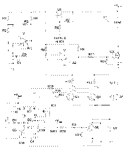
[0050] It is noted that a capacitor C4 is provided between the power source
and ground.
Capacitor C4 serves as a noise filter and to add stability to the circuit.
[0051] In an exemplary implementation of the embodiment of Figure 4, with load
Ll being
a lamp, the resistors and capacitors shown may have the following values:
Rl: 56 kC
R2: 56 kQ
R3: 56 kQ
R4: 2.2 kcI
R5: 56 kg
R9: 1 kS2
R10: 1 kS2
R18: 56 kS2
R20: 2.2 kS2
R22: 56 kS2
R23: 10 kS2
R24: 15 kS2
R25: 151c
R26: 10 kL
R27: 2.2 kg
-17-
CA 02483261 2004-10-25
WO 03/096135 PCT/US03/13106
R28: 2.2 kg
Cl: 0.1 F
C2: 1 F
C3: 0.1 F
C4: 100 F
C5: 100 pF
[0052] Figures 5A and 5B depict a fourth embodiment of the invention. The
circuit shown
in Figure 5A is similar to, and operates similarly to, the circuit shown in
Figure 4; therefore,
a detailed description of Figure 5A will be omitted. In particular, Figure 5A
differs from
Figure 4 only in the following aspects: (1) the addition of resistors Rl 1,
R29, and R38; (2)
the addition of capacitor C6; and (3) a change in the location of diode D6.
Figure 5A also
explicitly depicts a battery B 1 as the power source supplying Vbatt and
includes labeled
nodes A and B, which labels are used in connection with Figure 5B.
[0053] The changes between the third and fourth embodiments, as discussed
above, exist in
part to accommodate a charging circuit. The charging circuit is shown in
Figure 5B and is
connected to nodes A and B in Figure 5A, as indicated. A voltage source is
provided at re-
charge connector RC. Examples of such a voltage source include an AC adapter
and a car
cigarette lighter plug. Resistors R30 and R31, which may, alternatively, be
implemented in
the form of a single resistor having desired characteristics (e.g., in an
exemplary
implementation, R30 and R31 are 56 S2, 3W resistors, giving a total of 28 S2,
6W for the
combination), are used to limit voltage and current (in the exemplary
implementation, the
resulting available current is approximately 300 mA). The resulting current is
fed to the
emitter of transistor Q7, and the output is taken from the collector of Q7,
through diode D9,
to battery B 1 (in Figure 5A) to charge battery B 1. Diode D9 serves the
purpose of
preventing current from flowing back into the charger when no charging source
is
-18-
CA 02483261 2004-10-25
WO 03/096135 PCT/US03/13106
connected. Resistor R32 connects one terminal of the combination of R30 and
R31 with the
base of transistor Q7. Transistor Q7 is "turned on" through resistor R33 and
transistor Q8.
When transistor Q8 is "on," transistor Q7 allows charge to flow between its
emitter and
collector. Transistor Q8 is biased "on" via resistor R34 and is biased "off'
when transistor
Q9 is turned "on." Transistor Q9 is turned "on" and "off' by the combination
of variable
resistor VR1 and Zener diode D8. When a desired battery voltage is reached by
battery B 1,
Zener diode D8 becomes biased, and enough voltage becomes present at variable
resistor
VR1 to bias transistor Q9 "on." In turn, transistor Q8 is biased "off," and
the output current
of the charger reduces to a level required to hold the desired voltage at
battery B1. Resistor
R35. and capacitor C7 serve to provide stability and prevent oscillation. The
combination of
resistor R37 and diode D7 serves to prevent operation of the load L1 (see
Figure 5A) during
the charge process.
[00541 In an exemplary implementation of the embodiment of Figures 5A and 5B,
where
load LI is a lamp, the various resistors and capacitors take the following
values:
Rl: 56kn
R2: 56 kg
R3: 56 kQ
R4: 2.2 kQ
R5: 56 kSZ
R9: 1 1c
RIO: 1 kSZ
R10: 2201c-Q
R18: 56 kSZ
R20: 2.2 M
R22: 56 kc
-19-
CA 02483261 2004-10-25
WO 03/096135 PCT/US03/13106
R23: 56 kS2
R24: 100 kS2
R25: 100 kS2
R26: 10 kI
R27: 2.2 kS2
R28: 2.2 kS2
R29: 22 S2
R30: 56 SZ
R31: 56 S2
to R32: 4700
R33: 1 kS2
R34: 10 kS2
R35: 470 kS2
R36: 10M
R37: 4.71cS2
R38: 4.7 kS2
VR1: 101cSZ
Cl: 0.1 F
C2: 10 F
C3: 0.1 F
C4: 100 F
C5: 0.1 F
C6: 2200 pF
C7: 0.1 F
-20-
CA 02483261 2004-10-25
WO 03/096135 PCT/US03/13106
[0055] Figure 8 depicts a circuit diagram implementing a fifth embodiment of
the invention.
This embodiment is centered around an integrated circuit, IC8, which is
preferably a timer
circuit, for example, the 555 timer circuit shown in Figure 8. In this
embodiment, IC8
replaces the waveform generation amplifier circuits in the previous
embodiments and acts as
a controlled square-wave generator whose output controls current flow through
load L8
(which, in one embodiment, may be a lamp).
[0056] In particular, the timer circuit IC8 in Figure 8 is arranged as a free-
running oscillator
circuit, and its output is taken from Pin 3 through resistor R88 to the
transistor Q83, which
controls current flow through load L8. Transistor Q83 is shown in Figure 8 as
being a
bipolar transistor, but it may alternatively be implemented as a field-effect
transistor. The
output of the timer circuit IC8 is a square wave whose duty cycle is, in part,
determined by
the voltage at Pin 5, the control voltage input to timer circuit IC8. This
voltage is manually
controllable through the use of variable resistor VR8 (which would is coupled
to a knob,
slide, or the like, for user control).
[0057] Transistors Q81 and Q82, along with their surrounding resistors and
capacitors, are
arranged to form a low battery detection circuit. When the voltage of battery
B8 decays
below the threshold of Zener diode ZD8, transistor Q81 begins to turn off,
thus reducing the
voltage to the voltage divider network formed by resistor R82, variable
resistor VR8, and
resistor R817. This, in turn, reduces the control voltage input at Pin 5 of
timer circuit IC8,
resulting in a reduced duty cycle of the output square wave at Pin 3. As the
battery voltage
decays, the voltage at Pin 5 will approach zero, and therefore, the duty cycle
of the output
square wave will be zero. This effectively turns off the circuit, thus saving
the battery from
total decay. Transistor Q82 serves the purpose of "snapping off' transistor
Q81 more
abruptly, thus making the shut-off less linear.
-21-
CA 02483261 2004-10-25
WO 03/096135 PCT/US03/13106
[0058] The left-hand side of Figure 8 consists of a voltage-regulated battery
charging
circuit. This battery charging circuit comprises transistors Q84, Q85, and
Q86, as well as
the surrounding components. An input (charging) voltage is obtained from DC
plug P8.
The output voltage of this battery charging circuit is a function of the
voltage produced by
the voltage divider comprised of resistors R814 and R815, this voltage being
used to turn
transistor Q85 on and off. A constant trickle charge is obtained through
resistor R813 and
diode D81.
[0059] The low voltage detection circuits described above accomplish two
objects of the
invention. First, the load power is automatically reduced to a lower level as
the battery
discharges, thus increasing "run time." Secondly, the battery is prevented
from totally
discharging, which could prevent the battery from being fully recharged to its
rated value, in
the case of a rechargeable battery.
[0060] As discussed above, a lamp may be embodied using any of the above-
described
control circuit embodiments by using an appropriate lighting element as load
L1. Figure 6
depicts a further embodiment of such a lamp, including an additional cold-
cathode
fluorescent lamp (CCFL). As shown in Figure 6, in addition to lamp Ll, there
is a CCFL
L2. CCFL L2 is turned on and off using switch SW2, which, in a preferred
embodiment, is
a push-button-type switch, but which may comprise any other appropriate
switch.
[0061] Figure 7 depicts an embodiment of a circuit that supports the
embodiment shown in
Figure 6. As shown, battery B1 is connected to the (Ll) lamp circuit (i.e.,
one of the above-
described embodiments), but it is further connected to provide DC power
through switch
SW2. When switch SW2 is depressed (or otherwise actuated) so as to turn on the
CCFL,
DC power is provided to inverter Inl, which converts it to a relatively high-
frequency, high-
voltage, low-current AC signal. Lamp L2 is a CCFL. CCFLs are typically filled
with a gas
that activates to emit light at a voltage that lies between 180V and 800V.
Inverter Inl acts
-22-
CA 02483261 2004-10-25
WO 03/096135 PCT/US03/13106
to provide such a voltage at a low current level (in one implementation, the
current was
measured at 325 mA).
[0062] While Figure 7 shows switch SW2 interposed between battery B1 and
inverter Inl,
which is the preferred embodiment, switch SW2 could alternatively be
interposed between
inverter Inl and the CCFL L2.
[0063] The embodiments illustrated and discussed in this specification are
intended only to
teach those skilled in the art the best way known to the inventors to make and
use the
invention. Nothing in this specification should be considered as limiting the
scope of the
present invention. The above-described embodiments of the invention may be
modified or
varied, and elements added or omitted, without departing from the invention,
as appreciated
by those skilled in the art in light of the above teachings. It is therefore
to be understood
that, within the scope of the claims and their equivalents, the invention may
be practiced
otherwise than as specifically described.
-23-