Note: Descriptions are shown in the official language in which they were submitted.
CA 02483272 2004-10-21
WO 03/103048 PCT/US03/16136
DIE CONNECTED WITH INTEGRATED CIRCUIT COMPONENT
CROSS-REFERENCE TO RELATED APPLICATION
This application is a continuation-in-part of commonly-owned U.S. Patent
Application Serial No. (by Robert E. Stewart, filed May 24, 2002, and entitled
"COMPLIANT COMPONENT FOR SUPPORTING ELECTRICAL INTERFACE
COMPONENT"), which is hereby incorporated herein by reference in its entirety.
TECHNICAL FIELD
The invention in one example relates generally to electromechanical systems
and
more particularly to connection between parts in an electromechanical system.
BACKGROUND
A three dimensional die with multiple layers, as one example of an electrical
circuit,
requires electrical connections to multiple layers. For example, wire bonds
serve to provide
the electrical connections between the layers. In some cases, the wire bonds
must be made to
contacts on both the top and bottom of the die. Having wire bond contacts on
both the top
and bottom of the die can result in the need to fabricate subassemblies with
wire bonds
wrapping around multiple sides of the die. Having wire bonds that wrap around
multiple
sides of a die make the die difficult to package. Having wire bonds wrap
around the die
increases the periphery of the die. Having a larger periphery increases the
space used by the
die when the die is mounted to a substrate, circuit board, or the like. In
addition, wire bonds
are very thin and therefore susceptible to stress damage.
In another example, the die is packaged in a housing with electrical feed
throughs.
Wire bond contacts are made to electrical contacts on different layers of the
die. These bond
wires are then attached to feed throughs in the housing. The feed throughs in
the housing
CA 02483272 2004-10-21
WO 03/103048 PCT/US03/16136
allow for an interface with a substrate, circuit board, or the like. Creating
the wire bonds and
electrical feed through is complicated to assemble, expensive, and fragile.
In another example, the die has one or more layers. The die makes an
electrical
connection to a substrate, circuit board, or the like, of a different material
than the die. Since
the materials are different, they are likely to have different
expansion/contraction
coefficients. When expansion occurs in one or both of the materials, a stress
is placed on the
connection between the two materials. When the stress is large enough the
connection can
fail or break.
In another example, the die makes an electrical connection to a substrate,
circuit
board, or the like. When translational or rotational movement occurs a stress
is placed on the
connection between the die and the substrate, circuit board, or the like.
In another example, processing electronics are used in combination with the
die. Both
of the processing electronics and the die must make an electrical connection
to a substrate,
circuit board, or the like. Two separate connection spaces must be used on the
substrate,
circuit board, or the like.
In another example, the processing electronics and the die must go through
testing
together. To test the processing electronics and the die together they must be
installed to a
substrate, circuit board, or the like.
Thus, a need exists for a die that has increased durability in the interface
between the
die and a compatible structure. A need also exists for a die with decreased
size. A need also
exists for a die that is easier to electrically interface with compatible
structures. A need also
exists for a die and processing electronics to use a same connection space. A
need also exists
for a die and processing electronics to be tested before installation to a
substrate, circuit
board, or the like.
CA 02483272 2004-10-21
WO 03/103048 PCT/US03/16136
SUMMARY
The invention in one embodiment encompasses an apparatus. The apparatus
includes
a die with at least first and second portions, the first portion of the die
mechanically and
electrically connectable with a circuit board. The apparatus includes an
integrated circuit
component mechanically and electrically connected with the second portion of
the die. Upon
operation the die serves to generate one or more electrical signals that are
passed to the
integrated circuit component.
DESCRIPTION OF THE DRAWINGS
Features of exemplary implementations of the invention will become apparent
from
the description, the claims, and the accompanying drawing in which:
FIG. 1 is one example of an apparatus that includes a die that comprises one
or more
layers, one or more connection paths, one or more electrical contact
locations, one or more
electrical interface components, and one or more compliant components.
FIG. 2 is one exploded representation of the die of the apparatus of FIG. 1.
FIG. 3 is one example of an electrical connection between the die and a
separate layer
of the apparatus of FIG. 1.
FIG. 4 is a sectional representation of the die directed along line 4-4 of
FIG. 1.
FIG. 5 is a sectional representation of the die directed along line 5-5 of
FIG. 1.
FIG. 6 is a sectional representation of the die directed along line 6-6 of
FIG. 1.
FIG. 7 is one example of a compliant component of the apparatus of FIG. 1.
FIG. 8 is another example of the die of the apparatus of FIG. 1.
FIG. 9 is yet another example of the die of the apparatus of FIG. 1.
FIG. 10 is a further example of the die of the apparatus of FIG. 1.
CA 02483272 2004-10-21
WO 03/103048 PCT/US03/16136
FIG. 11 is one example of a wafer fabrication pattern of the die of the
apparatus of
FIG. 1.
FIG. 12 is a representation of the die of the apparatus of FIG. 1 and an
electrical
component receivable in a recess of the die.
FIG. 13 is a representation of the die of the apparatus of FIG. 1 and an
electrical
component connected with the die.
FIG. 14 is a representation of the die of the apparatus of FIG. 1 and an
electrical
component connected with the die.
FIG. 15 is a representation of one example of connection among the die, an
electrical
component, and a separate layer of the apparatus of FIG. 1.
FIG. 16 is a representation of one example of connection among the die and a
separate
layer of the apparatus of FIG. 1.
DETAILED DESCRIPTION
Turning to FIG. 1-3, an apparatus 100 in one example comprises one or more
dice
102 and one or more separate layers 310. The die 102 comprises, for example, a
micro-
electro-mechanical system ("MEMS"), sensor, actuator, accelerometer, switch,
stress
sensitive integrated circuit, or the like. The die 102 includes one or more
layers 160, 162,
164, one or more compliant components 104, 106, 108, 110, 112, 114, 116, 118,
one or more
electrical interface components 120, 122, 124, 126, 128, 130, 132, 134, and
one or more
connection paths 136, 138, 140, 142, 144, 146, 148, 120. The separate layer
310 in one
example comprises a substrate, circuit board, electronic device, die, or the
like.
Referring to FIGS. 4 and 5, the one or more layers 160, 162, 164 in one
example
comprises, semiconductors, insulators, conductors, or the like.
CA 02483272 2004-10-21
WO 03/103048 PCT/US03/16136
Referring to FIG. 6 (a cross section 6-6 of FIG. 1), in one example, the
compliant
component 116 is located in an etched well 610 on the cover 160 of the die
102. The well
610 is a large enough size and shape to allow for the flexing of the compliant
component 116.
In another example, the compliant component 116 is on a surface 180 of the
cover 160 of the
die 102.
Referring to FIGS. 1 and 7, the compliant component 114 in one example
comprises a
flexible arm 710. The flexible arm 710 is attached both to the die 102 and the
electrical
interface component 130. In one example, the die 102 is etched in a pattern
such that the arm
710 and the electrical interface component 130 have the space to be able to
flex in response
to stress applied to the flexible arm 710. In another example, the compliant
component 114 is
a beam that is micro machined into the die 102.
In one example, referring to FIG. 7, the compliant component 114 comprises a
flexible arm 710. In one example, the flexible arm 710 and the cover 160, or
the like, are
etched from a single homogeneous material. In another example, the flexible
arm 710 is
etched from a separate homogeneous material as the cover 160, then attached to
the cover
160, or the like. In another example, the flexible arm 710 is etched from a
heterogeneous
material as the cover 160, then attached to the cover 160, or the like.
In one example, the flexible arm 710 is a straight linear structure. In
another example,
the flexible arm 710 has one or more unstressed bends, or curves, or the like.
In another
example, the flexible arm 710 is a plurality of flexible arms.
Referring to FIG. 9, in one example a subset of the compliant components 108,
110,
116, 118 are designed to be compliant to translational movement in a single
direction as well
as being compliant with the direction of movement due to expansion. In one
example, the
translational movement in a single direction is horizontal on the die 102
plane. In another
example, the translational movement in a single direction is vertical on the
die 102 plane.
CA 02483272 2004-10-21
WO 03/103048 PCT/US03/16136
The compliant component 104, 106, 108, 110, 112, 114, 116, 118 orientation of
FIG. 9
allows the overall connection of the die 102 to the separate layer 310 to be
compliant to
translational movement in a single direction as well as being compliant with
the direction of
movement due to expansion.
Referring to FIG. 10, in one example first subset of the compliant components
108,
110, 116, 118 are designed to be compliant to translational movement in a
first direction as
well as being compliant with the direction of movement due to expansion. A
second subset
of the compliant components 104, 106, 112, 114 are designed to be compliant to
translational
movement in a second direction as well as being compliant with the direction
of movement
due to expansion. In one example the first direction is different from that of
the second
direction in the plane of the die 102. The compliant component 104, 106, 108,
110, 112, 114,
116, 118 orientation of FIG. 10 allows the overall connection of the die 102
to the separate
layer 310 to be compliant to translational movement in multiple directions,
.compliant to
rotation, as well as being compliant with the direction of movement due to
expansion. In one
example, the translational movement is horizontal on the die 102 plane. In
another example,
the translational movement is vertical on the die 102 plane. In another
example, the
translational movement is vertical and horizontal on the die 102 plane. A die
102 connection
compliant to translational, rotational, and expansion movements has a use in
applications that
are, in one example, counter balanced mechanical resonators. The resonators
have one or
more masses vibrating out of phase with each other. In one example, the masses
need to
vibrate at a same frequency. When used in such an application the compliant
mounting
structures 104, 106, 108, 110, 112, 114, 116, 118 that allow translational,
rotational, and
expansion movements will couple the two masses together so they vibrate at the
same
frequency.
CA 02483272 2004-10-21
WO 03/103048 PCT/US03/16136
The electrical interface component 130, in one example is a conductive pad, or
the
like. In another example, the electrical interface component 130 is a solder
ball, or the like.
In another example, the electrical interface component 130 is a solder ball,
or the like,
connected to a conductive pad, or the like. The electrical interface component
130 is
electrically insulated from the die 102.
In one example, the connection path 144 is a signal routing trace. The
connection
path 144 is used to pass the electrical signal from one of the one or more
layers 160, 162, 164
to the electrical interface component 130 on the interfacing surface 180.
In one example, a connection between the die 102 and the separated layer 310
can be
accomplished by using one or more of flip chip technology, ball grid array
technology and
pad grid array technology. Ball grid arrays are external connections that are
arranged as an
array of conducting pads on a interfacing surface 180 of the die 102. For
explanatory
purposes, the figures represent one example of the apparatus 100 that employs
exemplary ball
grid array technology. An electrical connection between a layer contact 190,
430, 432, 434,
436, 438, 440, and the electrical interface component 120, 122, 124, 126, 130,
132, 134 is
made through the connection path 136, 138, 140, 142, 144, 146, 148. In one
example, one or
more of the electrical interface components 128 are not used to electrically
interface the die
102 to the separate layer 310. In one example, the electrical interface
component 128 is extra
for the specific example of the die 102. In another example, the electrical
interface
component 128 is intended to accommodate a possible future increase in the
number of layer
contacts 190, 430, 432, 434, 436, 438, 440 in the die 102.
Referring to FIGS. l, 3, 4 and 5, in one example each of the layers 160, 162,
164, of a
die 102, requiring an electrical connection to a separate layer 310 brings its
connection to a
single interfacial surface 180 for interface with the separate layer 310. In
one example, to
CA 02483272 2004-10-21
WO 03/103048 PCT/US03/16136
access the various layers 160, 162, 164 of the die 102, one or more notches
150, 152, 154,
156 are created in the die 102.
In one example, the notch 156 could be a hole, cutout, path, window, opening
and/or
the like. The notch 156 can be at any location on the die 102. The notch 156
can be designed
to reach any or all levels and/or depths. One or more layer contacts 430, 432,
434, 436, 438,
440 can be reached through the same notch 156. Each of the notches 150, 152,
154, 156 can
be a different size, shape, or depth than any other of the notches 150, 152,
154, 156.
Referring to FIG. 11, the notch 156 is etched at the wafer level in order to
take
advantage of batch processing. In one example, the notches 150, 152, 154, 156
are etched on
the wafer to be a consistent size and depth. In one example, the notches 150,
152, 154, 156
are etched on the wafer to be different sizes and depths. In one example, the
etch could be an
anisotropic wet etch. In another example, the etch could be a dry reactive ion
etch, or the
like.
Referring to FIGS. 1-5, the layer contact 434 connection is brought to the
single
interfacial surface 180 by using a connection path 144. The connection path
144 uses the
notch 156 to reach the respective die 102 layer contact 434. An insulator 410
is used to
separate the connection path 144 from layer 160 and the other layer contacts
190, 430, 432,
436, 438, 440. In one example, the insulator 410 is a silicon dioxide
dielectric insulation
layer.
In one example, the die 102 has one or more layer contacts 430, 432, 434, 436,
438,
440 that are located on a different layer 162, 164 than the layer 160 being
used for interfacing
to a separate layer 310. Each layer 160, 162, 164 may have more than one layer
contact 190,
430, 432, 434, 436, 438, 440. An insulator 412, 416, 418, 420, 422, 426 is
used to separate
each layer 160, 162, 164 from the layer contacts 190, 430, 432, 434, 436, 438,
440 of the
CA 02483272 2004-10-21
WO 03/103048 PCT/US03/16136
other layers 160, 162, 164, and the other layers 160, 162, 164 themselves. In
one example,
the insulator 412, 416, 418, 420, 422, 426 is a silicon dioxide dielectric
insulation layer.
In one example, the die 102 and the separate layer 310 may not to be the same
material, and therefore may not have the same expansion coefficients. When the
die 102 and
the separate layer 310 are connected together and thermal changes, or any
other
expansionlcontraction force, occur the die 102 will expand/contract by one
amount and the
separate layer 310 expandslcontracts by another amount, different from that of
the amount of
the die 102. When the amount of expansion/contraction is different in the die
102 than in the
separate layer 310, there will be a stress applied at the connection of the
die 102 and the
separate layer 310. This stress is relieved at the connection between the die
102 and the
separate layer 310 by the flexing of the compliant component 114.
In one example, as shown in FIG. 1, 7, and 8, the stress applied to the
connection is
likely to be in a radial direction from/to the midpoint 158 of the die 102
tolfrom the electrical
interface component 130. In one example, the flexible arm 710 attached to the
electrical
interface component 130, is oriented perpendicular to the radial axis. When
the stress in
likely to be in a radial direction this perpendicular flexible arm 710
orientation provides a
unstressed starting point for the electrical interface component 130. This
unstressed starting
point provides wide range of motion in either radial direction. In another
example, as shown
in FIG. 8, the flexible arm 710 attached to the electrical interface component
130, is oriented
parallel to one or more of the die 102 edges.
Referring to FIGS. 4 and 5, in one example, the die 102 is a sensor system.
The die
102 has three element layers, a top cover 160, bottom cover 164, and a sensing
center
element 162. Each element layer 160, 162, 164 has a dielectric insulating
layer 412, 416,
418, 420, 422, 426 added to each surface that will be bonded to another
surface. A
conducting material 414, 424 is laid down on the dielectric insulating layer
412, 416, 418,
CA 02483272 2004-10-21
WO 03/103048 PCT/US03/16136
420, 422, 426 of each of the top cover 160, and the bottom cover 164 on the
surface that is
adjacent to the center element 162. A dielectric insulating layer 412, 416,
418, 420, 422, 426
is laid down over the conducting materials 414, 424. The three element layers
160, 162, 164
are bonded together.
In one example, a plurality of layer contacts 430, 432, 434, 436, 438, 440 are
buried
between the layers 160, 162, 164 of the die 102. The layer contacts 430, 432,
434, 436, 438,
440 are required to be on a interfacing surface 180 for the die 102 to be
mounted directly to
the separate layer 310, such as a substrate or circuit board. The interfacing
surface 180 has a
plurality of electrical interfacing components 120, 122, 124, 126, 128, 130,
132, 134.
Notches 150, 152, 154, 156 are made through the die 102 to expose the buried
layer contacts
430, 432, 434, 436, 438, 440. Along the walls of the notch 156 a dielectric
insulating layer
410 is applied to separate the connection path 144 from the element layers
160, 162, 164 and
the other layer contacts 430, 432, 436, 438, 440. The desired layer contact
434 will not be
covered by the dielectric insulating layer 410 to allow connection between the
layer contact
434 and the connection path 144. The connection path 144 is used to pass the
electrical
signal from the layer contact 434 to the electrical interface component 130 on
the interfacing
surface 180. In one example, the connection path 144 is a signal routing
trace. The electrical
interface component 130 on the interfacing surface 180 is attached to
compliant component
114. The compliant component 114 allows the die 102 to directly connect to the
separate
layer 310 with the same expansion properties or the separate layer 310 with
different
expansion properties.
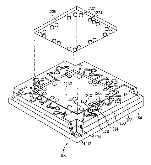
Turning to FIG. 12-15 an apparatus 100, in another example, comprises one or
more
dice 102, one or more electrical components 1220, and one or more separate
layers 310. The
die 102 in one example further comprises, one or more connection paths 1204
and 1206, and
one or more electrical interface components 1208 and 1210. The electrical
component 1220
CA 02483272 2004-10-21
WO 03/103048 PCT/US03/16136
in one example comprises one or more of processing electronics, central
processing unit
("CPU"), integrated circuit, and application specific integrated circuit
("ASIC"). The
electrical component 1220 in one example comprises one or more electrical
interface
components 1222 and 1224.
In .one example, the connection paths 1204 and 1206 are signal routing traces.
In one
example, the connection paths 1204 and 1206 comprise a conducting material.
The
connection path 1204 is used to pass the electrical signal from one of the one
or more layers
160, 162, 164, exposed by notch 156, to the electrical interface component
1208.
The one or more electrical interface components 1208 and 1210 in one example
comprise one or more of electrical contacts, conductive pads, and solder
balls. The one or
more electrical interface components 1208 and 1210 are electrically insulated
from the die
102.
Referring to FIG. 12, in one example, the electrical component 1220 and the
die 102
are made from a same material, and therefore are not likely to experience
differences in
expansion. In one example, the connection between the electrical component
1220 and the
die 102 can be accomplished by using one or more of flip chip technology, ball
grid array
technology, and pad grid array technology. In one example, the connection
between the
electrical component 1220 and the die 102 is made through one or more solder
balls. The one
or more solder balls electrically and mechanically connect the electrical
component 1220 to
the die 102. The one or more solder balls comprise a conductive material to
electrically
connect the electrical component 1220 to the die 102. The one or more solder
balls comprise
a bonding material to mechanically connect the electrical component 1220 to
the die 102.
In another example, the electrical component 1220 and the die 102 are made
from
different materials, and therefore are likely to experience differences in
expansion. In one
example, the expansion is due to one or more of thermal changes, material
aging, difference
CA 02483272 2004-10-21
WO 03/103048 PCT/US03/16136
in stability, and moisture swelling. In~ addition to one or more of flip chip
technology, ball
grid array technology, and pad grid array technology, the connection between
the electrical
component 1220 and the die 102, would benefit from using a compliant mounting
component
to support the electrical interface components 1208 and 1210. The compliant
mounting
component in one example comprises a structure similar to compliant component
114. The
connection between the electrical component 1220 and the die 102 using the
compliant
component 114 is forgiving to differences in relative movement between the
electrical
component 1220 and the die 102.
Referring to FIG. 12, an electrical connection, to route the electrical signal
between a
layer contact 1212 and the electrical interface component 1208, is made
through the
connection path 1204. The electrical interface component 1208 transfers the
electrical signal
to electrical interface component 1222 of the electrical component 1220. In
one example, the
electrical interface component 1222 comprises an input to the electrical
component 1220. In
one example, the electrical component 1220 processes one or more electrical
signals from the
die 102. In one example, the processed electrical signal results are placed on
electrical
interface component 1224 of the electrical component 1220. In one example, the
electrical
interface component 1224 comprises an output of the electrical component 1220.
The
processed electrical signal results are transferred to the electrical
interface component 1210
on the die 102. The processed electrical signal results are transferred to the
electrical
interface component 130 through the connection path 1206. The electrical
interface
component 130 is mounted to the flexible support, compliant component 114. In
one
example, electrical interface component 130 comprises a connection component
for
connection with the separate layer 310.
Referring to FIG. 15 in one example the die 102 and electrical component 1220
mount to a separate layer 310. The die 102 comprises one or more electrical
interface
CA 02483272 2004-10-21
WO 03/103048 PCT/US03/16136
components 1510, 1512, 1514, 1516, 1518, 1520, 1522, 1524, 1526, 1528, 1530,
1532, 1534,
1536, 1538, and 1540 to make connection to the respective electrical interface
components
1550, 1552, 1554, 1556, 1558, 1560, 1562, 1564, 1566, 1568, 1570, 1572, 1574,
1576, 1578,
and 1580 of the separate layer 310. In one example, the electrical interface
component 1550
comprises an input of the electrical component 1220. In another example, the
electrical
interface component 1550 comprises an output of the electrical component 1220.
In one
example, the electrical interface component 1550 is connected to the
electrical interface
component 1592 through a connection path 1590. The electrical interface
component 1592
comprises one or more connections slots 1594 to electrically and physically
attach to a
separate component. The connection path 1590 in one example comprises a
conducting path.
Referring to FIG. 12-15, in one example, the electrical component 1220 is a
separate
chip. To integrate the electrical component 1220 to the die 102, an electrical
and mechanical
connection is made between the electrical interface components 1208 of the die
102 and the
electrical interface components 1222 of the electrical component 1220. In one
example, the
electrical component 1220 electrically connects at the interfacing surface
180. In another
example, the electrical component 1220 electrically connects in a recess 1250
of the die 102.
The recess 1250 is designed so that the electrical component 1220 can rest in
the recess 1250.
The depth of the recess 1250 is designed so that when the die 102 and the
electrical
component 1220 are connected to the separate layer 310 the electrical
component 1220 is not
obstructing the electrical interface component 1510 of the die 102 from making
contact with
the electrical interface component 1550 of the separate layer 310.
Referring to FIG. 14, in one example, the electrical components 1220 are
completely
integrated into the die 102 by designing the die 102 to include the electrical
components
1220. The one or more of the electrical signals generated by the die 102 are
fed directly to
the integrated electrical components 1220.
CA 02483272 2004-10-21
WO 03/103048 PCT/US03/16136
Referring to FIG. 12-15, having the electrical component 1220 within the
periphery
the die 102 creates a higher level of integration. Rather than having the
electrical component
1220 and the die 102 use separate footprints, integrating them uses a single
footprint on the
separate layer 310. Thus, saving space on the separate layer 310.
Having the electrical component 1220 integrated into the die 102 allows for
testing of
the electrical component 1220 and the die 102 together without complete
installation to the
separate layer 310.
Turning to FIG. 16, in one example, the attachment of the die 102 to the
separate
layer 310 is made with one or more of electrical interface components 1512.
Electrical
interface component 1512 of the separate layer 310 is connected to the die 102
through the
electrical interface component 1552. In one example, the connection between
the die 102 and
the separate layer 310 is made through one or more solder balls. In one
example, the solder
ball is heated, centered, and cooled to complete the connection between
layers. In one
example, the solder ball is pressed together during the connection process,
thus the solder ball
is deformed from a spherical shape. The one or more solder balls electrically
and
mechanically connect the die 102 to the separate layer 310. The one or more
solder balls
comprise a conductive material to electrically connect the die 102 to the
separate layer 310.
The one or more solder balls comprise a bonding material to mechanically
connect the die
102 to the separate layer 310.
One or more features described herein with respect to one or more of the
compliant
components 104, 106, 108, 110, 112, 114, 116, 118 in one example apply
analogously to one
or more other of the compliant components 104, 106, 108, 110, 112, 114, 116,
118. One or
more features described herein with respect to one or more of the electrical
interface
components 120, 122, 124, 126, 128, 130, 132, 134 in one example apply
analogously to one
or more other of the electrical interface components 120, 122, 124, 126, 128,
130, 132, 134.
CA 02483272 2004-10-21
WO 03/103048 PCT/US03/16136
One or more features described herein with respect to one or more of the
connection paths
136, 138, 140, 142, 144, 146, 148 in one example apply analogously to one or
more other of
the connection paths 136, 138, 140, 142, 144, 146, 148. One or more features
described
herein with respect to one or more of the notches 150, 152, 154, 156 in one
example apply
analogously to one or more other of the notches 150, 152, 154, 156. One or
more features
described herein with respect to one or more of the electrical interface
components 130, 1510,
1512, 1514, 1516, 1518, 1520, 1522, 1524, 1526, 1528, 1530, 1532, 1534, 1536,
1538, and
1540 in one example apply analogously to one or more other of the electrical
interface
components 130, 1510, 1512, 1514, 1516, 1518, 1520, 1522, 1524, 1526, 1528,
1530, 1532,
1534, 1536, 1538, and 1540. One or more features described herein with respect
to one or
more of the electrical interface components 1550, 1552, 1554, 1556, 1558,
1560, 1562, 1564,
1566, 1568, 1570, 1572, 1574, 1576, 1578, and 1580 in one example apply
analogously to
one or more other of the electrical interface components 1550, 1552, 1554,
1556, 1558, 1560,
1562, 1564, 1566, 1568, 1570, 1572, 1574, 1576, 1578, and 1580.
~ The steps or operations described herein are just exemplary. There may be
many
variations to these steps or operations without departing from the sprit of
the invention. For
instance, the steps may be performed in a differing order, or steps may be
added, deleted, or
modified.
Although exemplary implementations of the invention have been depicted and
described in detail herein, it will be apparent to those skilled in the
relevant art that various
modifications, additions, substitutions, and the like can be make without
departing from the
sprit of the invention and these are therefore considered to be within the
scope of the
invention as defined in the following claims.