Note: Descriptions are shown in the official language in which they were submitted.
CA 02483645 2008-02-22
LIGHT- RECENING OR LIGHT- EMIT'TING DEVICE AND ITS PRODUCTION
IvIETHQD
R'RCHNICAL FIELD
The present invention relates to a light receiving or light emitting devioe
which can be deformed and eixnply manufactured by electricaUy connecting
particulate light receiving or light emitting semiconductor elements by means
of
linear condnctive members, and then sealing these elements with synthetic
resin,
and a method for manufacturing the same.
BACKGROUND OF THE INVENTION
Conventional solar cells are constructed with a flat=plate-form structure
overall, in which an n type diffusion la.yer is formed in the surface of a p
type
semiconductor substrate, a herring-bone-type light receiving surface electrode
is
formed near the front surface, and a back surface electrode is formed near the
back
swrfgce. In the case of such flat=plate-form solar cells, when the angle of
incidence
of sunlight on the solar cell becomes large in the morning or evening, the
reflectivity
at the surface increasee, so that the proportion of the sunlight that enters
the
interior of the solar cell drops.
In the past, therefore, various types of solar cell panels using eolar cells
oomprising spherical semiconductor eells with a diameter of approximately 1 to
2
mm have been proposed. For example, the inventor of the present application
has
proposed a solar cell and light emitting device compriaing a spherical
semiconduator
element as indicated in WO 98/15983. In such devioes, a diffusion Iayer, a pn
junction and a pair of electrodes positioned on both ends with the center of
the single
CA 02483645 2007-06-29
crystal silicon interposed are formed on a spherical p type or n type single
crystal of
silicon_ Numerous solar cells of the abovementioned type are disposed in the
form
of a matrix that has numerous rows and numerous columns; these cells are
connected in series and parallel, and are sealed in embedded form by a
transparent
synthetic resin, thus producing a solar cell panel. This solar cell is
advantageous in
that a plurality of solar cells of this type can be connected in series, since
a pair of
electrodes are formed on both ends of the solar cell. However, it is not easy
to
arrange a plurality of the solar cells in the form of a matrix, and to connect
these
numerous solar cells in a series=parallel connection.
For example, the inventor of the present application attempted to dispose a
plurality of solar cells in the form of a matrix in a sandwich configuration
between
two printed boards.
In this case, however, a plurality of solar cells must be precisely positioned
0.
on one printed board, and numerous electrodes must be connected; fiucthermore,
another printed board must be superimposed on this assembly, and numerous
electrodes must be connected here as well. Accordingly, the structure of the
solar
ceII panel becomes complicated, the size of the panel is increased, and the
cost of
parts and cost of aesembly are increased, so that the manufacturing cost of
the solar
cell panel is increased.
Here, panels with various types of structures have been proposed as solar
cell panels in which numerous spherical solar ceIls are disposed in the form
of a
matrix,
A solar cell panel in which numerous solar cells are connected in parallel via
two sheets of aluminum foil is proposed in Japanese patent laid-open
publication No.
6-13633.
-2-
CA 02483645 2007-06-29
In the solar cell panel or solar cell sheet described ia Japanese patent
laid-open publication No. 9-162434, a mesh is constructed from insulating warp
filaments and first and second woof filaments on which different metal coating
films
are formed; furthermore, numerous spherical elements in wbich a diffusion
layer is
formed on the surface of a p type spherical single cryetal of silicon are
manufactured,
these spherical elements are disposed in the respective eyes of the
abovementioned
mesh, the first woof filaments are connected to the diffusion layers, the
second woof
filaments are connected to the spherical single crystal of silicon, and these
elements
are sealed with synthetic resin.
In the case of this solar cell panel, the manufacture of the mesh having a
special structure is not easy, and the manufacturing cost i$ also high.
Furthermore,
since the spherical elements do not have electrodes, the first woof filament$
must be
coated with a substance that does not form an alloy with the p type spherical
elements, and the second woof filaments must be coated with a substance that
forms
an alloy with the p type spherical elements so that non-rectified contact is
possible.
Acmrdi.ng]y, there are restrictions on the substances that are respectively
used to
coat the first and second woof filamente, so that it is difficult to lower the
manufacturing cost. The second woof filaments and the p type spherical
elements
are heated at the time of alloy formation; however, since there is a danger
that the
donor of the n type diffusion layer formed in the surface will be diffused by
heating,
there are also restrictions on the substances that can be used as a donor, and
control
of the heating temperature is also difficult. In the photo power generating
panel described in Japanese patent laid=open
publication No. 2001-210$34, numerous spherical elements are manufactured in
which a diffusion layer is formed in the surface of a p type or n type
spherical
=3-
CA 02483645 2007-06-29
crystalline silicon, these spherical elements are inserted into numerous holes
formed
in a printed board, printed wiring is connected to the diffusion layers of the
numerous spherical elements, the diffusion layers of the numerous spherical
elements on the side of the back surface of the printed board are subsequently
b removed by etching, the printed board on which the numerous spherical
elements
have been incorporated is placed on top of another printed board, and the
spherical
crystals of the respective spherical elements are connected to the printed
wiring,
However, in the case of such a photo power generating panel, ginee the
numerous
spherical power generating elements are connected in parallel, the
electromotive
force of a aingle photo power generating panel cannot be increased, and since
two
printed boards are used, the cost of parts and cost of assembly are high, so
that the
manufacturing cost of the photo power generating panel is also increased.
Since
two printed boards are used, the panel tends to have a high riga.dity, so that
it is
difficult to construct a photo power generating panel with flexibility. In all
of the
abovementioned panels, the gap between the electrodes is reduced as the
spherical
diaraeter is reduced, so that it is difficult to reduce the size of the panel.
Furthermore, since the spherical light emitting elements do not have
independent
electrodes, individual testing for defective parts prior to the connection of
the
elements to the printed wiring is impossible.
Objects of the present invention are, to provide a light receiving or light
emitting device in which numerous particulate semiconductor elements each of
which has a pair of independent electrodes formed like a spot on both end
parts are
connected by means of conductive wire members, to provide a Iight receiving or
light
emitting device with flexibility, to provide a light receiving or light
emitting device in
which there are few restrictions on the material used as the conductive wire
member,
-4-
CA 02483645 2007-06-29
and to provide a light receiving or light emitting device in which numerous
particulate semiconductor elements can be connected by parallel connections or
series-parallel connections.
DISCLOSURE OF THE INVENTION
According to a fir$t aspect of the present invention, there is provided a
light
receiving or light emitting device comprising:
a plurality of paarticulate semiconductor elements disposed in at least one
column;
each semiconductor element of said plurality of elements having a
light-to-electricity transducing function or an electricity-to-light
transducing
function;
each eemiconductor element in said at least one column including opposing
end parts and a pair of opposing electrodes disposed on said opposing end
parts;
said pair of opposing electrodes interposing a center af each semiconductor
between said pair of opposing electrodes;
an axis between each pair of opposing electrodes being perpendicular to a
longitudinal axis of said at least one column;
eaid at least one column including flexible wires connecting in parallel each
semiconductor element disposed in said at least one column;
a space provided between adjacent semiconductor elements in said at least
one column so that said at least one column is capable of being flexed; and
a flexible covering material covering and embedding each semiconductor
element and each wire in said at least one column.
In light receiving or light emitting devices embodying this $,rst aspect of
the
-5-
CA 02483645 2007-06-29
invention, sinee a plurality of semiconductor elements that have electrodee
formed
in spot form on both end parts with the center interposed are lined up in at
least a
single row, and the semiconductor elements of the respective rows are
connected in
parallel by a pair of conductive wire members, the electrical connection of
numerous
semiconductor elements can be accomplished in a simple manner_ Since
semxconductor elements on which pairs of electrodes are formed are
incorporated,
there is no need for a complicated process of forming ohrni.c contacts between
the
semiconductor elements and the conductive wiring members; the electrodes of
the
semiconductor elements and the conductive wire members can easily be
electrically
connected by means of a low melting point metal such as solder or the like.
This light
receiving or light emitting device can be moulded in various shapes, and is
deformable as a result of the use of a soft covering material, so that the
device is
superior in terms of all-purpose utility.
If neeeasary, the various constructions set out below can also be applicable
in
16 embodiments of the first aspect of the present invention.
(a) A plurality of semiconductor elements are arranged in one row, and these
conductive wire members and covering material possess flexibility and are
constructed as a flexible cord.
(b) A plurality of semiconductor elements are arranged in a plurality of rows
on the
same plane, the conductive wire members and covering material possess
flexibility,
and the panel is constructed in the form of a panel with flexibility
(c) A plurality of semiconductor elements are arranged in a plurality of rows
on the
same plane, the covering material, is formed by a hard synthetic resin, and
the panel
is constructed in the form of a hard panel,
(d) The semiconductor elements in each row are connected in series to
-6-
CA 02483645 2007-06-29
semiconductor elements in the rows adjacent to tbis row by the conductive wire
members.
(e) Each of the semiconductor elements comprises a spherical element main body
made of a p type or n type semiconductor, and a pu junction, and the pair of
electrodes are connected to both ends of the pn junction.
(fl Each of semiconductor elements comprises a cylindrical element main body
made of a p type or n type semiconductor, and a pn junction, and the pair of
electrodes are connected to both ends of the pn junction.
(g) The semiconductor elements consist of light receiving elements, and the
panel
is a solar cell panel that receives sunlight and converts this light into
electricity_
(h) The semiconductor elements consist of light emitting elements, and the
panel is
a $urface =emitting light emitting panel.
(i) Partially cylindrical lens parts that correspond to the semiconductor
elements of
the respective rows are formed in the vicinity of the surface of the covering
material.
(j) A protective film is formed on at least one aurface of the covering
material.
(k) A reflective 51m that reflects light is formed on any one surface portion
of the
covering material.
According to a second aspect of the presnet invention, there is provided a
method for manufacturing a light receiving or light emitting device in which a
plurality of particulate semiconductor elements that have a light-to-
electricity
transducing function or an electricity-to-light transducing function are
incorporated
lined up in at least one column comprising'
a f=irst step in which a plurality of semiconductor elements, a temporary
faetening plate to which plural conductive wire members are temporarily
fastened
and a retaining plate having a plurality of retaining holes are prepared;
7
CA 02483645 2007-06-29
a second step in which $aid retaining plate is fitted into an opening part of
the temporary fastening plate, respective semiconductor elements are fitted in
the
retaining holes, and intermediate portions in the direction of height of the
semiconductor elements are held by the retaining holes; and
6 a third step in which the pairs of electrodes of said semiconductor elements
are electrically connected to the conductive wire members.
In embodiments of this method of the second aepect of the invention, since a
retaining plate comprising a plurality of retaining holes is inserted into the
opening
part of a temporary fastening plate to which conductive wire members are
temporarily fastened, a plurality of semicoAductor elements are fitted in the
plurality of retaining holes so that intermediate portions in the direction of
heigbt of
the semioonductor elements are holed, and the pairs of electrodes of the
semiconductor elements are electrically connected to the conductive wire
members, a
light receiving or light emitting device that possesses the various effects
and merits
described above can be manufactured easily and inexpensively.
In the third step of this method of the seeond aspect, the pairs of electrodes
of
the semiconductor elements may also be electrically connected to the
conductive wire
members by irradiating a metal film with a low melting point formed on the
surface
of the electrodes with a heating beam.
BRIEF DESCRIPTION OF THE DRAWINGS
Fig. 1 is a plan view of the temporary fastening plate and conductive wire
members in the present embodinaent,
Fig. 2 is a plan view of the retaining plate;
Fig. 3 is a sectional view of a solar cell;
s
;~;
CA 02483645 2007-06-29
Fig. 4 is a sectional view of another solar cell;
Fig. 5 is a sectional view of another solar cell;
Fig. 6 is a plan view showing the retaining plate engaged with the temporary
fastening plate, and solar cells inserted into the retaining holes;
Fig. 7 is an enlarged view of essential parts in Fig. 6;
Fig. 8 is a sectional view along VIII-VIII line in Fig. 6;
Fig. 9 is a perspective view of a cord-form solar cell;
Fig, 10 is sectional view of a cord-form solar cell;
Fig. 11 is a circuit diagram of the equivalent circuit of the solar cell shown
in
Fig. 9;
Fig. 12 is a perspective view of a solar cell in which cord-form solar cells
are
disposed in two rows;
Fig. 13 is a circuit diagram of the equivalent circuit of the solar cell shown
in,
Fig. 12;
Fig. 14 is a plan view of the temporary fastening plate, retaining plate and
conductive wire members in, another embodiment;
Fig. 15 is a plan view showing solar cells inserted into the retaining holes
..y.
shown in Fig. 14;
Fig. 16 is an enlarged view of essential parts in Fig. 15, showing a state in
which the retaining plate has been removed;
Fig. 17 is a sectional view along XVII-XVII line in Fig. 15 (in a state in
which
the retaining plate has been removed);
Fig. 18 is a sectional view along XVIII-XVIII line in Fig, 15 (in a tate in
which the retaining plate has been removed);
Fig. 19 is a sectional view showing a state in which the ao]ar cell is covered
9
CA 02483645 2007-06-29
by a covering material (in the state shown in Fig. 18);
Fig. 20 is a plan view of the covering material, solar cells and conductive
wire
members;
Fig. 21 is a plan view of the solar cell panel;
Fig. 22 is a circuit diagram of the equivalent circuit of the solar cell panel
shown in Fig. 21;
Fig. 23 is a sectional view of a modification of the solar cell panel;
Rg. 24 is a sectional view of another modification of the solar cell panel;
Fig. 25 is a sectional view of another modification of the solar cell panel;
Fig. 26 is perepective view of a cylindrical solar cell;
Fig. 27 is a circuit diagram of the equivalent circuit of the cylindrical
solar
cell shown in Fig. 26; and
Fig. 28 is a sectional view of a spherical light-emitting diode.
16 DETAILED DESCRIPTION OF PREFERRED EMBODIMENT OF THE
INVENTION
An embodiment of the present invention will be described below with
reference to the attached drawings.
The present embodiment is one example of a case in which the present
invention is applied to a cord-form solar cell used as a light receiving
device. First,
the method of manufacture and structure of this solar cell will be described.
First
of all, in a first step, as is shown in Fige, 1 through 5, a temporary
fastening plate 1
to which twelve conductive wire members 4 (positive pole wire members 4a and
negative pole wire members 4b) are fastened, a retaining plate 2, and (for
example)
120 semiconductor elements 3(hezeafter referred to as "solar cells"), are
prepared.
10-
;
CA 02483645 2007-06-29
The temporary fastening plate 1 is a rectangular plate with a thickness of
approximately 1 to 2 mm constructed from a hard synthetic resin (e. g., a
phenol type
or epoxy type synthetic resin) or the like.
A rectangular opening part 5 that is used to insert the retaining plate 2, and
a pair of projecting strips 6 in which twelve grooves used for the alternate
temporary
fastening of positive pole wire members 4a and negative pole wire members 4b
in
facing positions on the front and rear with the opening part 5 interposed are
formed,
are formed in this temporary fastening plate 1. The conductive wire members 4
possess flexibility and conductivity, and are (for example) metal wire members
(e. g.,
wire members made of copper, aluminum, silver, gold or the like) with a
diameter of
approximately 0.2 to 0.3 mm. The twelve wire members 4 are respectively
temporarily fastened in the grooves of the projecting strips 6, and are
arranged as
shown in the drawings, with both end parts being fastened by tapes 7 used for
temporary fastening. R.espective pairs of positive pole wire members 4a and
negative pole wire members 4b are disposed parallel to each other with a gap
that is
substantially equal to the diameter of the solar cells 3 being left between
the wire
members. The retaining plate 2 is a sheet-form plate with a thickness of
approximately 1 to 2 mm which is constructed from the same hard synthetic
resin as
the temporary fastening plate 1; this retaining plate 2 is fitted into the
opening
part 5 of the temporary fastening plate 1.
As is shown in Fig. 2, 120 hexagonal retaining holes 8 that are used for the
insertion of the solar cells 3 are formed in the retaining plate 2 in the form
of a
matrix with (for example) 20 rows and 6 columns. The retaining holes 8 of each
column are formed so that these holes are disposed betvveen the respective
pairs of
positive pole wire members 4a and negative pole wire members 4b. However, such
11
CA 02483645 2007-06-29
an arrangement of the retaining holes S in 20 rows and 6 columns is merely an
example; the present invention is not limited to 20 rows and 6 columns.
As is shown in Fig. 3, the particulate solar cells 3 each have a apherical
element main body 11 with a diameter of (e. g,) 1.0 to 1.5 mm consisting of p
type
single crystal silicon, an n type diffusion layer 12 (thickness: approximately
0.5 u
m) in which (for example) phosphorus (P) is diffused in the surface portion of
this
element main body 11, a substantially spherical eurfaoe form pn junction 13
that is formed in the boundary between the element main body 11 and diffusion
layer 12, a
flat part 14 formed in one end portion of the element main body 11, in which
no pu
junction is formed, a pair of electrodes 15, 16 (positive pole 15 and negative
pole 16)
that are disposed in spot form on both end parts with the center of the
element main
body 11 interposed, solder coating films that are formed on the surfaces of
the
respective electrodes 15, 16, and an SiOg coating film 17 (thickness:
approximately
0.4 g m) used for passivation which is formed on the surface of the diffusion
layer 12
except for the areas of the pair of electrodes 15, 16.
For example, this solar cell 3 can be manufactured by the method proposed
by the inventor of the present application in WO 98/15983. In this
manufacturing
method, a small piece of p type silicon is melted, and is allowed to drop
freely from
the upper end portion of a dropping tube. This silicon is solidified by
radiant
cooling when the silicon drops while being maintained in a spherical shape by
the
action of surface tension, so that a spherical single crystal silicon body is
created. A
diffusion layer 12, flat part 14, pair of electrodes 15, 16 and passivation
coating film
17 are formed in this spherical single crystal silicon body by well known
techniquee
such as etching, masking, diffusion treatments and the like.
The abovementioned pair of electrodes 15, 16 are respectively formed by (for
12-
CA 02483645 2007-06-29
i ,.
example) baking an aluminum paste or silver paste. The diameter of the
electrodes
15, 16 is approxcixnatel,y 300 to 500 u m, and the thickness is approximately
200 to
300 u m. However, the electrodes 15, 16 may also be formed by a plating
process,
or may be formed by some other method. Each solar cell 3 generates an
electromotive force with an open=circuit voltage of approximately 0.6 V when
the cell
receives sunlight with a light intensity of 100 mW/cm2. Here, in the solar
cells 3, p
type diffusion layers may be formed in n type silicon element main bodies, and
a pair
of electrodes and a passivation coating film may be formed in the same manner
as
described above. Alternatively, as is shown in Fig. 4, spherical solar cells
3A may be
lo used in which the flat part 14 of the solar cells 8 is not formed, and a
diffusion layer
12a, pn junction 13a, electrodes 15a, 16a, passivation film 17a are formed in
an
element main body 11a that is left in a spherical shape.
Furthermore, the particulate semiconductor elements need not always be
spherical; these elements may also be short cylindrical solar cells 3B as
shown in
Fig. 5. These solar cells 3B each comprise a short cylindrical element main
body
llb consisting of p type single crystal silicon (e. g., 1.0 to 1.5 mm 4), 1.0
to 1.6 mm
L), an n type diffusion layer 12b in the surface portion of this element main
body 11b,
a pn junction 13b, a p+ type diffusion layer 18 with a thi,ckmess of
approximately 0.2
u m formed by the diffusion of boron (B), a pair of electrodes 15b, 16b
(positive pole
15b and negative pole 16b) formed on both end parts in the axial direction of
the
element main body 1lb, a passivation coating film 17b consisting of Si02.
Next, in a second step, as is shown in Fig. 6, the retaining plate 2 is fitted
into the opening part 5 of the temporary fastening plate 1, and solar cells 3
are
respectively inserted into the 120 retaining holes 8 that are formed in the
retaining
26 plate 2. As i-s shown in Fig, 7, these solar cells 3 are placed in the
retaining holes 8
13
CA 02483645 2007-06-29
with the direction of conduction uniformly arranged, and intermediate portions
in 1 '
the, direction of height of the cells 3 are held by the retaining holes 8 so
that the
salder coating films of the positive poles 16 are caused to $dhere tightly to
the
positive pole wire members 4a, and the solder coating films of the negative
poles 16
are caused to adhere tightly to the negative pole wire members 4b. .9..s is
shown in
Fig. 8, the solar cells 3 are mounted in a state in which the temporary
fastening
plate 1 and retaining plate 2 are placed on a working bench 20 so that the
solar cells
do not fall out of the retaining holes 8.
Next, in a third step, as is shown in Figs. 7 and 8, the contact parts between
the positive pole wire members 4a and the solder coating iilms of the
electrodes 15
and the contact parts between the negative pole wire members 4b and the
sol.der
coating 5lma of the electrodes 16 are irradiated with a heating beam 21(la$er
beam
or infrared light beam), so that the positive pole wire members 4a and the
electrod.es
are electrically connected, and so that the negative pole wire members 4b and
the
15 electrodes 16 are electricaIly connected. In this way, the plurality of
solar cells 3 in
the respective columns are connected in parallel via the wire members 4a an
4b,
Next, in a fourth step, the retaining plate 2 is removed from the opening part
5 of the temporary fastening plate 1, and the wire members 4a and 4b and solar
ceIls
3 of the respective columns are coated from both the upper and lower sides by
placing a soft transparent synthetic resin (e. g., an EVA resin, siliCone
resin or the
like) in a semi-molten state.
Next, the solar cells 3 of the six columns are set in a specified metal mold
of a
molding apparatus together with the temporary fastening plate 1, and are
compression-molded by an appropriate pressing force, so that a covering
materia122
is formed which covers the wire members 4a and 4b and the 20 solar cells 3in
14- ;
CA 02483645 2007-06-29
embedded form as ehown in Figs. 9 and 10. Thus, when the 20 eolar cells 3 of
each
column covered by the covering material 22 are removed from the temporary
fastening plate 1, and the excess portions of the wire members 4a and 4b are
cut,
flexible cord-form solar cells 23 are completed with a cylindrical shape
having a
length of approximately 10 cm as shown in Fig. 9. If the solar ce]ls 8 in
these
cord-form solar cells 23 are indicated by diode symbols in the figures, then
the
equivalent circuit 24 of the solar cells 23 is as shown in Fig. 11. Here, the
20 solar
cells 3 are connected in parallel, the end parts of the positive pole wire
members 4a
constitute positive pole terminals 25a, and the end parts of the negative pole
wire
members 4b constitute negative pole terminals 25b.
Next, the functions and advantages of this cord=form solar cell 23 will be
described.
Since the respective solar cells S each generate an electromotive force with
an open-circuit voltage of approximately 0.6 V when the cells receive sunlight
with a
16 light intensity of 100 mW/cm2, the maximum electromotive force of the eord-
Eorm
solar cei123 is approximately 0.6 V. Since this cord-form cylindrical is
covered by a
transparent light-transmitting covering material 22, most of the light that is
incident inside the covering material 22 reaches the solar cells 3;
accordingly, the
light utilization rate is high, so that the power generating efficiency is
high.
A thin flexible light-weight solar cell that generates a photo-electromotive
force with a desired voltage and current can be constructed by lining up a
plurality of
these cord-form solar cells 23, and connecting these cells in a series
connection,
parallel connection or series-parallel connection_ Such a thin fleidble light-
weight
solar cell can be used as a power supply in various types of mobile electronic
devices
and the like.
CA 02483645 2007-06-29
In the manufacturing process of this solar cell 23, a plurality of solar cells
3 =
are respectively incorporated in the plurality of retaining holeg 8 of the
retaiuing
plate 2; moreover, intermediate portions in the direction of height of the
solar cells
$ are held, and the electrodes 15, 16 of the respective solar cells 3 are
connected to
th.e wire members 4a, 4b so that conduction is possible. Accordingly, the
disposition
and positioning of the numerous solar cells 3, and the electrical connection
of these
cells to the wire members 4a and 4b, can be accomplished easily and
effi.ciently.
Next, various examples in which the abovementioned embodiment is
partially modified will be described.
In addition to cylindrical shape, the shape of the cord-form solar cell 23 may
also be an angular column type shape, an oval cylindrical shape, or some other
cross-sectional shape. Furthermore, in cases where the cord-form solar cell 23
is
used "as is" in rod form, the covering material 22 may be formed as a
non=flexible
structure using a hard synthetic resin (e, g., a phenol type or epoxy type
synthetic
1 s resin or the like).
Alternatively, as is shown in Fig. 12, a plurality of cord-form solar cells 23
(e.
g., two c;ells) may be lined up in close proximity to each other, and
constructed as a
solar cell 23A in which the covering materials 22A are formed i-nto" an
integral unit.
In this solar cell 23, the solar cells 3 of the respective columns are
connected in
parallel by the wire members 4a and 4b, and two columns of solar cells 8 are
connected in series via the positive pole wire members 4a and negative pole
wire
members 4b, so that the photo-electromotive force is approximately 1-2 V as
shown
in the equivalent circuit in Fig. 13.
Next, a solar cell panel constituting another embodiment of the present 25
invention will be described with reference to Figs. 14 through 22, This
embodiment
-zs-
CA 02483645 2007-06-29
= ~, :
is one example of a case in which the present invention is applied to a planar
or
flat-plate-form solar ceil panel used as a light receiving device. The method
of
manufacture and structure of this solar cell panel will be described. Here,
parts that are the same as in the abovementioned embodiment are labeled with
the same
or similar numerals, and a description of such parts is omitted. Furthermore,
a
description is also omitted in the case of manufacturing steps that are the
same as
steps in the abovementioned embodiment.
First, in a first step, a temporary fastening plate XA, a retaining plate 2A
and
a plurality of solar cells 8(e. g., 1200 solar cells) are prepared in the same
manner as
in the abovementioned embodiment.
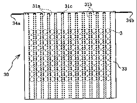
As is shown in Fig. 14, the temporary fastening plate 1A is similar to the
abovementioned temporary fastening plate 1> an opening part 5 and an a pair of
projecting strips 6 are formed in this temporary fastening plate 1A. Since
this
temporary fastening plate 1A is integrated with the covering material 33 (see
Fig.
19) that covers the solar cell pane130 in a subsequent step, this temporary
fastening
plate 1A is constructed from the same hard synthetic resin as the covering
material
33.
A plurality of positive pole wire members 31a and a plurality of negative pole
wire members 31b are provided as conductive wire members 31 that have
flexibility 20 and conductivity. As in the case of the abovementioned wire
members 4a and 4b,
these wire members 31 are temporarily fastened in the grooves of the pair of
projecting strips 6, and are arranged as shown in the figures.
The positive pole wire members 31a of each column and the positive pole
wire members 31b of the adjacent columns are connected by connecting parts
31c.
One end portion of each of the plurality of wire members 31a and 31b is
temporarily
sr?
17-
s
CA 02483645 2007-06-29
fastened by xneans of a temporary fastening tape 7. Positive terminals 34a
connected to the positive wire members 31a on the left side and negative
terminals
34b connected to the negative wire members 31b on the right side are
temporarily
fastened by means of the temporary fastening tape 7, respectively.
The retaining plate 2A is substantially similar to the abovementioned
retaining plate 2; however, 1200 hexagonal retaining holes 8 are formed in
this
retaining plate 2A in the form of a matrix with 10 rows and 12 columns. The
retaining holes 8 of each column are positioned between the respective
corresponding sets of wire members 31a and 31b. The solar ceUs 3 are the same
as
the solar cells of the abovementioned embodiment; accordingly, a description
of
these solar cells is omitted.
Next, in a second step, as is shown in Fig. 14, the retaining plate 2A is
fitted
into the opening part 5 of the temporary fastening plate lA; next, as is shown
in
Fig. 15, the solar eells 3 are placed in the respective retaining holes 8 of
the retaining
plate 2A in a state in which the direction of conduction is uniformly
arranged, so that
the electrodes 15 of the respective solar cells 8 are caused to adhere tightly
to the
wire members 31a, and so that the electrodes 16 are caused to adhere tightly
to the
wire members 31b.
Next, in a third step, the solder coating filnas of the electrodes 15 and 16
of
the solar cells 3 of each column are electrically connected to the positive
and
negative wire members 31a and 31b by irradiation with a heating beam in the
same
manner as in the abovementioned embodiment.
Next, in a fourth step, as is shown in Figs. 16 through 18, the retaining
plate
2A ia removed from the temporary fastening plate 1A. Next, as is shown in
Figs. 19
and 20, the upper and lower surfaces of the numerous solar cells 3 that are
18
, S.
CA 02483645 2007-06-29
positioned and held on the temporary fastening plate 1A via the wire members
31a
and 31b are coated vvith a semi-molten liquid of a transparent soft synthetic
resin (e.
g., an EVA resin, eiliwne resin or the like) to a thickness of approximately
500 to 700
u m. Then, these parts are set in a specified metal mold of a molding machine,
and
a covering material 33 that covers the wire members 31 and all of the solar
cells 3 in
embedded form is formed by compression molding using an appropriate pressing
force. In this case, the positive and negative terminals 34a, 34b are not
covered by
the covering material 33. Subsequentl.y, when cutting is performed in the
position
of the outer silhouette line of the covering material 33 without cutting the
positive
and negative terminals 34a and 34b, a thin plate-form or sheet-form solar cell
panel.
30 such as that shown in Fig. 21 is completed.
In order to heighten the light receiving performance with respect to aunlight,
partiaIIy cylindrical lens parts 35 (see Fig. 19) are formed on the surface of
the
covering materia133 so that these lens parts correspond to the respective
columns.
These lens parts 35 focus the incident sunlight, and cause this light to be
incident on the solar cells 3. However, in cases where this solar cell panel
30 is
incorporated in a specified location and used, the lens parts 35 may be formed
on one
side only. Moreover, hemispherical lens parts may be formed instead of
partiaIIy
cylindrical lens parts so that these lens parts correspond to the respective
solar celis
3- Since this solar cell panel 30 is constructed so that the panel receives
sunlight
that is incident from above and generates power, the upper surface of the
solar cell
panel 30 is the surface on the light receiving side, while the undersurface is
the
surfaee on the anti-light receiving side. In this solar cell panel 30, since
the
covering material 83 is formed from a soft synthetic resin, the panel has
ilexibility.
If the solar cells 3 of this solar ceA pane130 are indicated by diode symbols
in
-19-
CA 02483645 2007-06-29
the figures, then the equivalent circuit 36 of this solar cell panel 80 is as
shown in
Fig. 22. The solar cells 3 of each column are connected in parallel by the
wire
members 81a and 31b, and the solar ce]ls S of the respective columns are
connected
in series with the solar celle 3 of adjacent columns by the connecting parts
$1c.
Next, the functioRs and advantages of this solar ceJl panel 30 will be
described.
Each solar ce113 generates a photo-electromotive force of approximately 0.6
V when the cell receives sunlight; accordingly, the solar eells 3 of the
respective
columns also generate a photo-electromotive force of approximately 0.6 V. In
thie
solar cell panel 30, since 12 columns of solar cells 3 are connected in
series, the
maximum photo-electromotive force is approximately 7.2 V. Furthermore, in
cases
where a photo-electromotive force exceeding 7.2 V is required, such a
photo-electromotive force can be obtained by connecting a plurality of solar
cell
panels 30 in series via the respective terminals 34a and 34b. Furthermore, in
cases
where it is desired to increase the current of the photo-electromotive force,
this can
be accomplished by connecting a plurality of solar cell panels 30 in parallel,
and in
cases where it is desired to increase both the voltage and the current, this
can be
accomplished by connecting a plurality of solar cell panels 30 both in
parallel and
series.
This solar ceA panel 30 can be used in household solar power generating
~s'ystems, various types of solar power generating systems used in mobile
entities
such as automobiles, electric trains, boats and the like, solar power
generating
systems used as compact power supplies in electronic equipment or electrical
equipment, and other types of solar power generating systems such as chargers
or
the like_ Since the covering material is formed as a flexible structure using
a soft
CA 02483645 2007-06-29
synthetic resin, the solar cell panel 30 can be incorporated on curved
surfaces, and
can be disposed in the form of a cylinder. Accordingly, the solar cell panel
30 can
also be disposed and used in a state that conforms to the curved surfaces of
various
types of objects such as buildings, mobile entities or the like. For example,
the solar
6 cell panel can also be used in a state in which this panel is bonded to the
surface of
an automobile body or to the housing of a notebook computer. Furthermore,
since
the vrire members 31 are also flexible, the solar cell panel 30 can also be
molded into
a curved shape at the time of molding.
In this solar cell panel 30, solar cells 30 are disposed in the retaining
holes 8
formed in the retaining plate 2A, intermediate portions in the direction of
height of
the solar cells 30 are held in the retaining holes 8, and the electrodes 15
and 16 of
the respective solar cells 3 are joined with the wire members 31a and 31b by
means
of a heating beam. Accordingly, the disposition and positioning of the
numerous
solar cells 3 can be accomplished easily and efFiciently.
16 The numerous solar cells 3 are connected in series and parallel by means of
the wire'members 31a and 31b; accordingly, even in cases where solar cells 3
that
do not operate normally are present as a result of shade or some trouble, the
current
generated by normal solar cells 3 bypasses the solar cells 3 that are not
operating
normally, so that the drop in output can be minimized, and so that the ayetem
is
superior in terms of reliability. Furthermore, since a plurality of lens parts
35 are
formed on the solar cell panel 30, even if the angle of incidence of the
sunlight should
vary, reflection at the surface can be suppressed, and the sunlight can be
focused and
directed onto the solar ceUs 3; accordingly, the utilization rate of the
sunlight can
be increased.
However, in cases where the solar cell panel 30 is used in planar disposition,
-21=
CA 02483645 2007-06-29
the covering material 33 may also be constructed from a transparent hard
synthetic
resin material (e. g., an acrylic type resin, epoxy type resin, polyethylene
type resin,
polycarbonate or the like).
Next, examples in which the structure and method of manufacture of the
abovexnentioned solar cell pane130 are partially modified will be described.
1) As is shown in Fig. 23, a protective film 37 made of a hard synthetic
resin is formed on the surface of the solar cell panel 30A. The covering
materia133
can be protected by the protective film 37, so that durability can be ensured,
and a
drop in performance can be prevented. Furthermore, in cases where the solar
cell
z=
panel 80A is used in a fixed disposition, light that was not received by the
solar cells
3 can be reflected toward the solar cells 3 by installing a reflective film 38
or
reflective plate on the surface located on the opposite side from the surface
on which
sunlight is incident; accordingly, the efficiency of power generation can be
increased,
2) In the solar cell panel 30B shown in Fig. 24, both the upper surface and
undersurface are constructed as flat surfaces, and a protective film 37A made
of a
hard synthetic resin or a protective plate made of glass is disposed on both
the upper
eurfac8 and undersurface.
3) In the solar cell pane180C shown in Fig. 25, both the upper surface and
undersurface are constructed as flat surfaces; a protective film 37A made of a
hard
synthetic resin is disposed on the upper surface, and a reflective film 38A
made of a
metal film or metal plate is disposed on the undersurface. Since the upper
surface
on which the protective Mm 37A is formed is caused to face the side on which
the
sunlight is incident, the sunlight that passes through the solar ce]1 panel
30C is also
reflected by the reflective film 38A and reused; accordingly, the efficiency
of power
22
CA 02483645 2007-06-29
sA
generation is improved.
4) The aylindrical solar cell 40 shown in Fig. 26 is constructed from an
inner tube 41 that is made of a transparent or opaque synthetic resin or
metal, a
flexible solar cell panel 42 which is bent into a cylindrical shape and bonded
to the
6 surface of this inner tube 41, and an outer tube 48 used as a surface
protecting body
which is made of glass or a transparent syntheti.c resin, and which is fit
over the
abovementioned solar cell panel 42.
In this solar cell panel 42, as in the abovementioned solar cell panel 80,
solar
cells 3 are disposed in the form of a matrix with a plurality of rows and a
plurality of
columns_ A positive pole terminal 45a and negative pole terminal 45b are also
provided, as is shown in the equivalent circuit (see Fig. 27) of tkiis solar
cell panel 40.
Here, however, instead of the abowementioned inner tube 41, it would also be -
possible to use a semi-cylindrical body, partially cylindrical body, hollow
spherical
body, semi-hollow spherical body, partially hollow spherical body or eurved-
surface
body with a curved surface consisting of the same material as that described
above,
and to use a construction in which a light emitting panel is bonded to the
surface of
one of these bodies, and a surface protecting body made of glass or a
transparent
synthetic resin is bonded to the surface of this light emitting panel.
5) Various types of transparent synthetic resin materials (e, g., epoxy type
synthetic resins, acrylic type synthetic resins, silicone resins, polyethylene
type
synthetic resins, polycarbonates, polyimides, methacrylic resins and the like)
can be
used as the synthetic resin material that forms the covering material in the
abovementioned solar cell panel. Alternatively, both the abovementioned
temporary fastening plate lA and covering material 33 can be constructed from
a
#lexible synthetic resin, so that the solar cell panel is made easily
deformable.
.23-
CA 02483645 2007-06-29
6) In the abovementioned embodiments, solid solar cells 3 were described as an
example. However, hollow solar cells (not shown in the figures) that have a
light=to-electricity transducing function may also be ueed. Such hollow solar
cells
are cells in which the element main body 11 consisting of p type (or n type)
silicon is
6 hollow. In cases where such hollow element main bodies are manufactured, p
type
silicon melted in a quartz crucible is dropped as liquid droplets containing
gas
bubbles inside a dropping tube from the tip end of a quartz nozzle, and these
liquid
droplets are solidified into a sphexical shape while being dropped. In this
case,
liquid droplets containing gas bubbles can be formed by fillin$ the interiors
of the
liquid droplets of molten silicon witb a specified amount of an inert gas such
as
argon or the like immediately prior to the dropping of the molten p type
silicon
inside the dropping tube from the tip end of the quartz nozzle.
7) In regard to the solar cells 3 of the abovementioned solar cell panels, a
case in which silicon was used as the semiconductor was described as an
example;
16 however, p type or n type Ge can also be used as the semiconductor that
forms the
element main bodies of the solar celle 3, and various types of compound
semiconductors (e. g., GaAs, GaSb, InSb, InP, In,As or the like) can also be
used.
8) An inverter circuit that converts the direct-current power generated by
the solar cell panel into alternating-current power, and various types of
switches,
wirin.g and the like, can be incorporated in the extra space on the outer
circumferential side of the solar cell panel.
9) In the abovementioned embodiments, a solar cell panel used as a light
receiving panel, which used solar cells 3 as particulate semiconductor
elements, was
described as an example. However, particulate Iight-emitting diodes that have
an
26 electricity-to=light transducing function can be used instead of solar
cells 3. If a
-24-
CA 02483645 2007-06-29
construction is used in which such light-emitting diodes are connected in
series in a
plurality of stages, and a subetantially specified direct-current voltage is
applied to
the light-emitting diodes of the respective stages, a light-emitting panel or
display
that shows suxface light emission can be constructed.
The method used to manufacture such particulate light-emitting diodes
(spherical light-emitting diodes) is similar to the method proposed by the
inventor of
the present application in WO 98/15983; accordingly, the structure of these
spherical light-emitting diodes will be briefly described here.
As is shown in Fig. 28, a spherical light-emitting diode 50 comprises an
element main body 51 consisting of n type GaAs with a diameter of 1.0 to 1.5
mm, a
substantially spherical-surface form p type diffusion layer 52 that is formed
in the
vicinity of the surface of the element main body 51, a substantially spherical-
surface
form pn junction 53, an anode 54 and cathode 55, a fluorescent coating film 56
and
the like. The element main body 51 is constructed from n type GaAs to which Si
is
added so that the peak wavelength of the infrared light generated by the pn
junction
53 is 940 to 980 nm. The p type diffusion layer 52 is formed by thermally
diffusing
a p type impurity such as Zn; the impurity concentration at the surface of the
p
type diffusion layer is 2- 8 X 10¹⁹Icm3.
The fluorescent coating film 56 uses different fluorescent substances
according to the color of the light that is emitted.
Yo.74Ybo.z5Ero,oiOC1 is used as a fluorescent substance that generates red
light,
Yo.s4"Ybo.16Ero.o1Fs is used as a fluorescent substance that generates green
light, and
Yo.s6Ybo.s6Tmo.oo1F3 is used as a fluorescent substance that generates blue
light.
The abovementioned anode 54 (thickness 1 u m) is constructed from Au to which
1%
Zn is added, and the cathode 55 (thickness 1 m) is constructed from Au to
which
CA 02483645 2007-06-29
small amounts of Ge and Ni are added.
In such a particulate light-emitting diode 50, when a voltage of
approximately 1.4 V is applied to the cathode 56 from the anode 54, infrared
light
with a wavelength of approximately 940 to 980 nm is generated from the pn
junction
of the GaAs, and the fluorescent substance of the fluorescent coating film 56
is
excited by this infrared light so that the infrared light is converted into
visible light
(red light, green light or blue light) that corresponds to the fluorescent
substance,
and this visible light is output to the outside from the entire surface of the
fluorescent coating film.
For example, if all of the solar cells 3 of the abovementioned solar cell
panel
30 are caused to mount light-emitting diodes that emit red light, and a
direct-current voltage of approximately 1.4 V is applied to the cathode side
terminal from the anode side terminal, a light emitting panel is obtained in
which red light is
emitted by surface light emission from 1201ight-emitting diodes. A light
emitting
panel that generates green light and a light emitting panel that generates
blue light
can be similarly constructed.
Furthermore, a light emitting panel that can be used as a display for
displaying characters, symbols and images in a single color or a plurality of
colors
can also be constructed. A color display or color television in which light-
emitting
diodes for the abovementioned R, G and B (red, green and blue) are
incorporated can
also be constructed as proposed in the abovementioned WO 9$/159$3_ Here, the
types and combinations of light-emitting diodes that are incorporated in the
light
emitting panel, and the disposition configuration of the plurality of light-
emitting
diodee, are set in accordance wxth the size and function of the display or
television.
Furthermore, the diameter of the element main bodies 51 of the particulate
26
CA 02483645 2007-06-29
light-emitting diodes 50 is not limited to the value described above; this
diameter
may also be set at a value that is less than 1.0 mm, or a value that is
greater than
1.5 mm.
Furthermore, hollow element main bodies can also be used as the element
main bodies 51 of the abovementioned spherical light-emitting diodes 50;
alternatively, element main bodies in which insulating spherical bodies
consisting of
an insulating material are incorporated instead of hollow parts may also be
used.
Furthermore, not only planar panels, but also light emitting devices formed
in a cylindrical shape as shown in Fig. 26, can be formed, Furthermore,
instead of
the GaAs used as the semiconductor forming the abovementioned element main
bodies, GaP, GaN or various other types of semiconductors can be utilized as
the
semiconductor used in the abovementioned light-emitting diodes. Moreover, the
shape is not necessarily limited to spherical; this shape may also be
cylindrical or
the like.
.~r.'
, . t=
- 27 -