Note: Descriptions are shown in the official language in which they were submitted.
CA 02485040 2004-07-26
WO 03/065537 PCT/US03/02147
Dual Transformer High Frequency Battery Charger
BACKGROUND OF THE INVENTION
Field of the Invention
The present invention relates to a battery charger or
booster and in particular to a high frequency charger.
Technical Background
Dual-mode battery chargers currently exist. When
operated in a first mode, the battery charger delivers
a high current output for a short duration of time.
This short duration, high current can be used to jump-
start a vehicle with a dead battery. In a second mode,
the battery charger provides a low current output that
is used to charge the battery back to its full charge.
Known dual-mode battery chargers typically use a single
large transformer to achieve the dual-mode capability.
The single transformer is usually a linear type
transformer. A tap of a primary winding of the
transformer is changed in order to achieve the dual
capability with the linear-type transformer. As the
tap of the transformer is changed, the output voltage,
and hence, according to Ohm's Law, the output current
of the transformer is changed, resulting in the dual-
mode capability. Use of a single transformer for both
modes of operation has the advantage of being very
cost-efficient and very effective.
However, this approach also has several disadvantages.
One of the disadvantages is that single transformer
battery chargers are very large and cumbersome.
Standard linear transformers require iron for their
cores, adding to the weight of the battery charger.
They also require orders of magnitude more wire to form
1
CA 02485040 2004-07-26
WO 03/065537 PCT/US03/02147
their windings than do high frequency chargers, again
adding to the weight of the battery charger.
Additionally, although the linear transformer can
provide a high current output, the high current output
can only be provided for a very short period of time.
As the transformer operates in high current mode, it
generates an excessive amount of heat. In fact, so
much heat may be generated that the transformer
actually melts down. If a meltdown occurs, the
transformer will not operate in either the high current
mode or the low current mode. Linear transformers are
also very lossy in terms of magnetic losses and eddy
current losses, resulting in inefficiency.
Additionally, a characteristic of liquid electrolyte
type batteries, particularly lead acid batteries used
in vehicles, is that chemical compound deposits slowly
build up on the plates to partially or entirely cover
and displace the normal plate surfaces. Low current
recharging is inadequate in that it can not, as such,
sufficiently remove such deposits that with the passage
of time crystallize and choke the battery plates by
interfering with electrolyte movement. When this occurs
a battery may still appear to have taken a charge and
even the electrolyte may check as being correct, but
the battery does not hold the charge because the plates
are effectively shorted. Batteries using other
electrolytes also face reclaiming, maintenance and
charging problems that need to be successfully
addressed.
Thus, there is a need for a method to release the
deposits that are built up on the plate surfaces, where
the deposits may either go back into the solution or be
2
CA 02485040 2004-07-26
WO 03/065537 PCT/US03/02147
broken up. There is also a need for a simple and
lightweight dual-mode battery charger. The battery
charger should be able to provide a high current output
that is sufficient to start an automobile or other
vehicle with a dead battery, yet be easy to construct
and safe to operate.
SUMMARY OF THE INVENTION
According to an embodiment of the invention, there is
provided a high frequency charger that includes a
charge circuit and a boost circuit. In a preferred
embodiment, the charge circuit includes a first high
frequency transformer. A switch switches this first
high frequency transformer at a predetermined
frequency. The boost circuit includes a second high
frequency transformer that is separate from the first
high frequency transformer in the charge circuit. The
first and second high frequency transformers are
operated in a similar manner. However, the boost
circuit is adapted provide a high current that can be
used to jump-start a vehicle with a depleted battery.
In a preferred embodiment, a PV~IM controller provides a
driving signal to the switch such that the transformer
of the charge circuit is switched to output a pulse.
The pulse output of the charge circuit can be used to
condition the battery.
As noted, the transformer in the charge circuit and the
transformer in the boost circuit are preferably
separate from each other, that is, there are two
transformers and associated circuits. Thus, the
battery charger is not dependent on the same
transformer for both standard charging and boosting.
3
CA 02485040 2004-07-26
WO 03/065537 PCT/US03/02147
For example, if the transformer in a conventional
charger burns out while performing a boost function,
all the functionality of the charger may be lost, as
one transformer is used for both functions. However,
in the present embodiment, either of the transformers
still operates even if the other transformer is
disabled for some reason.
A control circuit for a high frequency charger is also
provided. In an exemplary embodiment, the control
circuit includes a pulse width modulation (PWM)
controller having a reference voltage input, a control
input, and an output for a control signal. A switch
receives the control signal and is switched on and off
in response to the control signal. A voltage divider
network divides the voltage applied to the reference
voltage input and the control input. A duty cycle of
the control signal output from the PWM controller
varies based on the percentage of the reference voltage
that is applied to the control.
In a further embodiment, the voltage divider network
comprises a first resistor having a first terminal
connected to the reference voltage input and a second
terminal connected to the control input. A plurality
of second resistors each has a first terminal connected
to the second terminal of the first resistor and a
second terminal. A plurality of transistors are also
provided, each having a first electrode connected to
the second terminal of one of the second resistors, a
second electrode that is grounded, and a third
electrode receiving an enable signal. The enable
signal turns the transistors on and off, selectively
connecting one of the second resistors to ground.
4
CA 02485040 2004-07-26
WO 03/065537 PCT/US03/02147
According to another aspect of the invention there is
provided a computer-readable storage medium for use
with a computer for controlling a high frequency
charger including a charge circuit having a first high
frequency transformer; a first switch switching the
first high frequency transformer at a predetermined
frequency for producing a charge signal in a first mode
of operation; the charge circuit operating in at least
one of a pulse mode and a charge mode; and a selector
for selecting one of the charge mode and the pulse
mode, the computer-readable information storage medium
storing computer-readable program code for causing the
computer to perform the steps of: detecting a selected
mode of operation for the charger; and when a pulse
mode is selected, a) generating a driving signal for
the first switch for a first period of time; b)
disabling the first switch for a second period of time;
and c) returning to step a).
The above and other features of the invention, along
with attendant benefits and advantages will become
apparent from the following detailed description when
considered with the accompanying drawings.
BRIEF DESCRIPTION OF THE FIGURES
Figure 1 is a block diagram showing a dual high
frequency charger according to an embodiment of the
present invention.
Figure 2 is a diagram of waveforms generated by control
circuits according to an embodiment of the present
invention.
Figure 3 is a circuit schematic in partial block
diagram form showing an embodiment of the pulse enable
5
CA 02485040 2004-07-26
WO 03/065537 PCT/US03/02147
circuit and the pulse width modulation controller shown
in Figure 1.
DETAILED DESCRIPTION OF THE INVENTION
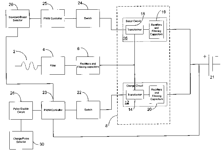
Referring now to Figure 1, there is shown a high
frequency charger, according one embodiment of the
invention, which includes a high frequency transformer
portion 8. The high frequency transformer portion 8
typically receives a DC signal as its input. The DC
signal can be provided from a battery or from an AC
input. In the embodiment illustrated, an AC input 2,
which may be provided by a typical wall-socket, is
coupled to a filter 4, for example, a pi filter or an
LC filter. The filter 4 is used to smooth and clean
the AC input. An AC signal output from the filter 4 is
provided to conventional rectifiers and filtering
capacitors 6 for rectifying the AC signal. The
rectifier is preferably a full-wave rectifier of a type
known to one skilled in the art and provides a DC
output of, for example, approximately 150 volts DC.
The full-wave rectified and filtered DC output from
rectifier 6 is provided to the high frequency
transformer portion 8 of the battery charger. The high
frequency transformer portion 8 includes a charge
circuit 12 and a boost circuit 16. The boost circuit
16 is used to provide a high current boost that can be
used to jump-start a vehicle with a dead battery. The
charge circuit 12 is used for normal charging of the
battery. The operation of the boost circuit 16 and the
charge circuit 12 may take place sequentially, in any
order, or simultaneously. The charge circuit 12 and the
boost circuit 16 each include a high frequency
6
CA 02485040 2004-07-26
WO 03/065537 PCT/US03/02147
transformer 14, 18, respectively. A DC output from the
rectifiers and filtering capacitors 6 is provided to
each of the high frequency transformers 14, 18.
Transformers typically receive an AC input and provide
S an AC output. For example, a transformer plugged into
an ordinary wall-socket is provided with a 120-Volt AC
input and outputs an AC signal that is dependent on the
secondary winding of the transformer. Thus, high
frequency transformers 14, 18 need to be manipulated to
behave so that the DC signal from rectifiers 6 looks
like an AC input. This manipulation is accomplished by
switching the DC output from rectifier 6 through the
high frequency transformers. The transformers are
turned on and off at a high frequency, for example,
about 20kHz and above. This switching causes the
transformers to~behave as though their input is AC.
This switching can be accomplished using essentially
any type of switch, for example, a field effect
transistor (FET) or other electronic switch. The high
frequency transformers 14, 18 of the illustrated
embodiment are switched by switches 22, 24,
respectively, coupled thereto. The switches 22, 24
are, in turn, controlled by P4VM controllers 23, 25.
The PWM controller may be, for example, a TL 494
Motorola type controller or a discrete controller. The
PWM controller generates a PWM driving signal for
turning the switches on and off.
The charge circuit 12 is capable of operation in two
modes, a charge mode and a pulse mode. In the charge
mode, the charge circuit 12 operates to charge a
battery. In the pulse mode, the charge circuit 12
operates to condition or desulfate a battery. A user
7
CA 02485040 2004-07-26
WO 03/065537 PCT/US03/02147
may select between one of these two modes via selector
30. The selector 30 provides the user's selection to a
pulse enable circuit 28. The pulse enable circuit 28
controls the PWM controller 23 in accordance with
whether the charge mode or the pulse mode of operation
is selected for the charge circuit 12.
When the pulse mode is selected, the pulse enable
v
circuit 28 controls the PWM controller 23 to
alternately be active and output a driving signal to
the switch 22 and be inactive and not drive the switch
22. A cycle of enabling/disabling the switching of the
switch 22 is repeated under the control of the PWM
controller 23. Figure 2 illustrates exemplary output
waveforms for the pulse enable circuit 28 and the PWM
controller 23. In the pulse mode, the pulse enable
circuit 28 is activated such that its output signal W1
varies between low and high states as shown in Figure
2. The PWM controller 23 is activated depending upon
the output signal W1 of the pulse enable circuit 28.
During a first time period tl, the output W1 of the
pulse enable circuit 28 is high and the PWM controller
23 is activated to generate a PWM driving signal W2, as
shown in Figure 2. The driving signal WZ of the PWM
controller 23 is provided to the switch 22, e.g., to
the gate of a FET comprising switch 22, to turn it on
and off. For example, the driving signal from the PWM
controller 23 may have a duty cycle of less than 15% so
that the FET is turned on for a very short period of
time, outputs current to the battery, and is then
disabled. The driving signal modulates the FET.
During a second time period t2, the output W1 of the
pulse enable circuit 28 is low and the PWM controller
8
CA 02485040 2004-07-26
WO 03/065537 PCT/US03/02147
is deactivated. No driving signal is provided to the
FET, and the FET remains off. Pulsing of the high
frequency transformer in this manner chops its output
to condition the battery.
During the pulse mode, a series of output current
pulses are generated by the battery charger and are
provided to the discharged battery 21. The current
pulses may have a frequency of about one pulse per
second and a rise time of about 100 volts/microsecond
or less .
The battery charger pulses the battery to perform the
conditioning. The switching of the FET switch 22 is
controlled to generate the conditioning pulses. For
example, the microprocessor may enable the PWM
controller 23 to switch the FET on and off for a period
of time, about 50 microseconds. The PWM controller 23
is then turned off, disabling the FET switch 22. The
FET is not switched when the PWM controller 23 is off.
The PWM controller 23 may remain off for about 1
second. The process then repeats until the battery
conditioning operation has been performed for 24 hours,
at which time the battery conditioning process is
completed.
When the charge mode is selected via selector 30, the
PWM controller 23 is preferably always activated.
Operation of the PWM controller 23 may be controlled in
part via feedback from the battery 21 being charged.
The duty cycle of the driving signal generated by PWM
controller 23 is varied based on the charging state of
the battery. A feedback signal from the battery being
charged 21 to the PWM controller 23 provides the
information on the charging state of the battery. The
9
CA 02485040 2004-07-26
WO 03/065537 PCT/US03/02147
more power the battery needs, the higher the duty
cycle; and the less power the battery needs, the lower
the duty cycle. Switch 22 switches transformer 14 in
accordance with the driving signal to charge the
battery 21.
Referring again to Figure 1, boost circuit 16 is now
described. Boost circuit 16 provides a high current
pulse that can be used to jump-start a vehicle with a
dead battery. The boost circuit 16 is enabled via a
standard/boost mode selector 26, which a user can
actuate. When actuated to select the boost mode,
selector 26 enables PWM controller 25 to generate a
signal that drives switch 24, which, in an exemplary
embodiment, comprises a FET. The frequency of the
driving signal for FET 24 in the high power boost
circuit 16 can be the same as or different from the
frequency of the driving signal for switch 22 in the
charge circuit 12, for example, about 20kHz, or even
higher. When the same frequency is used, the clock
frequency for the PWM controller 23 associated with the
charge circuit 12 to be shared by the PWM controller 25
for the high power boost circuit 16.
The high power boost circuit 16 receives a DC input
from the rectifier 6. The DC input is provided to high
frequency transformer 18 in the high power boost
circuit 16. Preferably, the high frequency transformer
18 in the high power boost circuit 16 is separate from
the high frequency transformer 14 in the charge circuit
12. The high frequency transformer 18 in the high power
boost circuit 16 outputs a relatively high current with
respect to the output of the charge circuit 12. For
example, the current output from the boost circuit 16
CA 02485040 2004-07-26
WO 03/065537 PCT/US03/02147
may range from about 30 amps to about 500 amps,
compared to about 2-25 amps for the charge circuit 12.
Additionally, the output from the boost circuit 16 is
typically only generated for a short period of time,
for example, about 3-40 seconds. Accordingly, the high
frequency transformer 18 in the high power boost
circuit 16 is preferably slightly larger than the high
frequency transformer 14 in the charge circuit 12.
The high frequency transformer 18 has a duty cycle such
that it may be on half the time and off the half the
time, even though there may always be an output from
the transformer that is rectified, filtered and used to
recharge the battery. The PWM controller 25 is
typically turned off for about 60-90% of the time and
is turned on for about 10-400, and then it is turned
back off again to achieve the duty cycle for the high
frequency charger. During the 10-40% of the time the
PWM controller 25 is on, switch 24 switches the high
frequency transformer. This provides a high current
pulse out of the high frequency transformer through
rectifier 19 to the battery to be charged.
Both the transformer 14 in the charge circuit 12 and
the transformer 18 in the boost circuit 16 output an AC
signal that needs to be converted to DC in order to be
used by the battery. Therefore, the output of the high
frequency charger in the charge circuit passes through
standard rectifiers and filtering capacitors 19, 20 to
provide a DC output. The high frequency transformer 14
in the charge circuit 12 is preferably a relatively
small transformer capable of delivering a relatively
low current, preferably between about between 2 and
about 30 amperes, and a voltage corresponding to
11
CA 02485040 2004-07-26
WO 03/065537 PCT/US03/02147
whatever the battery needs, for example, about 14.2
volts. The switching operation for the high frequency
transformer 18 in the high power boost circuit 16 by
switch 24 is preferably performed in a manner similar
S to that described above with regard to the charge
circuit 12 but, due to its different construction,
results in a current output from the boost circuit from
about 30 amps to about 500 amps.
Turning now to Figure 3, an example of circuitry that
may comprise the pulse enable circuit 28 is described.
In the illustrated embodiment, the pulse enable circuit
28 incorporates manual control of the PWM controller
23. A user can thus control the charging of the
battery. The PWM controller 23 has an input 31 to
which a reference voltage is applied, and a dead time
control input 32. The dead time control input 32
controls the duty cycle of the driving signal from
output 34 of the PWM controller 23 based on a
percentage of the reference voltage that is applied to
the dead time control input 32. For example, when the
full reference voltage is applied to the dead time
control input 32, the duty cycle of the output signal
of PWM controller 23 is set to zero, the switch 22
(Fig. 1) is off, and no voltage is applied to the
battery being charged. When no voltage is applied to
the dead time control input 32, the duty cycle of the
output signal of the PWM controller 23 is set to its
maximum, and a maximum current is applied to the
battery. The duty cycle of the driving signal from
output 34 of the PWM controller 23 varies between these
two extremes in dependence on the percentages of the
12
CA 02485040 2004-07-26
WO 03/065537 PCT/US03/02147
reference voltage applied to dead time control input
32.
In the embodiment shown in Figure 3, a combination of a
counter circuit 36 and a number of transistors 38-41 is
used to control the percentage of the reference voltage
that is applied to the dead time control input 32. The
counter 36 is preferably either a low active device
with diodes or a high output active decade counter, for
example a 4017B CMOS IC. Of course other arrangements
are possible within the scope of the invention.
Outputs of the counter 36 are each connected to
transistors. Four transistors 38-41 for four outputs
of counter 36 are shown in Figure 3. The number of
outputs and corresponding transistors may vary
depending upon the type of counter used. Each
transistor may be of a BJT or of a FET type. A control
electrode of each transistor 38-41 is connected through
a corresponding resistor 42-45 to a separate output of
the counter 36. A first electrode in the main current
path of each transistor 38-41 is coupled to ground. A
second electrode in the main current path of each
transistor 38-41 is coupled to a resistor 46-49,
respectively. Each of the resistors 46-49 is coupled
to the dead time control input 32 of the PWM controller
23. Each of the resistors 46-49 is also coupled to
resistor 51, which is, in turn coupled to the reference
voltage input 30 of the PWM controller 23.
The resistors 46-49, the associated transistors 38-41,
and the resistor 51 form a voltage divider. The voltage
difference between the reference voltage input 30 and
the dead time control input 32 is controlled by the
values of the resistors 46-49. For example, each of
13
CA 02485040 2004-07-26
WO 03/065537 PCT/US03/02147
the resistors 46-49 can be selected to have a different
resistance. The voltage drops across the resistors 46-
49 will vary accordingly. Thus, the percentage of the
reference voltage applied to the dead time control
S input 32 varies depending on which transistor 38-41 is
turned on and the value of its associated resistor 46-
49.
For example, as the counter 36 is clocked, one of the
outputs of the counter 36 becomes active and turns on
the respective transistor 38-41 connected to that
output. Only one of the transistors 38-41 may be
turned on at any one time. The turned on transistor
38-41 provides a current path from the dead time
control input 32, through its respective resistor 46-
49, to ground, thereby altering the voltage at the dead
time control input 32 with respect to the voltage at
the reference voltage input 30. Alternately, more than
one of the transistors 38-41 is turned on.
A switch 53, such as a push button switch, may be
coupled to a clock input 37 and used to clock the
counter 36. For example, actuating the switch once
clocks the counter 36 from the zero output to the first
output, actuating the switch a second time clocks the
counter 36 to the second output, and so on. As each
output of the counter 36 becomes active, the transistor
associated with that output turns on, altering the
voltage at the dead time control input 32. Thus, the
duty cycle of the driving signal from PWM controller 23
can be manually stepped through various levels.
In an alternative embodiment, a microprocessor can be
provided to replace PWM controllers 23, 25 and pulse
enable circuit 28. The microprocessor is programmed to
14
CA 02485040 2004-07-26
WO 03/065537 PCT/US03/02147
perform the control functions for these elements as
described above.
Accordingly, a high frequency charger and method of
operating a high frequency charger are provided. The
use of high frequency transformers provides several
advantages. For example, as long as the switching
frequency is high enough, iron is not needed for the
core of the transformers. A very light substance, for
example, ferrite, can be used, greatly reducing the
weight and unwieldiness of known devices.
Additionally, the secondary winding of the transformers
may have a small number of windings, for example, as
few as four turns of wire. In comparison, a
conventional transformer can require over 100 turns of
wire. The higher the frequency, the less wire is
needed, further reducing the cost required to
manufacture the device.
The embodiments illustrated and discussed in this
specification are intended only to teach those skilled
in the art the best way known to the inventors to make
and use the invention. Nothing in this specification
should be considered as limiting the scope of the
present invention. The above-described embodiments of
the invention may be modified or varied, and elements
added or omitted, without departing from the invention,
as appreciated by those skilled in the art in light of
the above teachings. It is therefore to be understood
that, within the scope of the claims and their
equivalents, the invention may be practiced otherwise
than as specifically described. For example, the
processes described above may be performed in an order
different from that described above.