Note: Descriptions are shown in the official language in which they were submitted.
CA 02485099 2012-12-06
1
APPARATUS INCLUDING ION TRANSPORT DETECTING STRUCTURES AND
METHODS OF USE
10
[ THIS PAGE INTENTIONALLY LEFT BLANK]
CA 02485099 2012-12-06
2
10
[ THIS PAGE INTENTIONALLY LEFT BLANK]
CA 02485099 2004-11-02
WO 03/093494
PCT/US03/14000
3
TECHNICAL FIELD
The present invention relates generally to the field of ion transport
detection systems
and methods, particularly those that relate to the use of biochip and other
fluidic component
and system technologies. Such technologies can include micromanipulation
methods to
direct particles, such as cells, to areas on a biochip that have ion transport
detection or
measuring structures. Such technologies can also include structures and
configurations on
biochips and other fluidic components particularly suitable for ion transport
detection and
measurement. Such technologies can further include methods and approaches to
improve the
ion transport detection and measurement by modifying ion transport detection
or measuring
structures.
BACKGROUND
Ion transports are located within cellular membranes and regulate the flow of
ions
across the membrane. Ion transports participate in diverse processes, such as
generating and
timing of action potentials, synaptic transmission, secretion of hormones,
contraction of
muscles etc. Ion transports are popular candidates for drug discovery, and
many known
drugs exert their effects via modulation of ion transport functions or
properties. examples of
such drugs are antiepileptic compounds such as phenytoin and lamotrigine which
block
voltage dependent sodium ion transports in the brain, anti-hypertension drugs
such as
nifedipine and diltiazem which block voltage dependent calcium ion transports
in smooth
muscle cells, and stimulators of insulin release such as glibenclamide and
tolbutamine which
block an ATP regulated potassium ion transport in the pancreas.
One popular method of measuring ion transport function or properties is the
patch-
clamp method, which was first reported by Neher, Sakmann and Steinback
(Pfliigers Arch.
375:219-278 (1978)). This first report of the patch clamp method relied on
pressing a glass
pipette containing acetylcholine (Ach) against the surface of a muscle cell
membrane, where
discrete jumps in electrical current were attributable to the opening and
closing of Ach-
activated ion transports.
The method was refined by fire polishing the glass pipettes and applying
gentle
suction to the interior of the pipette when contact was made with the surface
of the cell.
Seals of very high resistance (between about 1 and about 100 giga ohms) could
be obtained.
This advancement allowed the patch clamp method to be suitable over voltage
ranges at
which ion transport studies can routinely be made.
CA 02485099 2004-11-02
WO 03/093494
PCT/US03/14000
4
Once the high gigaohm seal was achieved, it opened the door to multiple
configurations to allow voltage-clamping of the cell membrane (for a review,
see Hamil et
al., Pfliigers Archiv, 391:85-100 (1981); Liem et al., Neurosurgery 36:382-392
(1995)). For
example, the sealed patch of membrane could itself be voltage-clamped in the
cell-attached
patch mode, or momentary strong suction could be employed to rupture the patch
of
membrane within the pipette and provide voltage clamp access to the whole-
cell. It is also
possible to voltage-clamp the whole-cell by the addition of perforating or
permeabilizing
agents to either the pipette (referred to as "perforated patch" mode) to give
whole-cell
voltage-clamp access, or to the bathing medium, to give a pseudo-inside-out
patch clamp
mode. The inside-out patch clamp mode is also achievable by pulling the
pipette away from
the cell membrane to excise the patch. Recently an alternate type of excised
patch mode has
been demonstrated by first gaining whole-cell access, then slowly pulling the
pipette away
from the cell, producing the outside-out patch clamp mode. Further, in some
cases suction
cannot be employed so as to not disrupt sub-membrane assemblies, therefore the
loose patch
technique, analogous to the cell-attached patch mode, is employed, sacrificing
the higher
gigaohm seals. If one is willing to sacrifice the high gigaohm seal then
recordings may also
be made from a much larger patch of membrane, called the "giant patch" clamp
mode, with a
much larger diameter pipette tip.
These and later methods relied upon interrogating one sample at a time using
large
laboratory apparatuses that require a high degree of operator skill and time.
Attempts have
been made to automate patch clamp methods, but these have met with little
success.
Alternatives to patch clamp methods have been developed using fluorescent
probes, such as
the simultaneous use of oxonol and cumarin-lipids (cu-lipids) (Tsien et al.,
U.S. Patent No.
6,107,066, issued August 2000). These methods rely upon change in polarity of
membranes
and the resulting motion of oxonols across the membrane. This motion allows
for detection
using fluorescence resonance energy transfer (FRET). Unfortunately, these
methods do not
measure ion transport directly but measure the change of indirect parameters
as a result of
ionic flux. For example, the characteristics of the lipid used in the cu-lipid
can alter the
biological and physical characteristics of the membrane, such as fluidity and
polarizability.
Thus, what is needed is a simple device and method to measure ion transport
directly.
Preferably, these devices would utilize patch clamp detection methods because
these types of
methods represent a gold standard in this field of study. The present
invention provides these
devices and methods, particularly miniaturized devices and automated methods
for the
CA 02485099 2004-11-02
WO 03/093494
PCT/US03/14000
screening of chemicals or other moieties for their ability to modulate ion
transport function or
properties.
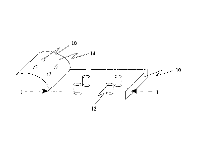
BRIEF DESCRIPTION OF THE FIGURES
5
FIG. 1A, FIG. 1B and FIG. 1C depict one aspect of a biochip of the present
invention. A substrate (10) made of appropriate material, such as fused
silica, glass, silica,
Si02, silicon, rubber, ceramics, PTFE, plastics, polymers or a combination or
combinations
thereof can define holes (12) that form ion transport measuring means, or at
least in part ion
transport measuring means, of the present invention. Optionally, a coating
(14) such as a
polymer coating can be placed on top of the surface of the substrate. The
coating can include
functional groups to aid in the localization and immobilization particles at
or near the holes
(12). Such functional groups can include, for example, specific binding
members that can
facilitate such localization or immobilization of particles. The coating can
also define holes
(16) that can functionally engage the holes (12) defined by the substrate
(10). In one aspect
of the present invention, such holes (16) in the coating (14) are preferable
because the
accuracy and precision for machining or molding such holes in the coating is
better suited for
the coating (14) rather than the substrate (10). For example, it is more
efficient, accurate and
precise to manufacture holes in the thin coating (14) rather than the
relatively thick substrate
(10). This is particularly true when the coating (14) is made of polymers
whereas the
substrate (10) is made of harder materials that may be less suitable for
machining, etching or
molding, such as silica. FIG. 1A depicts a biochip of the present invention
with a coating.
FIG. 1B depicts a cross section of FIG. 1A along "1-1" showing the coating in
place. FIG.
1C depicts a biochip not having a coating. Although cylinder-shaped holes (12)
are depicted
in FIG. 1A ¨ FIG. 1C, the holes can be of any regular or irregular geometry,
as long as the
holes, with or without the coating (14), allow adequate electric seals or
electronic seals (high
resistance seals, for example, mega ohms and giga ohms) between the membranes
of the
particles (for example cells, artificial vesicles, cell fragments) and the
substrates or the holes
for appropriate electrophysiological measurement of ion transports located in
the membranes.
For example, in the cross sectional view depicted in FIG. 1A and FIG. 1C, the
holes (12) do
not have to be vertically straight and can have a funnel shape, as shown in,
for example, FIG.
2B. The coating (14) depicted in FIG. 1A and FIG. 1B may be the same or
similar material
as the substrate (10). For example, the coating (14) can be a functionalized
surface having
appropriate, hydrophilicity or hydrophobicity, texture (for example,
smoothness) and/or
CA 02485099 2004-11-02
WO 03/093494
PCT/US03/14000
6
composition, for facilitating or enhancing high-resistance sealing (for
example electric seals
or electronic seals) between the substrates or holes and the membranes of the
particles under
electrophysiological measurement. Examples of the coating materials include
glass materials
and silicon dioxide deposited on the substrate by different methods such
chemical vapor
deposition and physical vapor deposition (e.g. sputtering or evaporation).
FIG. 2 depicts different configurations of substrates (10) and coatings (14)
to form
holes in the substrate (12) and holes in the coating (16). FIG. 2A depicts the
biochip of FIG.
1A with a cell (24) engaged thereto. FIG. 2B depicts a substrate (10) with a
coating (14),
wherein the substrate has been machined or etched to form a funnel shaped
structure (20).
This funnel shaped structure (20) can allow for less rigorous manufacturing
parameters as
compared to the straight walled holes (12) depicted in FIG. 2A. A cell (24) is
depicted
'engaged on the structure of FIG. 2B. FIG. 2C depicts the structure of FIG. 2B
inverted with
a cell (24) engaged thereto. FIG. 2D depicts a structure having a double
funnel structure (20,
22) that defines a hole (12) in the substrate (10). FIG. 2E depicts a
substrate (10) with a
smaller hole (12) with a funnel structure (20) engaged with a cell (24) with
electrodes (60,
61) placedon alternate surfaces of the biochip. Although holes of particular
shapes and
dimensions are depicted, the holes can be of any appropriate shape or
dimensions. Shapes of
holes can be geometric or non-geometric, such as circular, oval, square,
triangular,
pentagonal, hexagonal, heptagonal, octagonal or the like. Non-geometrical
shapes such as
kidney bead or other shapes are also appropriate. Geometric shapes can have
the advantage
of allowing higher density packing of holes, such as in a honeycomb
configuration. The
diameter or cross section of the holes at the portion where a particle is
contacted can be of
any appropriate size, but is preferably between about 0.1 micrometer and about
100
micrometers, more preferably between about 0.5 micrometer and about 10
micrometers, most
preferably between about 0.8 micron and about 3 micrometers. The diameter of a
hole refers
to the minimum diameter value if the hole changes in size along its length
direction.
FIG. 3 depicts a variety of particle positioning means provided on a biochip
of the
present invention. The particle positioning means can be provided on the
surface of the
substrate, coated by a coating or be imbedded within the substrate. FIG. 3A
depicts a
quadrople electrode structure or electrorotation structure (30) useful for
positioning particles
(35) at or near a hole (12, 16) wherein the electrical connection leads (37)
thereto are
operably connected with an AC signal source (for example, an electrical signal
source) (32),
such as a sine wave generator (which can also provide signals other than sine
waves), to
CA 02485099 2004-11-02
WO 03/093494
PCT/US03/14000
7
allow modulation of current at the electrode structures and/or to produce an
electric field in
the regions between and close to the electrode structure (30) to allow
positioning of particles
(35). FIG. 3B depicts a spiral electrode structure (34), circular in nature,
that is useful for
positioning particles (35) at or near a hole (12, 16) wherein the depicted
electrical connection
leads (37) are operably engaged with an AC electrical signal source (32). The
number of
spiral electrode structures is preferably three or more, and more preferably
between about
three and about ten. The electrode structures are preferably parallel at the
tangent. FIG. 3C
depicts a concentric electrode structure (36), circular in nature, that is
useful for positioning
particles (35) at or near a hole (12, 16) wherein the depicted electrical
connection leads (37)
are operably engaged with an AC electrical signal source (32). FIG. 3D depicts
a square
electrode structure (38), square in nature, that is useful for positioning
particles (35) at or near
a hole (12, 16) wherein the depicted electrical connection leads (37) are
operably engaged
with an AC electrical signal source (32). FIG. 3E depicts an electromagnetic
electrode (31),
that is useful for positioning particles (35) having bound thereto a magnetic
microparticle
(39) at or near a hole (12, 16) wherein the depicted electrical connection
leads (37) are
operably engaged with an electrical signal source (32). The electrical signal
source connected
to electromagnetic electrodes or electromagnetic structure is preferably an AC
or DC
electrical current source (for example DC power supply). Nevertheless, AC or
DC electrical
voltage source may also be used. FIG. 3F depicts a traveling wave
dielectrophoresis
structure (33), that is useful for positioning particles (35) at or near a
hole (12, 16) wherein
the depicted electrical connection leads (37) are operably engaged with an AC
electrical
signal source (32). FIG. 3G depicts a biochip wherein electromagnetic
structures (35) are
provided on or within a biochip. Preferably, the electromagnetic structures
are within the
biochip. FIG. 3H is a cross section of the biochip of FIG. 3G along 3-3. Also
shown are
particles such as cells (24) engaged with the holes (16) that can be coupled
or linked to a
magnetic particle (39-1, 39-2) of small (39-1) or large (39-2) size.
FIG. 4 depicts a particle switch (40) that can modulate the direction of
travel of
particles of different dielectric properties (42, 44) along a path and through
a particle switch
when the electrodes in the particle switch are connected to and applied with
an AC electrical
signal source. The particle switch can include holes (12, 16) for use as ion
transport
measuring means, or at least in part as ion transport measuring means. A
sample can include
a mixture of target particles and non-target particles. Target particles are
preferably separated
from or enriched from the non-target particles prior to measurements.
CA 02485099 2004-11-02
WO 03/093494
PCT/US03/14000
8
FIG. 5 depicts a structure such as depicted in FIG. 2B including a substrate
(10) that
defines a hole (12) with a funnel structure (22). FIG. 5A depicts such a
structure with a
coating (50) over all surfaces. The coating can be made of appropriate
materials, such as
polymers or functional coatings that can allow for immobilization of materials
such as
biological moieties or chemical moieties. The coating can also include binding
members,
such as specific binding members, such as antibodies, that can facilitate the
localization or
immobilization of particles such as cells at or near the hole (12). In one
aspect of the present
invention, the coating is made of a polymer that has the characteristic of
changing size with
temperature. By changing in size (e.g., increasing or decreasing), the polymer
can promote
the formation of an efficient seal between a particle (24) such as a cell and
the hole. In
another aspect of the present invention, the substrate can be of any suitable
material that
provides a surface, including but not limited to one or more plastics,
ceramics, metals, fibers,
polymers (e.g., polyimide, polyamide, polycarbonate, polypropylene, polyester,
mylar,
teflon), silicon, silcon dioxide, or glass, and the coating can be a glass
coating, silicon, silicon
dioxide, that is deposited on the top of the substrate. The glass can
optionally be further
treated, for example, with chemicals or by baking or polishing, to improve its
electronic
sealing properties. In FIG. 5B the coating (52) is depicted as being localized
to an area in
close proximity to the hole (12) in the substrate. In one aspect of the
present invention, the
coating in this configuration includes specific binding members present on
particles such as
cells. In FIG. 5C (54) the coating is depicted as being localized to the hole
(12) and
optionally surrounding areas. This configuration can promote a strong seal
(for example a
high resistance seal) between the cell and the hole (12). In one aspect of the
present
invention, the substrate (10) is made of silicon. The substrate (10) is then
heated to make a
structure that includes the substrate (10) of silicon and a coating (50) of
silicon dioxide. FIG.
5D depicts one aspect of the present invention where the coating (56) is
localized in the hole
and the surrounding areas on the bottom of the substrate (10). The coating
(56) is of material,
such as detergent or lipid binding proteins, preferably provided in a matrix
such as polymer
matrix that can dissolve or weaken membrane lipids or structure. As an
example, use of this
device to measure ion transport function or properties in eukaryotic cells
such as mammalian
cells, a cell is pushed or pulled into a hole (12) to achieve appropriate
electric sealing, for
example a 1 giga-ohm seal, between the cell membrane and the hole. When
membrane patch
of the cell is pushed or pulled down into the hole to be in contact with the
coating (56) the
lipid molecules in the membrane that are in contact or in close proximity with
the coating
CA 02485099 2004-11-02
WO 03/093494
PCT/US03/14000
9
(56) will dissolve or weaken by action of the coating (56). As a result, the
membrane patch
breaks off or is otherwise removed from the cell. This coating (56) serves as
a means to
rupture a membrane patch for certain whole cell ion transport assay methods.
As illustrated
here, the coating (50, 52, 54, or 56) of appropriate compositions may serve
different purposes
or functions such as promoting a strong seal (5C) between the cell and the
hole and rupturing
(5D) a membrane patch of the cell being assayed. Different coatings may be
employed for
different purposes. For example, the coating (for example, 54) may be
functionalized
surfaces having appropriate hydrophilicity or hydrophobicity, texture (for
example,
smoothness) and/or composition, which may facilitate and enhance high-
resistance sealing
between the substrates or holes and the membranes of the particles under
electrophysiological
measurement. Functionalized surfaces (for example 54) may be the same or
similar in
composition as the substrate (10), but with appropriate surface properties
such as smoothness
and electrical charge. The functionalized surfaces may be made by modification
of the
substrate, such as chemical modification or chemical treatment,by deposition
onto a surface
(such as, for example, by chemical vapor deposition (CVD), or by physical
vapor deposition
including, for example, sputtering and evaporation), or by coating a surface
(for example, by
spin coating). Those skilled in the art of microfabrication can readily choose
and determine
appropriate procedures and protocols for depositing or coating materials such
as glass, silicon
dioxide onto the substrates.
FIG. 6A depicts recording electrode structures (60, 61) present on either side
of a
hole (12) defined by a substrate (10) and depicted as including a funnel
structure (22). The
recording electrodes are positioned as to be on either side of particle, such
as a cell (24), or in
general to be at a certain distance from the particle (24). Electrical
connection leads (62)
connect the recording electrodes (60, 61) to a measuring device (63) (or a
recording circuit)
that can measure and optionally record the electrical properties of the
particle depicted by the
dashed line. For example, electric current through the ion transports in the
particle membrane
under applied voltage conditions can be recorded, or the cell membrane
potential can be
measured under fixed current flow through the ion transports in the membrane.
A measuring
device (63, or called "recording circuits") can be conventional
electrophysiological
measurement apparatus, such as those developed and commercialized by Axon
Instruments
Inc. In FIG. 6A, the recording electrode structures (60, 61) for measuring
electrical
properties or responses of the ion transports in the particle membrane are
fabricated on the
substrate (10) or are attached to the substrate (10) with other methods.
However, this is not a
CA 02485099 2004-11-02
WO 03/093494
PCT/US03/14000
requirement for the present invention. The recording electrode structures may
be on or
attached onto the substrate, or may be located outside the substrate, as long
as the measuring
electrode structures can be used for monitoring electrical responses of the
ion transports of
the particles under measurement. FIG. 6B depicts a variety of recording
electrode structures
5 as viewed from the top of FIG. 6A. In one aspect of the present
invention, the recording
electrode (60) can have any appropriate shape, such as square, circular or
semi-circular. The
electrode is preferably operably linked to at least one electrical connection
lead (62). In one
aspect of the present invention, there can be several recording electrodes,
preferably
independently attached to separate electrical connection leads so as to be
independently
10 addressable, that have different distances from a hole (12 as shown in
FIG. 6A) on which a
particle (24) such as a cell may be positioned or landed. Depending on the
conditions of a
particular method or the electrical parameter being measured, such as voltage
or current,
electrodes of different shapes, sizes or geometries can be utilized. Although
FIG. 6B is
viewed from the top of FIG. 6A, similar structures can be provided as
recording electrodes
(61) as viewed from the bottom of FIG. 6B. The recording electrodes (61) can
be provided
in or outside of the funnel structure (22) when present. The recording
electrodes can be of
various compositions. Preferably, the recording electrodes are made from
materials that have
a relatively stable or constant electrode/solution interface potential
difference. For example,
Ag/AgC1 composition has traditionally been the preferred material for the
recording
electrodes.
FIG. 7A depicts a process of the present invention wherein a particle (24)
such as a
cell engages a hole (12, 16) on a biochip of the present invention including a
substrate (10)
and recording electrodes (60, 61). The particle (24) has preferably been
localized at or near
the hole (12, 16) using particle positioning means (not shown, for example
those structures
shown in FIG. 3) on the substrate (10) of the biochip or using other particle
positioning
approaches such as a negative pressure generated in the hole (12, 16) from the
side of the
biochip other than that the particle (24) is situated in or positive pressure
on the same side of
the biochip that the particle is situated in. As depicted in FIG. 7B, once
engaged, a portion of
the particle (24) is moved into the space of the hole (12, 16) using
appropriate forces, such as
acoustic forces to push a portion of the cell (24) into the hole (12, 16) or
electroosmotic,
electrophoretic or negative pressure to pull a portion of the cell (24) into
the hole (12, 16) or
positive pressure to push a portion of the cell (24) into the hole.
Appropriate structures, such
as acoustic structures, electroosmotic structures, electrophoretic structures
or negative
CA 02485099 2004-11-02
WO 03/093494
PCT/US03/14000
11
pressure structures or positive pressure structures can be provided on or near
the biochip or a
chamber connected thereto to allow for operations thereof. A good seal (70,
for example, a
high resistance seal, for example 1 giga ohm or above) between the substrate
or coating
thereon and the cell is preferable. Depending on the electric parameters being
measured,
mega ohm or giga ohm sealing between the particle and the hole is preferred.
FIG. 7D
depicts the rupturing of the membrane of the cell using a pulse of force, such
as negative
pressure or positive pressure or electric field pulse. When the electric field
pulse over micro-
second to milli-second is applied, a strong electric field is applied to the
membrane patch in
the hole causing the rupture of the membrane. A negative pressure pulse would
result in a
ruptured membrane as well. The rupturing of the membrane patch allows for
direct electrical
access to the particle interior (for example cell interior) from the hole (12,
16), and this is
called "whole cell configuration or whole cell access". In such a case,
electrical voltage
applied to the recording electrode structures (60, 61) in contact to the two
ends of the hole
through the measurement solutions introduced into the regions surrounding the
biochip (for
example above and below the biochip in FIG. 7A) is directly applied to the
membrane of the
particle, thus applied to the ion transports located in the membrane. After
the membrane
patch of the particle (24) inside the hole is ruptured, a good seal (70)
between the substrate or
coating thereon and the particle (for example a cell) is preferably maintained
during the
measurement of the ion transports. Electrical responses or electrical
properties of the ion
transports located in the membrane of the particle can be measured or detected
by using
various recording circuits, which may include a patch clamp amplifier. The
recording of the
ion transports under the whole cell configuration is typically called "whole
cell recording".
The good seal (for example high resistance seal, for example > 1 giga ohm)
ensures that the
electrical current from the ion transports' activity can be accurately
measured with only small
background leakage current. FIG. 7C depicts the case in which the membrane
patch of the
particle (24) located in the hole (12, 16) is not ruptured. In such a case,
the ion transport(s) in
the membrane patch of the particle located in the hole (12, 16) can be
measured. Such
measurement provides property information of one or a few ion transport
molecules in the
membrane patch and is sometimes referred as "cell-attached patch" recording.
FIG. 7E
depicts the case in which the membrane patch of the particle (24) located in
the hole (12, 16)
is not ruptured, but the electrical access of the particle interior is
achieved by permeabilizing
the membrane patch by using "membrane perrneabilization molecules or
reagents". In this
way, the pores (as alternate pathways for the movement of ions and electrons)
are formed in
CA 02485099 2004-11-02
WO 03/093494
PCT/US03/14000
12
the membrane patch and electrical voltages can, also be applied to the ion
transports on the
membrane of the particle (other than those in the membarne patch), and
electrical recording
of the ion transports can be performed in similar fashion to that for FIG. 7D.
FIG. 8 depicts a structure of the present invention that includes protrusions
or wires
(80) that can be singular, partially circumnavigate or circumnavigate with
regard to the hole
(12, 16). The use of these structures is depicted in FIG. 9.
FIG. 9 depicts the operation of the structure depicted in FIG. 8 or FIG. 15.
In FIG.
9A, a particle (24) such as a cell is engaged with the protrusions (80). This
is preferably
accomplished by applying a positive or negative force, such as depicted in
FIG. 7. The area
of membrane bound in the hole, is ruptured, such as through a pulse of force,
to form a whole
cell configuration. The electrical connection leads (62) from the recording
electrodes (60,
61) connect to a measuring device (63) or a recording circuit that can monitor
and optionally
record the electric properties or electrical current in the circuit completed
as depicted by the
dashed line.
FIG. 10 depicts one preferred aspect of the present invention. In cross
section a
substrate (10) with a coating (14) is shown with a hole (12) in the substrate
and a hole (16) in
the coating with a funnel structure (22) and fitted with recording electrodes
(60, 61). Also
depicted are particle positioning means (100), which in this case are depicted
as traveling
wave dielectrophoresis structures (100).
FIG. 11 depicts one aspect of the present invention wherein wells (110) are
formed
on a substrate (10). The wells can be of any appropriate shape, such as but
not limited to the
circles and squares depicted. The wells can be fabricated using appropriate
methods, such as
a machining or etching. The wells preferably, but optionally, include particle
positioning
means (112). The wells are reminiscent of wells of a microtiter plate, but are
preferably
, 25
much smaller. In this way, a particle or population of particles, such as
cells, can be added
into the well or wells using introduction or dispensation methods and
technologies
appropriate for the type of particles being used. Also, appropriate
introduction or
dispensation methods and technologies can be used to deliver reagents, such as
test reagents,
to the wells. Appropriate delivering methods include piezo dispensers, ink jet
technologies,
pip etters, micropipetters, electrophoretic dispensations, connected tubings,
other
microfluidics methods and devices and the like, such as they are known in the
art or later
developed. For example, the introduction methods could be realized through
microfluidic
channels in which electroosmotic pumping or pressure driven pumping of the
fluid is utilized.
CA 02485099 2012-12-06
13
Such electroosmotic pumping or pressure driven pumping of the fluid can be
used not only for
delivering and dispensing reagents and test solutions, but also for
positioning particles to or
near the ion transport measuring means on the chip. A number of examples of
traveling wave
dielectrophoretic structures, that can be used for transporting particles to
the ion transport
measuring means, are provided herein and in United States patent number
6,596,143.
FIG. 12 depicts one preferred aspect of the present invention that includes
particle
separation structures along with particle positioning means. In this figure, a
substrate (10) is
fitted with traveling wave dielectrophoretic structure (120) that can separate
particles (122,
124) of differing dielectric properties and/or other properties, such as live
cells (122) and dead
cells (124) which can be visualized using trypan blue exclusion or other
viability dyes. The
separated cells (126) are subject to one or more particle positioning means,
such as a particle
switch (128) which can further separate members of a population of cells
(122,124) and direct
the desired population of cells to an ion transport measuring means (121). The
cell directed to
the ion transport measuring means is then engaged therewith for ion transport
functional
analysis.
FIG. 13 depicts one preferred aspect of a flow through method for engaging
particles
such as cells (24) with ion transport measuring means (138). The depicted
structure includes a
channel (130), but the method depicted in FIG. 13 can be utilized on a biochip
that does not
include such channels (130). Particles such as cells (24) are positioned at or
near ion transport
measuring means (138) using particle positioning means (132) depicted here as
traveling wave
dielectrophoresis structures. The cells (24) engage the ion transport
measuring means (138)
and allow for detection on ion transport function or properties via measuring
devices (131) or
recording circuits that can provide a readout (133). Samples (134) can be
sequentially added to
the biochip, such as through the channel (130) with or without dye solutions,
reagent solutions
including substrates (such as for enzymes), enzymes, or cells and the like, or
washing
solutions (136) in between the samples. The samples are sequentially contacted
with the cells
(24). The same cells can be tested with a given set of compounds. The
modulation of ion
transport function or properties in response to these compounds is
interrogated using ion
transport measuring means (138), and the responses measured (131) and/or
reported (133).
Here, compounds I, II and IV increased ion transport function or properties
whereas
compound III did not.
CA 02485099 2004-11-02
WO 03/093494
PCT/US03/14000
14
FIG. 14 depicts one aspect of the present invention wherein a substrate (10)
with one
or more holes (16) is provided in a chamber (140) (or a cartridge 140) with an
upper
compartment (142) and a lower compartment (144) separated by a substrate layer
with the
holes. The holes (16) can be part of an ion transport detection or measuring
structure.
Capillaries or needles of the present invention can also be present or be
substituted for the
holes (16). The substrate (10) can include a variety of particle positioning
means, particularly
horizontal positioning means, such as but not limited to electromagnetic
devices and
dielectrophoretic devices (not depicted). The chamber or cathidge (140) can
include various
particle positioning means, particularly vertical particle positioning
structures, such as
electrOphoretic elements (146), acoustic elements (148), electroosmosis
elements (141) and
pressure control elements (143). In operation, a sample that includes a
particle such as a cell
can be introduced into the chamber or cartridge (140) by way of a conduit
(145). The particle
is positioned at or near the hole (16) by way of horizontal positioning
structures. The particle
is then aligned with the hole (16) using vertical positioning structures. The
electric seal (70)
between the particle and the hole can be enhanced using coatings, such as
coatings including
specific binding members or particle adhesion moieties, such a cell surface
adhesion proteins,
such as integrins or basement membrane proteins such as fibronectin. Other
methods for
enhancing the electric seal (70) between the particle and the hole can also be
used. For
example, chemical modification or treatment of the hole may be used to alter
the hole surface
properties, for example, surface smoothness and/or surface compositions so
that the altered
surface properties allows better electrical seals (for example, higher
resistance seal, shorter
time to seal, more stable seal) between the particle and the hole. The
particle can then be
optionally ruptured, such as by the vertical positioning means such as
pressure pulses.
Preferably, the pressure control element (143) performs this function, but
that need not be the
case. Alternatively ion-conducting holes can be made in the membrane by
perforating agents
such as but not limited to amphotericin B. At this point in time, ion
transport functions or
properties of the particle can be determined using methods of the present
invention. In one
aspect of the present invention, test compounds can be introduced via the
inlet port (145) and
effluent can be removed via the effluent port (147) or outlet port.
FIG. 15 depicts the fabrication of a capillary of the present invention that
can be used
as an ion transport detection or measuring structure in a manner generally
depicted in FIG. 9.
The process starts with providing a substrate (10), which is then etched to
form protrusions
(150) that will form a capillary structure (152). This etching forms a trench
(154) that defines
CA 02485099 2004-11-02
WO 03/093494
PCT/US03/14000
the protrusion (150) or capillary (152). Particles such as cells may engage
onto such capillary
(152) in similar ways or formats to that when cells engage onto conventional
glass pipettes
for patch clamp recording. Further etching from the other side of the
substrate forms a hole
(16) that can have a funnel shape. Deposition (for example sputtering) and
photolithographic
5 processing of conductive material can be used to provide electrode
structures (61) for use in
ion transport function or properties determinations using methods of the
present invention. In
one aspect of the present invention, the protrusion (150) can be hollow and be
open or closed
at the top of the structure.
FIG. 16 depicts the manufacture and use of needle structures for ion transport
10 function or transport determinations. FIG. 16A depicts the manufacture
of such a structure.
A substrate (10) is provided, upon which a conductive material (160) is
provided using, for
example, sputtering, chemical growth, electrochemical growth or other growth
methods. The
conductive material provides an electrode portion (166) operably connected to
a needle
structure (164). Optionally, a button (162) of conductive material can be
added to the
15 electrode portion (166) via sputtering. An insulating material (168)
such as SI02 or Si3N4 or
a polymer material (for example a resist) is then added over the conductive
material (160) via
sputtering, evaporation or other appropriate methods. Photolithographic
methods and other
patterning techniques can be used for these procedures. Excess insulating
material is then
removed by appropriate methods such as masked etching which results in a
needle structure
of the present invention (161). The needle structure of the present invention
has an
electrically conductive tip that is connected to the recording electrode
structure (162B) on the
substrate and an insulator surface that covers the rest part of the needle
structure. In general,
the conductive tip is less than 10 microns in length. Preferably, the
conductive tip is less than
5 micron. More preferably, the conductive tip is less than 2 micron.
Electrical measurements
can be made between the recording electrode (162A) and the needle structure
(161) as
depicted by dashed lines. The needle structure can be connected to electrical
connection
leads (162) using appropriate methods, such as sputtering of conductive
material at
appropriate times during the manufacture of the device. Those skilled in micro
fabrication
can choose appropriate protocols and materials for making these devices. FIG.
16B and
FIG. 16C depicts the use of the device of FIG. 16A in an ion transport
function or property
determination. The needle structure (161) is contacted with a sample including
a particle (24)
such as a cell. The cell is positioned at or near the needle structure such as
by horizontal
positioning structures (not depicted). The particle is then impaled upon the
needle structure
CA 02485099 2004-11-02
WO 03/093494
PCT/US03/14000
16
such as by vertical positioning structures (not depicted). As depicted in FIG.
16A, the needle
structure has a conductive tip and an insulator surface covering the rest part
of the needle
structure. When the particle is then impaled upon the needle structure, the
conductive tip of
the needle structure is fully inside the particle interior so that the needle
structure engages the
particle surface (for example cell membrane) at the insulator-covered regions
of the needle
structure. The electric seal between the particle and the needle structure or
the insulator-
covered region of the needle structure, can be enhanced using specific binding
members at a
location corresponding to the juncture of the particle with the needle
structure. Similar to the
cases for other ion transport measuring or detection structures (for example a
hole 12, 16 in
FIG. 7), the electric seal or sealing between the particle and the needle
structure here refers to
the high resistance engagement of the particle surface (for example cell
membrane) to the
insulator-covered region of the needle structure so that the electrical
leakage from the particle
interior to the spaces outside and surrounding the particle through the
regions at the particle
surface-needle structure interface is minimized. Ion transport function or
property
determinations can be made using methods of the present invention by measuring
the
electrical properties between the recording electrode (162A) and the needle
structure (161) as
depicted by the dashed line which completes the depicted circuit that includes
an electrical
measuring device (172) or a recording circuit that may include an electrical
source (174).
Specific patterning methods such as photolithography can be used for producing
recording
electrode structures (160) at locations on the substrate (FIG. 16A and 16B).
FIG. 17 depicts a chip (180) of the present invention that includes an array
(182) of
long-range (184) and short-range (186) particle positioning means around a
hole on a chip
optionally within a chamber or a cartridge (188). Each depicted unit in the
array is a
measurement unit. Short-range particle positioning means are most effective at
a range of
less than about 60 micrometers, more typically less than about 40 micrometers.
Long-range
particle positioning means are most effective at a distance of between greater
than about 30
micrometers and less than about 10 centimeters, typically between greater than
about 40
micrometers and less than about 1 centimeter or about 5 millimeters. In
operation, the long-
range (184) particle positioning means are used to localize a particle such
that the short-range
(186) particle positioning means can localize the particle within a range
(181) at the hole
(183) such that ion channel determinations can be made. In the instance
depicted, the long-
range (184) and short-range (186) particle positioning means operate on
dielectrophoresis
principles. In certain aspects of the present invention, the top chamber can
be a single
CA 02485099 2004-11-02
WO 03/093494
PCT/US03/14000
17
chamber for all of the measurement units, or the top chamber can be multiple
discrete units.
Such multiple discrete units can engage one or several particles in each unit,
depending on
the number of holes (or ion transport measuring or detection structures)
provided in each unit.
In the aspect where there are individual cells in a measurement unit, then the
bottom chamber
can be separate and discrete for each measurement unit so that microfluidics
or fluidic
devices using pumps, valves, tubing and the like can be individually monitored
and
manipulated, and individual recording electrodes and electrical connection
leads can be
provided. Although the long-range and short-range particle positioning means
are depicted
as the same configuration in this figure, different configurations can be
utilized and can be
designed depending on the conditions, target particles and assays to be
performed. In the
cartridge (188) depicted in FIG. 17, the top chamber (or top fluidic
compartment) has one
inlet port and one outlet port, and the bottom chamber (or bottom fluidic
compartment) has
one inlet and one outlet port. Through these inlet/outlet ports, the cartridge
or chamber (188)
is connected to external fluidic devices such as tubing, pumps, valves so that
measurement
solutions, cell suspensions, reagents, test compounds can be delivered to or
withdrawn from
the top and bottom chambers of the cartridges. Typically, the solutions
delivered to the top
chamber (or top fluidic compartment) comprises cells, extracellular solutions
and/or testing
compounds for extracellular usage and the solutions to the bottom chamber (or
bottom fluidic
compartment) comprises intracellular solutions and/or testing compounds for
intracellular
use, but this need not be the case. In alternative arrangements, the top
chamber (top fluidic
compartment) can be used as intracellular chamber loaded with intracellular
solutions and/or
testing compounds for intracellular use whilst the bottom chamber can be used
as
extracellular chamber for introducing a sample comprising particles. For
example, various
external fluidic devices such as valves, pumps, and solution reservoirs (not
shown) can be
used to perfuse the top chamber after the cell is engaged onto the hole (183)
with high
resistance so that the response of ion transports in the cell membrane to
various testing
compounds can be monitored, measured and/or recorded. For the measurement of
ion
transports using chips and cartridges shown in FIG. 17, recording electrodes
(not shown)
that are in contact with the top and bottom chambers and are connected to the
recording
circuits are needed. The recording electrodes may be integral to the chip so
that the recording
electrodes are fabricated on the chip. Alternatively, the recording electrodes
may be on or
within the chip.
CA 02485099 2004-11-02
WO 03/093494
PCT/US03/14000
18
FIG. 18 depicts a modified configuration from that depicted in FIG. 17. FIG.
18
depicts a cartridge (199) comprising structures (190) being formed by a top
fluidic channel
(192, or top fluidic compartment) and a bottom fluidic channel (194, or bottom
fluidic
compartment) that can be made using appropriate methods such as etching,
machining or
polymerization. The fluidic channels or fluidic chambers (192, 194) are
preferably closed,
but can also be in an open configuration, in particular the fluidic channel
that holds
extracellular solution, in this case, the top fluidic channel (192). The
fluidic channels are
separated by a biochip (196) that comprises ion transport measuring structure
such as a hole
(195) and are preferably provided on a substrate (198). Particle positioning
means (191) can
be present to guide a particle, such as a cell (193), to an ion transport (for
example, ion
channel) measuring structure, such as a hole (195). FIG. 18B depicts a
cartridge comprising
9 measurement units. Each unit comprises a hole or aperture (195) as an ion
transport
measuring means, a top fluidic chamber or channel (192) and a bottom fluidic
channel or
chamber (194). As shown in FIG. 18B, the bottom fluidic channel or chamber
(194) has two
ports (for example one inlet and one outlet fluidic port) whilst the top
chamber (192) was in
the open configuration. The top chamber or channel may also be in a closed
configuration
with one inlet and one outlet port. For the measurement of ion transports
using biochips and
cartridges shown in FIG. 18, recording electrodes (not shown) that are in
contact with the top
chamber (192) and bottom chamber (194) and are connected to the recording
circuits are
needed. The recording electrodes may be integral to the chip so that the
recording electrodes
are fabricated on the chip. Alternatively, the recording electrodes may be on
or within or near
the chip.
FIG. 19 depicts a top view of a biochip of the present invention where the
aperture or
hole for ion channel or ion transport detection or measurement is provided on
the side of a
fluidic channel rather than through the substrate. Additional particle
positioning means
besides the special confinement by the channels for this type of patch-clamp-
in-a-channel
technology can be provided near the hole, but is optional.
FIG. 20 depicts a cross section of one aspect of an ion transport recording
chip
depicted in FIG. 19 where the method of manufacture is diagrammatically shown.
In one
aspect of the present invention, a conduit is made using sacrificial layer
methods. One
preferred method is wire sacrificial methodologies such as they are known in
the art, such as
by the use of a copper wire. Photoresist can also be used for sacrificial
layers.
CA 02485099 2004-11-02
WO 03/093494
PCT/US03/14000
19
FIG. 21 depicts a multi-functional biochip useful for high information content
screening. Samples are provided at port (400). Particles in the sample are
transported and
optionally separated along a fluidic channel (410) that can include particle
manipulation
means such as dielectrophoretic structures. Particles can be transferred from
the port to the
first chamber by fluidic devices or particle manipulation means, including,
for example,
dielectrophoresis structures, traveling wave dielectrophoresis structures,
etc., or devices that
use pressure or gravity flow of fluids, etc.. A first chamber (or well) (420)
is provided, which
in the depicted configuration performs a cell viability test, such as a dye
exclusion test where
the results are detected by optical means. (Any appropriate test can take
place in the first
chamber, but the viability test is depicted forillustrative purposes.) A
second fluidic channel
can connect the first chamber to other chambers where other tests can be
performed. For
example, the cells in the first chamber can be transported to an ion transport
detection unit
(430) or other units, such as fluorescent units (450), genomics units (460) or
proteomics units
(440). The ion transport unit includes ion transport detection structures as
described herein,
in particular as depicted in, for example, FIG. 17, FIG. 18, FIG. 19 or FIG.
20. Optional
particle separation units can be provided within, or after each chamber or
units that performs
detection functions.
FIG. 22A shows an SEM (scanning electron microscopy) image of the backside
opening on a silicon biochip for ion transport measurement and detection. FIG.
22B shows
an SEM image of an ion transport measurement aperture or hole fabricated on
the front side
of a silicon biochip.
FIG. 23A and 23B shows the cross-sectional SEM images of ion-transport or ion-
channel measurement holes made on silicon substrates prior to the oxidation
and after
oxidation. FIG. 24 shows a microscopic image of an ion transport measurement
hole (or an
ion channel recording hole) surrounded by a quadropole electrode structure for
particle
positioning.
FIG. 25 shows a schematic representation of the laser ablation used to make
ion
transport measurement holes or ion channel recording holes on a solid
substrate (for example
glass).
FIG. 26 shows SEM images of counter-pore (A) and entrance hole (A) and exit
hole
(B) for a glass biochip produced using laser ablation. FIG. 26C shows an SEM
image of two
counter-pores and entrance hole for a glass biochip with double counter-pore
configuration.
CA 02485099 2004-11-02
WO 03/093494
PCT/US03/14000
FIG. 27 shows an example of the current recorded in response to a voltage step
(from
¨70 mV to ¨60 mV, pulse width of 50 ms) for a RBL-1 cell engaged with a hole
on a silicon
wafer based chip that has been deposited with a layer of Borosilicate glass.
FIG. 28A and B shows a comparison for the whole cell currents for two RBL-1
cells
5
recorded using a conventional patch-clamp glass capillary electrode (panel A)
or a biochip
made from SOT (silicon-on-insulator) wafer (panel B).
FIG. 29 shows the whole cell recording from an RBL-1 cell using a glass
biochip for
a voltage ramp protocol. The glass chip was baked at 570 C for about 1 h and
stored in de-
ionized H20 for about 2 hrs.
10
FIG. 30 shows the whole cell recording from an RBL-1 cell obtained with a
conventional patch clamp glass capillary electrode.
FIG. 31 shows the whole cell recording from an RBL-1 cell using a glass
biochip
FIG. 32 shows an exemplary whole-cell recording for a R_13L-1 cell recorded on
a
glass chip, that was baked
15
FIG. 33 shows an exemplary whole-cell recording from an RBL-1 cell recorded on
a
glass biochip without baking treatment FIG. 34 shows an exemplary whole-cell
recording for
a RBL-1 cell recorded on a glass chip that was laser-polished on the side of
chip surface
corresponding to the extracellular chamber.
FIG. 35 shows the microscopic images of a 150 micron dielectrophoresis
positioning
20
structure. FIG. 35A shows the electrodes (light region) and the interelectrode
spaces (dark
region). FIG. 35B shows the ion transport measuring hole in the central region
of the
interelectrode space.
FIG. 36 shows the whole cell recording of a RBL-1 cell on a glass biochip
after the
cell was positioned with dielectrophoretic forces followed by a slight
negative pressure
applied to the ion transport recording hole from the bottom chamber
(alternatively, a slight
positive pressure can be applied to the hole from the top chamber).
FIG. 37A and 37B show the photographic images of various cartridges for
testing ion
channel biochips.
FIG. 38 shows a diagram of a cartridge that is operated isuch that the
intracellular
chamber is on the top of the biochip and the extracellular chamber now is
below the biochip
with hole opening downward from the top of the chamber.
FIG. 39 illustrates the principle of a method for addressing the problem of
relatively
low success rate in patch clamping.
CA 02485099 2004-11-02
WO 03/093494
PCT/US03/14000
21
FIG. 40 shows the schematic drawing for a cartridge having eight ion transport
recording wells.
FIG. 41 shows the schematic drawing for an ion-transport measuring/detection
system using a biochip having a plurality of ion transport holes/apertures.
Each hole is
connected to a top chamber (extracellular chamber) and a bottom chamber
(intracellular
chamber), respectively.
FIG. 42 shows the schematic drawing for an ion-transport measuring/detection
system using a biochip having a plurality of ion transport measurement holes.
A plurality of
the measuring holes share a bottom chamber (a common intracellular chamber)
whilst the
extraceullar chambers are separate from each other.
FIG. 43 shows the schematic drawing for an ion-transport measuring/detection
system using a biochip having a plurality of ion transport measurement holes.
A plurality of
the measuring holes share a top chamber (a common extracellular chamber)
whilst the
intraceullar chambers are separated from each other.
FIG. 44 shows the schematic drawing for a region of a biochip wherein the ion
transport measuring holes are integrated with dielectrophoresis electrodes
within microfluidic
channels.
FIG. 45 shows the schematic drawing for an ion-transport measuring/detection
device
using a fiber-optic tubing with pre-drilled patch clamp recording holes in a
configuration
where fiber-optic tubing is used in combination with multiple microfluidic
channels on a
substrate.
FIG. 46 shows a schematic drawing for an ion-transport measuring/detection
device
using fiber-optic tubing in a configuration where a fiber-optic tube is
inserted into another
larger tube, as part of a multiunit bundled fiber-optic tubing structure.
FIG. 47 shows the schematic drawing for electrophysiological read-outs for
GPCR
assays by using G-protein-coupled ion channels.
FIG. 48 shows the schematic drawing for electrophysiological read-outs for
assays by
using ion channels activated or inactivated by the cellular intermediate
messenger systems as
a signal transducer between a cellular receptor/ligand binding event
(including both plasma
membrane receptors and intracellular receptors) and an ion channel effector
read-out.
FIG. 49 shows the schematic drawing for electrophysiological read-outs for
assays
using ion channels as reporter genes.
CA 02485099 2004-11-02
WO 03/093494
PCT/US03/14000
22
SUMMARY
The present invention recognizes that the determination of ion transport
function or
properties using direct detection methods, such as patch-clamp, whole cell
recording or single
channel recording, are preferable to methods that utilize indirect detection
methods, such as
fluorescence-based detection systems. The present invention provides biochips
and other
fluidic components and apparatuses and methods of use that allow for the
direct analysis of
ion transport function or properties using microfabricated structures that
allow for automated
and/or high throughput detection of ion transport functions or properties.
These biochips and
fluidic apparatuses and methods of use thereof are particularly appropriate
for automating the
detection of ion transport function or properties, particularly for high
throughput screening
purposes.
A first aspect of the present invention is a biochip comprising at least one
particle
measuring means and methods of use. The biochip preferably includes at least
one particle
positioning means and at least one ion transport measuring means. The particle
positioning
means is preferably active upon cells such as eukaryotic cells using
appropriate forces,
particularly dielectric forces and hydrostatic pressure. The ion transport
measuring means
can be any appropriate ion transport measuring means, such as but not limited
to structures
that can be used for patch clamp detection, whole cell detection or recording,
single ion
transport detection or recording, and the like.
A second aspect of the present invention is an array of capillaries on a
biochip and
methods of use. The array of capillaries is preferably microfabricated and
integrated onto the
chip such that they are useful in ion transport function determinations. In
one aspect of the
present invention, the capillaries can be used as ion transport measuring
means in patch
clamp assay methods, whole cell assay methods, or single channel assay
methods.
A third aspect of the invention is an array of needle electrodes on a biochip
and
methods of use. The array of needle electrodes is preferably microfabricated
such that they
are useful in ion transport determinations. These structures are particularly
useful in ion
transport determinations using whole cells.
A fourth aspect of the invention is an array of holes on a biochip and methods
of use.
The holes are preferably microfabricated and are useful in methods for the
determination of
ion transport functions or properties. The holes can be used in patch clamp
methods such as
whole cell or single ion channel methods. In one aspect of the present
invention, the holes
can be used in whole cell or single ion channel methods, particularly when
pressure is applied
CA 02485099 2004-11-02
WO 03/093494
PCT/US03/14000
23
upon a solution through such holes. In another aspect of the present
invention, the surface of
the substrate around and within the hole is capable of engaging particles such
as biological
cells, vesicles, and/or membrane organelles with a high resistance electric
seal. In another
aspect of the present invention, the surface of the substrate around and
within the hole is
capable of engaging particles such as biological cells, vesicles, and/or
membrane organelles
with a high resistance electric seal. In one particular embodiment, the
substrate or coating
material for the biochip is glass, one or more holes is fabricated using laser
ablation.
A fifth aspect of the invention is a biochip or fluidic component having ion
transport
measuring means being apertures with appropriate geometries and dimensions,
which are
located along the side walls of microfluidic channels, and methods of use.
This type of
patch-clamp-in-a-channel technology provides means of efficient simultaneous
recording on
and fluid delivery to a biochip of current invention.
A sixth aspect of the invention is a fluidic component that comprises at least
one tube
with tube walls comprising one or more holes less than 10 micron in diameter.
In one aspect
of the present invention, the fluidic component comprises a second tube
wherein a first tube
is inserted in the second tube and the first tube serves as one fluidic
compartment and the
second tubes serve as a second fluidic compartment, and the two fluidic
compartments are
connected via one or more holes. In another embodiment of this aspect of the
present
invention, the fluidic component comprises a substrate with a microfluidic
channel on the
substrate surface, wherein a tube is arranged substantially perpendicular to
the microfluidic
channel and is sealed onto the substrate so that the tube serves as one
fluidic compartment,
the microfluidic channel serves as a second fluidic compartment, and at least
one aperture on
the tube wall connects the two fluidic compartments.
A seventh aspect of the invention is a method for modifying at least a portion
of a
chip or substrate comprising at least one ion transport measuring means to
enhance the
electric seal of a particle or a portion thereof with an ion transport
measuring means. In one
aspect of the present invention, the chip or substrate comprising an ion
transport measuring
means is modified to become more smooth. In another aspect of the present
invention, the
chip or substrate comprising the ion transport measuring means is modified
chemically.
An eighth aspect of the invention is the substrates, biochips, cartridges,
apparatuses,
and/or devices comprising ion transport measuring means with enhanced electric
seal
properties.
CA 02485099 2004-11-02
WO 03/093494
PCT/US03/14000
24
A ninth aspect of the present invention is a method for storing the
substrates, biochips,
cartridges, apparatuses, and/or devices comprising ion transport measuring
means with
enhanced electrical seal properties.
A tenth aspect of the present invention is a method for shipping the
substrates,
biochips, cartridges, apparatuses, and/or devices comprising ion transport
measuring means
with enhanced electrical seal properties.
An eleventh aspect of the present invention is a method for utilizing ion
transport
measurements as detection systems for a number of cell-based assays.
A twelfth aspect of the present invention is a method of using G-protein-
coupled ion
channels for electrophysiological read-outs for GPCR assays. In one embodiment
of this
aspect of the present invention, cellular intermediate messenger systems that
activate or
inactivate ion channels act as signal transducers between a cellular
receptor/ligand binding
event (including both plasma membrane receptors and intracellular receptors)
and an ion
channel effector read-out.
A thirteenth aspect of the invention is a biochip or a fluidic component with
at least
one ion transport measuring means combined with high information content
screening and
methods of use. This type of on-chip procedural combination allows for high
throughput
detection of multiple cellular signals in a time and space-controlled manner
that cannot be
achieved by existing technologies.
A fourteenth aspect of the invention is a biochip with three-dimensionally
configured
channels that can be microfabricated using sacrificial methodologies such as
sacrificial wire
methods and methods of use. This biochip provides a system of three-
dimensional
microfluidic structures that can be efficiently microfabricated for use in
high-density
bioassays and lab-on-a-chip systems.
The particle positioning means employed in the apparatuses, cartridges,
biochips,
methods, and systems of the present invention, particularly those used for
positioning
biological cells in an array format for single cell analysis, can be used with
significant
advantages for cell-based assays over current cell-based assays. Current cell-
based assays
analyze and examine a population of cells by measuring averaged, integrated
signals and do
not allow for assays at the single cell level. The cell positioning means
disclosed in this
invention provides the devices and methods for analyzing individual cellular
events in high
throughput formats. These analyses can be performed by reading out electrical
(for example,
ion transport assay) and optical (for example, fluorescent readout) signals
from individual
CA 02485099 2004-11-02
WO 03/093494
PCT/US03/14000
cells. Using the high throughput capability for ion transport assays in this
invention, one can
analyze the effects of intracellular signaling events on ion transport
functions or properties in
a systematic fashion. High throughput proteomics and functional analysis of
ion channels
can be performed at the single cell level. Furthermore, the devices and
methods in the
5 present invention allow the electrophysiological measurement of native
cells isolated from
tissues (normal or diseased). Such analysis would allow for a fast and more
accurate
determination for cellular variation as hundreds or thousands of cells could
be investigated
individually in parallel for their biological, pharmacological and
physiological responses.
Cellular variation has proven to be a factor complicating the scientific
analysis of complex
10 systems, for example, in the diseases such as arrhythmias, cancer, and
nervous system
disorders. The present inventions provide devices and methods to address such
cellular
variations by providing a multiplicity of single cell measurements in
parallel.
In addition, positioning of the individual cells in an array format may permit
better
studies in subcellular organization and microdomain measurements. With the
cells
15 positioned, dynamic subcellular locations of cellular compaitments,
structures and molecules
such as receptors and enzymes may be examined. Cells may be engineered to
express
recombinant ion channels or receptors with appropriate scaffolding proteins or
chaperone
proteins so that the surface expression of these proteins can be achieved at
certain locations in
a timed manner. For microdomain measurement of individual cells, various
detection
20 technologies such as optical measurements could be applied. Using the
methods and devices
of the present invention, individual cells can be positioned in an array
format and the
examination of hundreds or even thousands of the cells could be performed
using a single
device to assess their chemical and biochemical parameters or properties in
given subcellular
microdomains. These parameters include, but are not limited to, calcium
levels, enzyme
25 activity, translocation, membrane and molecular trafficking, pH, and
concentrations of
specific molecules.
DETAILED DESCRIPTION OF THE INVENTION
DEFINITIONS
Unless defined otherwise, all technical and scientific terms used herein have
the same
meaning as commonly understood by one of ordinary skill in the art to which
this invention
belongs. Generally, the nomenclature used herein and the manufacture or
laboratory
CA 02485099 2004-11-02
WO 03/093494 PCT/US03/14000
26
procedures described below are well known and commonly employed in the art.
Conventional methods are used for these procedures, such as those provided in
the art and
various general references. Terms of orientation such as "up" and "down" or
"upper" or
"lower" and the like refer to orientation of parts during use of a device.
Where a term is
provided in the singular, the inventors also contemplate the plural of that
term. The
nomenclature used herein and the laboratory procedures described below are
those well
known and commonly employed in the art. Where there are discrepancies in terms
and
definitions used in references that are incorporated by reference, the terms
used in this
invention shall have the definitions given herein. As employed throughout the
disclosure, the
following terms, unless otherwise indicated, shall be understood to have the
following
meanings:
"Dielectrophoresis" is the movement of polarized particles in electrical
fields of
nonuniform strength. There are generally two types of dielectrophoresis,
positive
dielectrophoresis and negative dielectrophoresis. In positive
dielectrophoresis, particles are
moved by dielectrophoretic forces toward the strong field regions. In negative
dielectrophoresis, particles are moved by dielectrophoretic forces toward weak
field regions.
Whether moieties exhibit positive or negative dielectrophoresis depends on
whether particles
are more or less polarizable than the surrounding medium.
A "dielectrophoretic force" is the force that acts on a polarizable particle
in an AC
electrical field of non-uniform strength. The dielectrophoretic force P DEp
acting on a particle
of radius r subjected to a non-uniform electrical field can be given, under
the dipole
approximation, by:
P DEP = 27C6 mr3 X DEP V E r2MS
where Ems is the RMS value of the field strength, the symbol V is the symbol
for gradient-
operation, cm is the dielectric permittivity of the medium, and
= v DEP is the particle
polarization factor, given by:
6 - m
X DEP = Re +P
6
P +2E,,,
"Re" refers to the real part of the "complex number". The symbol c: = ex ¨
jax/27if is the
complex permittivity (of the particle x=p, and the medium x=m) and j=-N -1.
The
CA 02485099 2004-11-02
WO 03/093494 PCT/US03/14000
27
parameters sp and up are the effective permittivity and conductivity of the
particle,
respectively. These parameters may be frequency dependent. For example, a
typical
biological cell will have frequency dependent, effective conductivity and
permittivity, at
least, because of cytoplasm membrane polarization. Particles such as
biological cells having
different dielectric properties (as defined by permittivity and conductivity)
will experience
different dielectrophoretic forces. The dielectrophoretic force in the above
equation refers to
the simple dipole approximation results. However, the dielectrophoretic force
utilized in this
application generally refers to the force generated by non-uniform electric
fields and is not
limited by the dipole simplification. The above equation for the
dielectrophoretic force can
also be written as
-.'*DEP =271-6 mr3 Z DEP V2 V p(x,y,z)
where p(x,y,z) is the square-field distribution for a unit-voltage excitation
(Voltage V = 1 V)
on the electrodes, V is the applied voltage.
"Traveling-wave dielectrophoretic (TW-DEP) force" refers to the force that is
generated on particles or molecules due to a traveling-wave electric field. An
ideal traveling-
wave field is characterized by the distribution of the phase values of AC
electric field
components, being a linear function of the position of the particle. In this
case the traveling
wave dielectrophoretic force -PTW -DEP on a particle of radius r subjected to
a traveling wave
electrical field E = E cos(27r(ft ¨ z I ), 0))-a- õ (for example, a x-
direction field is traveling along
the z-direction) is given, again, under the dipole approximation, by
47-c2e
P
2 = z TTV -DEP = r3CTW-DEP a
E
where E is the magnitude of the field strength, en, is the dielectric
permittivity of the
medium.
a Mr -DEP is the particle polarization factor, given by
-8.
4- P
TY-DEP * *
\EP +2ern
"Irn" refers to the imaginary part of the "complex number". The symbol 6: = 6õ
¨ j ax127-tf
is the complex permittivity (of the particle x=p, and the medium x=m). The
parameters e,,
and up are the effective permittivity and conductivity of the particle,
respectively. These
parameters may be frequency dependent.
CA 02485099 2004-11-02
WO 03/093494
PCT/US03/14000
28
A traveling wave electric field can be established by applying appropriate AC
signals
to the microelectrodes appropriately arranged on a chip. For generating a
traveling-wave-
electric field, it is necessary to apply at least three types of electrical
signals each having a
different phase value. An example to produce a traveling wave electric field
is to use four
phase-quardrature signals (0, 90, 180 and 270 degrees) to energize four
linear, parallel
electrodes patterned on the chip surfaces. Such four electrodes may be used to
form a basic,
repeating unit. Depending on the applications, there may be more than two such
units that
are located next to each other. This will produce a traveling-electric field
in the spaces above
or near the electrodes. As long as electrode elements are arranged following
certain spatially
sequential orders, applying phase-sequenced signals will result in
establishing traveling
electrical fields in the region close to the electrodes.
"Electric field pattern" refers to the field distribution in space or in a
region of
interest. An electric field pattern is determined by many parameters,
including the frequency
of the field, the magnitude of the field, the magnitude distribution of the
field, and the
distribution of the phase values of the field components, the geometry of the
electrode
structures that produce the electric field, and the frequency and/or magnitude
modulation of
the field.
"Dielectric properties" of a particle are properties that determine, at least
in part, the
response of a particle to an electric field. The dielectric properties of a
particle include the
effective electric conductivity of a particle and the effective electric
permittivity of a particle.
For a particle of homogeneous composition, for example, a polystyrene bead,
the effective
conductivity and effective permittivity are independent of the frequency of
the electric field
at least for a wide frequency range (for example between 1 Hz to 100 MHz).
Particles that
have a homogeneous bulk composition may have net surface charges. When such
charged
particles are suspended in a medium, electrical double layers may form . at
the
particle/medium interfaces. Externally applied electric field may interact
with the electrical
double layers, causing changes in the effective conductivity and effective
permittivity of the
particles. The interactions between the applied field and the electrical
double layers are
generally frequency dependent. Thus, the effective conductivity and effective
permittivity of
such particles may be frequency dependent. For moieties of nonhomogeneous
composition,
for example, a cell, the effective conductivity and effective permittivity are
values that take
into account the effective conductivities and effective permittivities of both
the membrane
and internal portion of the cell, and can vary with the frequency of the
electric field. In
CA 02485099 2004-11-02
WO 03/093494 PCT/US03/14000
29
addition, the dielectrophoretic force experienced by a particle in an electric
field is dependent
on its size; therefore, the overall size of particle is herein considered to
be a dielectric
property of a particle. Properties of a particle that contribute to its
dielectric properties
include but are not limited to the net charge on a particle; the composition
of a particle
(including the distribution of chemical groups or moieties on, within, or
throughout a
particle); size of a particle; surface configuration of a particle; surface
charge of a particle;
and the conformation of a particle. Particles can be of any appropriate shape,
such as
geometric or non-geometric shapes. For example, particles can be spheres, non-
spherical,
rough, smooth, have sharp edges, be square, oblong or the like.
"Magnetic forces" refer to the forces acting on a particle due to the
application of a
magnetic field. In general, particles have to be magnetic or paramagnetic when
sufficient
magnetic forces are needed to manipulate particles. For a typical magnetic
particle made of
super-paramagnetic material, when the particle is subjected to a magnetic
field , a magnetic
dipole j is induced in the particle
= Vp (Zp __ )
r-nz
= V X )11
pp min
where Vp is the particle volume, xp and zp, are the volume susceptibility of
the particle and
its surrounding medium, pm is the magnetic permeability of medium, fi'm is the
magnetic
field strength. The magnetic force frntagnetic acting on the particle is
determined, under the
dipole approximation, by the magnetic dipole moment and the magnetic field
gradient:
''
magnetic --0.5 Vp (zp ¨ x,n )1--iõ, = VAn ,
where the symbols " = " and " V " refer to dot-product and gradient
operations, respectively.
Whether there is magnetic force acting on a particle depends on the difference
in the volume
susceptibility between the particle and its surrounding medium. Typically,
particles are
suspended in a liquid, non-magnetic medium (the volume susceptibility is close
to zero) thus
it is necessary to utilize magnetic particles (its volume susceptibility is
much larger than
zero). The particle velocity Vparticle under the balance between magnetic
force and viscous
drag is given by:
magnetic
particle =
ogr
CA 02485099 2004-11-02
WO 03/093494
PCT/US03/14000
where r is the particle radius and 77,7, is the viscosity of the surrounding
medium.
As used herein, "manipulation" refers to moving or processing of the
particles, which
results in one-, two- or three-dimensional movement of the particle, in a chip
format, whether
within a single chip or between or among multiple chips. Non-limiting examples
of the
5 manipulations include transportation, focusing, enrichment, concentration,
aggregation,
trapping, repulsion, levitation, separation, isolation or linear or other
directed motion of the
particles. Where binding partners are employed, the binding partner and the
physical force
used in the method should be compatible. For example, binding partners such as
microparticles having magnetic properties that can be bound with particles,
are preferably
10 used with magnetic force. Similarly, binding partners having certain
dielectric properties, for
example, plastic particles, such as polystyrene microbeads, are preferably
used with
dielectrophoretic force.
A "sample" is any sample from which particles are to be separated or analyzed.
A
sample can be from any source, such as an organism, group of organisms from
the same or
15 different species, from the environment, such as from a body of water or
from the soil, or
from a food source or an industrial source. A sample can be an unprocessed or
a processed
sample. A sample can be a gas, a liquid, or a semi-solid, and can be a
solution or a
suspension. A sample can be an extract, for example a liquid extract of a soil
or food sample,
an extract of a throat or genital swab, or an extract of a fecal sample.
Samples are can
20 include cells or a population of cells. The population of cells can be a
mixture of different
cells or a population of the same cell or cell type, such as a clonal
population of cells. Cells
can be derived from a biological sample from a subject, such as a fluid,
tissue or organ
sample. In the case of tissues or organs, cells in tissues or organs can be
isolated or separated
from the structure of the tissue or organ using known methods, such as
teasing, rinsing,
25 washing, passing through a grating and treatment with proteases. Samples
of any tissue or
organ can be used, including mesodermally derived, endodermally derived or
ectodermally
derived cells. Particularly preferred types of cells are from the heart and
blood. Cells include
but are not limited to suspensions of cells, cultured cell lines, recombinant
cells, infected
cells, eukaryotic cells, prokaryotic cells, infected with a virus, having a
phenotype inherited
30 or acquired, cells having a pathological status including a specific
pathological status or
complexed with biological or non-biological entities.
A "white blood cell" is a leukocyte, or a cell of the hematopoietic lineage
that is not a
reticulocyte or platelet and that can be found in the blood of an animal.
Leukocytes can
CA 02485099 2004-11-02
WO 03/093494
PCT/US03/14000
31
include lymphocytes, such as B lymphocytes or T lymphocytes. Leukocytes can
also include
phagocytic cells, such as monocytes, macrophages, and granulocytes, including
basophils,
eosinophils and neutrophils. Leukocytes can also comprise mast cells.
A "red blood cell" is an erythrocyte.
"Neoplastic cells" refers to abnormal cells that grow by cellular
proliferation more
rapidly than normal and can continue to grow after the stimuli that induced
the new growth
has been withdrawn. Neoplastic cells tend to show partial or complete lack of
structural
organization and functional coordination with the normal tissue, and may be
benign or
malignant.
A "malignant cell" is a cell having the property of locally invasive and
destructive
growth and metastasis.
A "stem cell" is an undifferentiated cell that can give rise, through one or
more cell
division cycles, to at least one differentiated cell type.
A "progenitor cell" is a committed but undifferentiated cell that can give
rise, through
one or more cell division cycles, to at least one differentiated cell type.
Typically, a stem cell
gives rise to a progenitor cell through one or more cell divisions in response
to a particular
stimulus or set of stimuli, and a progenitor gives rise to one or more
differentiated cell types
in response to a particular stimulus or set of stimuli.
An "etiological agent" refers to any etiological agent, such as a bacteria,
virus,
parasite or prion that can be associated with, such but not limited to
infecting, a subject. An
etiological agent can cause symptoms or a disease state in the subject it
infects. A human
etiological agent is an etiological agent that can infect a human subject.
Such human
etiological agents may be specific for humans, such as a specific human
etiological agent, or
may infect a variety of species, such as a promiscuous human etiological
agent.
"Subject" refers to any organism, such as an animal or a human. An animal can
include any animal, such as a feral animal, a companion animal such as a dog
or cat, an
agricultural animal such as a pig or a cow, or a pleasure animal such as a
horse.
A "chamber" is a fluid compartment that comprises at least one chip, engages
at least
one chip, or is integral to at least one chip. The chamber may have various
dimensions and
its volume may vary between 0.001 microliter and 50 milliliter. In some
embodiments of the
present invention, a chamber comprises or engages a single chip or multiple
chips. In
preferred embodiments of the present invention, a single biochip of the
present invention
engages at least two chambers, or fluid compartments. Preferably, a chip of
the present
CA 02485099 2004-11-02
WO 03/093494
PCT/US03/14000
32
invention used in ion transport measurement that engages multiple chambers
engages one or
more upper chambers and one or more lower chambers. Preferably, where a chip
engages at
one or more upper chambers and one or more lower chambers, at least one of the
one or more
upper chambers can be in fluid communication with at least one of one or more
lower
chambers via an ion transport measuringmeans, such as a hole or capillary.
A "cartridge" is a structure that comprises at least one chamber and one or
more ports
for the transport of fluid into or out of at least one chamber. A cartridge
can comprise one or
more chips. In preferred embodiments of the present invention, a cartridge
comprises a
biochip of the present invention that comprises at least one ion transport
measuring means, at
least one upper chamber and at least one lower chamber that engage the
biochip, a housing
that surrounds the biochip and chamber (and can also be, at least in part,
walls of one or more
chambers), and at least one port for the introduction of a sample.
As used herein, a "chip-based apparatus for ion transport measurement" or
"apparatus" is an apparatus comprising at least one cartridge that comprises
one or more
biochips having at least one ion transport measuring means; at least one
recording circuit in
connection with at least on ion transport measuring means of one or more chips
via recording
electrodes; and at least one fluidic device in fluid communication with at
least one port on at
least one cartridge.
As used herein "plurality" means two or more, and "multiplicity" means more
than
two.
A "port" is an opening in the housing of a chamber through which a fluid
sample can
enter or exit the chamber. A port can be of any dimensions, but preferably is
of a shape and
size that allows a sample to be dispensed into a chamber by means of a
pipette, syringe, or
conduit, or other means of dispensing a sample.
A "conduit" is a means for fluid to be transported from one compartment to
another
compartment of a device of the present invention or to another structure, such
as a
dispensation or detection device. Preferably a conduit engages a port in the
housing of a
chamber. A conduit can comprise any material that permits the passage of a
fluid through it.
Preferably a conduit comprises tubing, such as, for example, rubber, teflon,
or tygon tubing.
A conduit can be of any dimensions, but preferably ranges from 10 microns to 5
millimeters
in internal diameter.
A "chip" or "biochip" is a solid substrate on which one or more processes such
as
physical, chemical, biochemical, biological or biophysical processes can be
carried out. Such
CA 02485099 2004-11-02
WO 03/093494
PCT/US03/14000
33
processes can be assays, including biochemical, cellular, and chemical assays;
ion transport
or ion channel function or activity determinations, separations, including
separations
mediated by electrical, magnetic, physical, and chemical (including
biochemical) forces or
interactions; chemical reactions, enzymatic reactions, and binding
interactions, including
captures. The micro structures or micro-scale structures such as, channels and
wells,
electrode elements, electromagnetic elements, may be incorporated into or
fabricated on the
substrate for facilitating physical, biophysical, biological, biochemical,
chemical reactions or
processes on the chip. The chip may be thin in one dimension and may have
various shapes
in other dimensions, for example, a rectangle, a circle, an ellipse, or other
irregular shapes.
The size of the major surface of chips of the present invention can vary
considerably, for
example, from about 1 mm2 to about 0.25 m2. Preferably, the size of the chips
is from about
4 MM2 to about 25 cm2 with a characteristic dimension from about 1 mm to about
5 cm. The
chip surfaces may be flat, or not flat. The chips with non-flat surfaces may
include wells
fabricated on the surfaces. A biochip is preferably biocompatible.
An "ion transport" can be any molecule (for example, protein or non-protein
moiety)
that modulates, regulates or allows for the transfer of one or more ions
across a membrane,
such as a biological membrane or an artificial membrane. Ion transports
include but are not
limited to ion channels, proteins allowing transport of ions by active
transport, proteins
allowing transport of ions by passive transport, ion pumps, carriers,
uniporters, symporters,
antiporters, exchangers, toxins such as from insects, viral proteins, proteins
such as prions,
beta-amyloid protein, complement proteins, or the like. Viral proteins, such
as the M2
protein of influenza virus can form an ion channel on cell surfaces.
A "particle" refers to an organic or inorganic particulate that is suspendable
in a
solution and can be manipulated by a particle positioning means. A particle
can include a
cell, such as a prokaryotic or eukaryotic cell, or can be a cell fragment,
such as intracellular
organelle such as cell nuclei, mitochondria, a vacuole, or a vesicle or a
microsome that can be
made using methods known in the art. (Membrane bound organelles such as, but
not limited
to, nuclei, mitochondria, chloroplasts, lysozomes, vacuoles, etc., are
referred to herein as
"membrane organelles") A particle can also include artificial membrane
preparations that
can be made using methods known in the art. Preferred artificial membrane
preparations are
lipid bilayers, lipid bilayer vesicles, but that need not be the case. A
particle in the present
invention can also be a lipid film, such as a black-lipid film (see, Houslay
and Stanley,
Dynamics of Biological Membranes, Influence on Synthesis, Structure and
Function, John
CA 02485099 2004-11-02
WO 03/093494
PCT/US03/14000
34
Wiley & Sons, New York (1982)). In the case of a lipid film, a lipid film can
be provided
over a hole, such as a hole or capillary of the present invention using
methods known in the
art (see, Houslay and Stanley, Dynamics of Biological Membranes, Influence on
Synthesis,
Structure and Function, John Wiley & Sons, New York (1982)). A particle
preferably
includes or is suspected of including at least one ion transport of interest.
Particles that do
not include an ion transport of interest can be made to include such ion
transport using
methods known in the art, such as by fusion of particles or insertion of ion
transports into
such particles such as by detergents, detergent removal, detergent dilution,
sonication or
detergent catalyzed incorporation (see, Houslay and Stanley, Dynamics of
Biological
Membranes, Influence on Synthesis, Structure and Function, John Wiley & Sons,
New York
(1982)). A microparticle, such as a bead, such as a latex bead or magnetic
bead, can be
attached to a particle such as a cell or cellular organelle, such that the
particle can be
manipulated by a particle positioning means.
A "microparticle" is a structure of any shape and of any composition that is
manipulatable by desired physical force(s). The microparticles used in the
methods could
have a dimension from about 0.01 micron to about ten centimeters. Preferably,
the
microparticles used in the methods have a dimension from about 0.1 micron to
about several
hundred microns. Such particles or microparticles can be comprised of any
suitable material,
such as glass or ceramics, and/or one or more polymers, such as, for example,
nylon,
polytetrafluoroethylene (TEFLON, polystyrene, polyacrylamide, sepaharose,
agarose,
cellulose, cellulose derivatives, or dextran, and/or can comprise metals.
Examples of
microparticles include, but are not limited to, plastic particles, ceramic
particles, carbon
particles, polystyrene microbeads, glass beads, magnetic beads, hollow glass
spheres, metal
particles, particles of complex compositions, microfabricated free-standing
microstructures,
etc. The examples of microfabricated free-standing microstructures may include
those
described in "Design of asynchronous dielectric micromotors" by Hagedorn et
al., in Journal
of Electrostatics, Volume: 33, Pages 159-185 (1994). Particles of complex
compositions
refer to the particles that comprise or consists of multiple compositional
elements, for
example, a metallic sphere covered with a thin layer of non-conducting polymer
film.
"A preparation of microparticles" is a composition that comprises
microparticles of
one or more types and can optionally include at least one other compound,
molecule,
structure, solution, reagent, particle, or chemical entity. For example, a
preparation of
CA 02485099 2004-11-02
WO 03/093494
PCT/US03/14000
microparticles can be a suspension of microparticles in a buffer, and can
optionally include
specific binding members, enzymes, inert particles, surfactants, ligands,
detergents, etc.
"Coupled" means bound. For example, a moiety can be coupled to a microparticle
by
specific or nonspecific binding. As disclosed herein, the binding can be
covalent or
5 noncovalent, reversible or irreversible.
A "cell" refers to a viable or non-viable prokaryotic or eukaryotic cell. A
eukaryotic
cell can be any eukaryotic cell from any source, such as obtained from a
subject, human or
non-human, fetal or non-fetal, child or adult, such as from a tissue or fluid,
including blood,
which are obtainable through appropriate sample collection methods, such as
biopsy, blood
10 collection or otherwise. Eukaryotic cells can be provided as is in a
sample or can be cell lines
that are cultivated in vitro. Differences in cell types also include cellular
origin, distinct
surface markers, sizes, morphologies and other physical and biological
properties.
A "cell fragment" refers to a portion of a cell, such as cell organelles,
including but
not limited to nuclei, endoplasmic reticulum, mitochondria or golgi apparatus.
Cell
15 fragments can include vesicles, such as inside out or outside out
vesicles or mixtures thereof.
Preparations that include cell fragments can be made using methods known in
the art.
A "population of cells" refers to a sample that includes more than one cell or
more
than one type of cell. For example, a sample of blood from a subject is a
population of white
cells and red cells. A "population of cells" can also include a plurality of
cell types obtained
20 by, for example, processing or preparing tissue samples. A population of
cells can also
include a sample including a plurality of substantially homogeneous cells,
such as obtained
through cell culture methods for a continuous cell lines.
A "population of cell fragments" refers to a sample that includes more than
one cell
fragment or more than one type of cell fragments. For example, a population of
cell
25 fragments can include mitochondria, nuclei, microsomes and portions of
golgi apparatus that
can be formed upon cell lysis.
A "particle positioning means" refers to a means that is capable of
manipulating the
position of a particle relative to the X-Y coordinates or X-Y-Z coordinates of
a biochip.
Positions in the X-Y coordinates are in a plane. The Z coordinate is
perpendicular to the
30 plane. In one aspect of the present invention, the X-Y coordinates are
substantially
perpendicular to gravity and the Z coordinate is substantially parallel to
gravity. This need
not be the case, however, particularly if the biochip need not be level for
operation or if a
gravity free or gravity reduced environment is present. Several particle
positioning means are
CA 02485099 2004-11-02
WO 03/093494
PCT/US03/14000
36
disclosed herein, such as but not limited to dielectric structures, dielectric
focusing structures,
quadropole electrode structures, electrorotation structures, traveling wave
dielectrophoresis
structures, concentric electrode structures, spiral electrode structures,
circular electrode
structures, square electrode structures, particle switch structures,
dielectrophoresis guide
electrode structures, electromagnetic structures, DC electric field induced
fluid motion
structure, electroosmosis structures, acoustic structures, pressure control
structures and the
like. Preferably, a biochip of the present invention comprises a particle
positioning means
and an ion transport measuring means, and the particle positioning means, when
connected
with an electrical signal source, is capable of and is used for positioning
particles at, on, or
near the ion transport measuring means.
A "particle manipulation or manipulating means" refers to a means that is
capable of
manipulating the position of a particle relative to the X-Y coordinates or X-Y-
Z coordinates
of a biochip. Same or similar types of structures can be used for "particle
positioning means"
and "particle manipulating means". In one embodiment of biochips of the
present invention,
a biochip comprises a "particle positioning means", an "ion transport
measuring means" and
additionally a "particle manipulating means". The particle manipulating means
and
structures can be used for various purposes, for example, separating target
particles from
mixtures of particles such as cells, transporting separated target cells to
the regions where the
particle positioning means can then position them, and fluidic mixing. The
particle
manipulating means and structures can change or modulate the relative
positions of two or
more particles within mixtures of particles on a biochip. "Particle
manipulating means" may
be incorporated onto the chip of the present invention, or "particle
manipulating means" may
be located outside, but preferably in close proximity of, the chip.
An "ion transport measuring means" or "ion channel measuring means" refers to
a
means that is capable of measuring ion transport function or properties. In
the present
invention, holes, apertures, capillaries, and needles are examples of
structures that can be
used as ion transport measuring means. An ion transport measuring means is
preferably
positioned on or within a biochip of the present invention, a fluidic
component, a chamber,
or a cartridge of the present invention. However, an ion transport measuring
structure may be
located on a biochip or may be not be localized on a biochip. For example, a
glass pipette
can be an ion transport measuring means.
A "hole" is an aperture that extends through a chip. Descriptions of holes
found
herein are also meant to encompass the perimeter of the hole that is in fact a
part of the chip
CA 02485099 2004-11-02
WO 03/093494
PCT/US03/14000
37
or substrate (or coating) surface, as well as the surfaces that surround the
interior space of the
hole that is also the chip or substrate (or coating) material. Thus, in the
present invention,
where particles are described as being positioned on, at, near, against, or in
a hole, or
adhering or fixed to a hole, it is intended to mean that a particle contacts
the entire perimeter
of a hole, such that at least a portion of the surface of the particle lies
across the opening of
the hole, or in some cases, descends to some degree into the opening of the
whole, contacting
the surfaces that surround the interior space of the hole.
A "capillary" in the context of a chip or a biochip of the present invention
is a tubular
structure that can protrude upward from the surface of a chip, providing a
rim, and an inner
space that can be in fluid communication with a chamber above the surface of a
chip and a
chamber below the surface of the chip. Although the term "capillary" can
suggest a narrow,
elongated tube, as used herein, the term "capillary", when referring to a
structure on a chip,
can also describe a tube with a wide diameter with respect to its height. In
addition, the
perimeter of the opening of a capillary need not be circular, although
preferably the perimeter
of the opening of a capillary is curved. In the case of a glass "capillary"
electrode, capillaries
refer to glass pipettes used for patch clamping. Another usage of "capillary"
in the present
invention is "capillary electrophoresis", describing electrophoresis occurred
in a tubular
structure or a thin channel.
A "needle" is a long, thin structure of conductive material that can contact
and
puncture a particle such as a cell such that the particle (cell) membrane can
seal around the
circumference of the needle and the needle can function as a recording
electrode. In
preferred aspects of the present invention, a needle is a long cylindrical
structure having a
conductive core that includes a tip that is less than 0.05 microns at its
largest diameter. The
needle can comprise a coating of an insulating material that surrounds at
least a portion of the
conductive core, with the exception of the tip. When a particle such as a cell
is impaled upon
the needle, the conductive tip of the needle is fully inside the particle
interior so that the
needle engages the particle surface (for example cell membrane) at the
insulator-covered
regions of the needle structure with a high resistance seal. The diameter at
the base of the
needle can be 5 microns or less at its largest diameter. A needle can be
connected to
recording circuitry, and can optionally be fabricated on or attached to a
biochip.
A "dielectric focusing structure" refers to a structure that is on or within a
biochip or a
chamber that is capable of modulating the position of a particle in the X-Y or
X-Y-Z
coordinates of a biochip using dielectric forces or dielectrophoretic forces.
CA 02485099 2012-12-06
,
38
A "quadropole electrode structure" refers to a structure that includes four
electrodes
arranged around a locus such as a hole, capillary or needle on a biochip and
is on or within a
biochip or a chamber that is capable of modulating the position of a particle
in the X-Y or X-
Y-Z coordinates of a biochip using dielectrophoretic forces or dielectric
forces generated by
such quadropole electrode structures.
An "electrorotation structure" refers to a structure that is on or within a
biochip or a
chamber that is capable of producing a rotating electric field in the X-Y or X-
Y-Z coordinates
that can rotate a particle. Preferred electrorotation structures include a
plurality of electrodes
that are energized using phase offsets, such as 360/N degrees, where N
represents the number
of electrodes in the electroroation structure (see generally United States
Patent Number
6,448,794 entitled "Apparatus and Method for High Throughput Electrorotation
Analysis"
filed August 22, 2000, naming Jing Cheng et al. as inventors). A rotating
electrode structure
can also produce dielectrophoretic forces for positioning particles to certain
locations under
appropriate electric signal or excitation. For example, when N=4 and
electrorotation structure
corresponds to a quadropole electrode structure.
A "traveling wave dielectrophoresis structure" refers to a structure that is
on or within
a biochip or a chamber that is capable of modulating the position of a
particle in the X-Y or X-
Y-Z coordinates of a biochip using traveling wave dielectrophoretic forces
(see generally
United States Patent Number 6,858,439 filed October 10, 2000, to Xu, Wang,
Cheng, Yang
and Wu; and United States Number 6,596,143, entitled "Apparatus for Switching
and
Manipulating Particles and Methods of Use Thereof" filed on October 3, 2000
and naming as
inventors Xiaobo Wang, Weiping Yang, Junquan Xu, Jing Cheng, and Lei Wu).
A "concentric circular electrode structure" refers to a structure having
multiple
concentric circular electrodes that are on or within a biochip or a chamber
that is capable of
modulating the position of a particle in the X-Y or X-Y-Z coordinates of a
biochip using
dielectrophoretic forces.
A "spiral electrode structure" refers to a structure having multiple parallel
spiral
electrode elements that is on or within a biochip or a chamber that is capable
of modulating
the position of a particle in the X-Y or X-Y-Z coordinates of a biochip using
dielectric forces.
A "square spiral electrode structure" refers to a structure having multiple
parallel
square spiral electrode elements that are on or within a biochip or a chamber
that is capable
CA 02485099 2012-12-06
39
of modulating the position of a particle in the X-Y or X-Y-Z coordinates of a
biochip using
dielectrophoretic or traveling wave dielectrophoretic forces.
A "particle switch structure" refers to a structure that is on or within a
biochip or a
chamber that is capable of transporting particles and switching the motion
direction of a
particle or particles in the X-Y or X-Y-Z coordinates of a biochip. The
particle switch
structure can modulate the direction that a particle takes based on the
physical properties of
the particle or at the will of a programmer or operator (see, generally United
States Patent
Number 6,596,143, entitled "Apparatus for Switching and Manipulating Particles
and Methods
of Use Thereof' filed on October 3, 2000 and naming as inventors Xiaobo Wang,
Weiping
Yang, Junquan Xu, Jing Cheng, and Lei Wu.
A "dielectrophoresis guide electrode structure" refers to an electrode
structure that is
capable of modulating the position of a moving particle in the X-Y or X-Y-Z
coordinates of a
biochip using dielectrophoretic forces. The moving particle is in a fluidic
suspension and is
carried with the moving fluid. The dielectrophoresis guide electrode structure
is integrated
with ion transport measuring or detection means so that the moving particle
can be guided
towards or near the ion transport measuring or detection means. Examples of
dielectrophoresis
guide electrode structure is provided in FIG. 44.
An "electromagnetic structure" refers to a structure that is on or within a
biochip or a
chamber that is capable of modulating the position of a particle in the X-Y or
X-Y-Z
coordinates of a biochip using electromagnetic forces. The particle to be
manipulated by
electromagnetic forces is either intrinsically magnetic or magnetically
labeled. See generally
United States Patent Number 6,716,642 filed October 10, 2000, to Wu, Wang,
Cheng, Yang,
Zhou, Liu and Xu, WO 00/54882 published September 21, 2000 to Zhou, Liu, Chen,
Chen,
Wang, Liu, Tan and Xu and related U.S. Patent number 6,716,642 filed October
10, 2000 and
U.S. Patent No. 6,355,491.
A "DC electric field induced fluid motion structure" refers to a structure
that is on or
within a biochip or a chamber that is capable of modulating the position of a
particle in the X-
Y or X-Y-Z coordinates of a biochip using DC electric field that produces a
fluidic motion.
For example, a fluidic channel filled with solutions or fluids and having a
charged surface can
be used as a "DC electric field induced fluid motion structure". DC electric
field can be
applied to such a fluidic channel in its length direction and the applied DC
field can induce a
fluidic motion in the channel. If particles are in the fluid in such a
channel, particles can be
caused to move towards or near the ion transport measuring means on the
biochip.
CA 02485099 2004-11-02
WO 03/093494
PCT/US03/14000
An "electroosomosis structure" refers to a structure that is on or within a
biochip or a
chamber that is capable of modulating the position of a particle in the X-Y or
X-Y-Z
coordinates of a biochip using electroosmotic forces. Preferably, an
electroosmosis structure
can modulate the positioning of a particle such as a cell or fragment thereof
with an ion
5 transport measuring means such that the particle's seal (or the
particle's sealing resistance)
with such ion transport measuring means is increased.
An "acoustic structure" refers to a structure that is on or within a biochip
or a chamber
that is capable of modulating the position of a particle in the X-Y or X-Y-Z
coordinates of a
biochip using acoustic forces. In one aspect of the present invention, the
acoustic forces are
10 transmitted directly or indirectly through an aqueous solution to
modulate the positioning of a
particle. Preferably, an acoustic structure can modulate the positioning of a
particle such as a
cell or fragment thereof with an ion transport measuring means such that the
particle's seal
with such ion transport measuring means is increased.
A "negative pressure structure" refers to a structure that is on or within a
biochip or a
15 chamber that is capable of modulating the position of a particle in the
X-Y or X-Y-Z
coordinates of a biochip using negative pressure forces, such as those
generated through the
use of pumps or the like. Preferably, a negative pressure structure can
modulate the
positioning of a particle such as a cell or fragment thereof with an ion
transport measuring
means such that the particle's seal with such ion transport measuring means is
increased. The
20 use of this term in no way excludes the possibility of using instead
positive pressure on the
opposing chamber. Moreover, the term refers to the directionality of the
pressure from the
perspective of the particle.
A "horizontal positioning means" refers to a particle positioning means that
can
position a particle in the X-Y coordinates of a biochip or chamber wherein the
Z coordinate is
25 substantially defmed by gravity.
A "vertical positioning means" refers to a particle positioning means that can
position a
particle in the Z coordinate of a biochip or chamber wherein the Z coordinate
is substantially
defined by gravity. "Micro-scale structures" are structures integral to or
attached on , a chip,
wafer, or chamber that have characteristic dimensions of scale for use in
microfluidic
30 applications ranging from about 0.1 micron to about 20 mm. Example of
micro-scale
structures that can be on chips of the present invention are wells, channels,
scaffolds,
electrodes, electromagnetic units, or microfabricated pumps or valves.
CA 02485099 2004-11-02
WO 03/093494
PCT/US03/14000
41
"Separation" is a process in which one or more components of a sample is
spatially
separated from one or more other components of a sample or a process to
spatially
redistribute particles within a sample such as a mixture of particles, such as
a mixture of cells.
A separation can be performed such that one or more particles is translocated
to one or more
areas of a separation apparatus and at least some of the remaining components
are
translocated away from the area or areas where the one or more particles are
translocated to
and/or retained in, or in which one or more particles is retained in one or
more areas and at
least some or the remaining components are removed from the area or areas.
Alternatively,
one or more components of a sample can be translocated to and/or retained in
one or more
areas and one or more particles can be removed from the area or areas. It is
also possible to
cause one or more particles to be translocated to one or more areas and one or
more moieties
of interest or one or more components of a sample to be translocated to one or
more other
areas. Separations can be achieved through the use of physical, chemical,
electrical, or
magnetic forces. Examples of forces that can be used in separations include
but are not
limited to gravity, mass flow, dielectrophoretic forces, traveling-wave
dielectrophoretic
forces, and electromagnetic forces.
"Capture" is a type of separation in which one or more particles is retained
in one or
more areas of a chip. In the methods of the present invention, a capture can
be performed
when physical forces such as dielectrophoretic forces or electromagnetic
forces are acted on
the particle and direct the particle to one or more areas of a chip.
An "assay" is a test performed on a sample or a component of a sample. An
assay can
test for the presence of a component, the amount or concentration of a
component, the
composition of a component, the activity of a component, the electrical
properties of an ion
transport protein, etc. Assays that can be performed in conjunction with the
compositions
and methods of the present invention include, but not limited to, biochemical
assays, binding
assays, cellular assays, genetic assays, ion transport assay, gene expression
assays and protein
expression assays.
A "binding assay" is an assay that tests for the presence or the concentration
of an
entity by detecting binding of the entity to a specific binding member, or an
assay that tests
the ability of an entity to bind another entity, or tests the binding affinity
of one entity for
another entity. An entity can be an organic or inorganic molecule, a molecular
complex that
comprises, organic, inorganic, or a combination of organic and inorganic
compounds, an
organelle, a virus, or a cell. Binding assays can use detectable labels or
signal generating
CA 02485099 2004-11-02
WO 03/093494
PCT/US03/14000
44=Z
systems that give rise to detectable signals in the presence of the bound
entity. Standard
binding assays include those that rely on nucleic acid hybridization to detect
specific nucleic
acid sequences, those that rely on antibody binding to entities, and those
that rely on ligands
binding to receptors.
A "biochemical assay" is an assay that tests for the composition of or the
presence,
concentration, or activity of one or more components of a sample.
A "cellular assay" is an assay that tests for or with a cellular process, such
as, but not
limited to, a metabolic activity, a catabolic activity, an ion transport
function or property, an
intracellular signaling activity, a receptor-linked signaling activity, a
transcriptional activity,
a translational activity, or a secretory activity. A cellular assay can also
test for cellular
processes that have morphological components, such as a change in cell size or
shape,
dendrite or axon extension, endocytosis, exocytosis, etc.
An "ion transport assay" is an assay useful for determining ion transport
functions or
properties and testing for the abilities and properties of chemical entities
to alter ion transport
functions. Preferred ion transport assays include electrophysiology-based
methods which
include, but are not limited to patch clamp recording, whole cell recording,
perforated patch
recording, cell-attached patch recording, vesicle recording, outside-out and
inside-out
recording, single channel recording, artificial membrane channel recording,
voltage gated ion
transport recording, ligand gated ion transport recording, stretch activated
(fluid flow or
osmotic) ion transport recording, and recordings on energy (such as ATP)
requiring ion
transports, non energy requiring ion transports, and channels formed by toxins
such a
scorpion toxins, viruses, certain proteins, and the like. For references,
Neher and Sakman,
Scientific American 266:44-51 (1992); Sakmann and Neher, Ann. Rev. Physiol.
46:455-472
(1984); Cahalan and Neher, Methods in Enzymology 207:3-14 (1992); Levis and
Rae,
Methods in Enzymology 207:14-66 (1992); Armstrong and Gilly, Methods in
Enzymology
207:100-122 (1992); Heinmann and Conti, Methods in Enzymology 207:131-148
(1992);
Bean, Methods in Enzymology 207:181-193 (1992); Leim et al., Neurosurgery
36:382-392
(1995); Lester, Ann. Rev. Physiol 53:477-496 (1991); Hamill and McBride, Ann.
Rev.
Physiol 59:621-631 (1997); Bustamante and Varranda, Brazilian Journal 31:333-
354 (1998);
Martinez-Pardon and Ferrus, Current Topics in Developmental Biol. 36:303-312
(1998);
Hemess, Physiology and Behavior 69:17-27 (2000); Aston-Jones and Siggins,
www.acnp.org/GA/GN40100005/CH005.html (February 8, 2001); U.S. Patent No.
6,117,291; U.S. Patent No. 6,107,066; U.S. Patent No. 5,840,041 and U.S.
Patent No.
CA 02485099 2012-12-06
43
5,661,035; Boulton et al., Patch-Clamp Applications and Protocols,
Neuromethods V. 26
(1995), Humana Press, New Jersey; Ashcroft, Ion Channels and Disease,
Cannelopathies,
Academic Press, San Diego (2000); Sakmann and Neher, Single Channel Recording,
second
edition, Plenuim Press, New York (1995) and Soria and Cena, Ion Channel
Pharmacology,
Oxford University Press, New York (1998).
"Voltage Clamp" refers to controlling the potential across the cell (or patch)
membrane. A desirable "command" voltage is applied to the membrane by the
patch clamp
amplifier. Clamping of voltage across the membrane when its ionic conductance
changes in
response to the command voltage is achieved by injecting a current back to the
membrane
from the amplifier that matches the current induced by ion channel opening or
closing. This
injected current is measured and recorded by the patch clamp amplifier and
electronics. For
detailed description, see HiIle, "Ionic Channels of Excitable Membranes" 2nd
Ed. (Sinauer
Associates, Inc, 1992).
A "genetic assay" is an assay that tests for the presence or sequence or
amount of a
genetic element, where a genetic element can be any segment of a DNA or RNA
molecule,
including, but not limited to, a gene, a repetitive element, a transposable
element, a regulatory
element, a telomere, a centromere, or DNA or RNA of unknown function. Genetic
assays also
include assays that involve the manipulation of genetic elements for the
purpose of detection,
analysis, screening, or any other testing. As nonlimiting examples, genetic
assays can use
nucleic acid hybridization techniques, can comprise nucleic acid sequencing
reactions, or can
use one or more polymerases, as, for example a genetic assay based on PCR. A
genetic assay
can use one or more detectable labels, such as, but not limited to,
fluorochromes,
radioisotopes, or signal generating systems.
A "detection assay" is an assay that can detect a substance, such as an ion,
molecule,
or compound by producing a detectable signal in the presence of the substance.
Detection
assays can use specific binding members, such as antibodies or nucleic acid
molecules, and
detectable labels that can directly or indirectly bind the specific binding
member or the
substance or a reaction product of the substance. Detection assays can also
use signal
producing systems, including enzymes or catalysts that directly or indirectly
produce a
detectable signal in the presence of the substance or a product of the
substance.
An "electric sealing" (or "seal", "high resistance seal", "electronic
sealing", "electric
seal", or "electronic seal") refers to a high-resistance engagement between a
particle or
CA 02485099 2004-11-02
WO 03/093494
PCT/US03/14000
44
particle surface such as a cell membrane and an ion transport measuring means
or structures,
such as a hole, capillary or needle of the present invention. The definition
of "resistance of
electric sealing" between a particle or particle surface, such as cell
membrane, and an ion
transport measuring structure, such as a hole, is the same as that commonly
used in classical
patch clamp recording, referring to the electric or electronic leakage
resistance across the ion
transport measuring means or measuring structure (for example between the two
ends of a
hole) when the particle or particle surface is engaged on the measuring
structure. For
example, the measuring structure or measuring means is a hole through a
biochip and a
particle under measurement is a biological cell, which is engaged onto the
hole with part of
the cell membrane being attached to the surface of the hole. The cell is
placed in or
suspended in a measurement solution thus the regions connecting to the two
ends of the hole
(and the hole itself) are loaded with measurement solutions. The "resistance
of electric
sealing" refers to the leakage resistance between the two regions connecting
to the two ends
of the hole. Preferred resistance of such electric sealing is between about 1
mega ohm and
about 100 giga ohms, but that need not be the case. More preferably,
resistance of such
electric sealing is above 200 mega ohm. Even more preferably, resistance of
such electric
sealing is above 500 mega ohm. Still even preferably, resistance of such
electric sealing is
above 1 giga ohm. Generally, a large resistance results in decreased noise in
the recording
signals. For specific types of ion channels (with different magnitude of
recording current)
appropriate electric sealing in terms of mega ohms or giga ohms can be used.
A "ligand gated ion transport" refers to ion transports such as ligand gated
ion
channels, including extracellular ligand gated ion channels and intracellular
ligand gated ion
channels, whose activity or function is activated or modulated by interaction
witha ligand.
The activity or function of ligand gated ion transports can be detected by
measuring current
in response to ligands or test chemicals or by measuring the voltage changes
in response to
that current. Examples include but are not limited to GABAA, strychnine-
sensitive glycine,
nicotinic acetylcholine (Ach), ionotropic glutamate (iGlu), and 5-
hydroxytryptamine3 (5-HT3)
receptors.
A "voltage gated ion transport" refers to ion transports such as voltage gated
ion
channels whose activity or function is activated or modulated by voltage. The
activity or
function of voltage gated ion transports can be determined by measuring the
current carried
by those ion transports in response to an imposed command voltage, or by
measuring the
effects of the ionic currents on voltage with or without an imposed command
current.
CA 02485099 2004-11-02
WO 03/093494
PCT/US03/14000
"Imposed command voltage" refers to the precise injection of current with the
intent of
clamping voltage to a desired value. In this document "voltage" may be used
interchangeably with what is in the art referred to as "membrane potential",
namely it is the
relative difference between the sum of all the ionic electrical and chemical
potential energies
5 on each side of a particle membrane. Examples include but are not limited
to voltage
dependent Na+ channels.
"Perforated" patch clamp refers to the use of perforating or permeabilizing
agents
such as but not limited to nystatin and amphotericin B to form pores or
perforations in
membrane patches (of cells, or other membrane bound particles). The formed
pores or
10 perforations are preferably ion-conducting, which allows for the
electrical communication or
conductance through the membrane patches and allows for measurement of
current, including
whole cell current.
"Cell-attached patch" method refers to the measurement of ionic current
conducted by
ion transports (for example ion channels) in membrane patches of cells (or
other membrane
15 bound particles) when the whole cells are attached to ion transport
measuring means such as
capillaries or ion transport measurement holes or apertures. In this
configuration, membrane
patches attached to the ion transport measuring means are not ruptured or
perforated and
remain intact during the measurement. The membrane not bound within the hole
may or may
not (for example by perforation with iormphortes) be left intact. In certain
circumstances, it
20 may be desirable to provide a conductance pathway through the membrane
not bound within
the hole to guarantee a known membrane potential across the clamped patch.
This method
measures and detects the responses of ion transport(s) located in the membrane
patch.
"Measurement solution" refers to any solution that can be used during the
electrophysiological measurement of ion transports. Examples of measurement
solutions
25 include extracellular solutions into which the cells under the
measurement are introduced or
suspended; intracellular solutions that are in direct fluidic contact with
cell interior when the
membrane patches in ion transport measurement holes are ruptured; cell
suspension;
solutions containing test compounds. Typically, the measurement solution is
aqueous, has
appropriate ion concentrations, is isotonic to physiological osmolarity or
osmolality, and has
30 a physiological pH, such as between about 7.2 and about 7.4, or has a pH
between about 6.6
and about 8.
An "electrode" is a structure of highly electrically conductive material. A
highly
conductive material is a material with conductivity greater than that of
surrounding structures
CA 02485099 2004-11-02
WO 03/093494
PCT/US03/14000
46
or materials. Suitable highly electrically conductive materials include
metals, such as gold,
chromium, platinum, aluminum, and the like, and can also include nonmetals,
such as carbon,
conductive liquids or conductive fluids and conductive polymers. An electrode
can be any
shape, such as rectangular, circular, castellated, etc. Electrodes can also
comprise doped
semi-conductors, where a semi-conducting material is mixed with small amounts
of other
"impurity" materials. For example, phosphorous-doped silicon may be used as
conductive
materials for forming electrodes. For the present invention, electrodes can
serve two
different functions. Electrodes can be used as particle positioning means to
generate
electrical fields in the regions on and around the chip so that particles can
be positioned or
directed towards or near or at the ion transport measuring means. Electrodes
can also be used
for measuring and detection electrical functions, responses, and/or properties
of ion
transports. Such electrodes are called "recording electrodes". Electrodes can
be integral on
or within a biochip or can be located outside the chip.
A "channel" "fluidic channel" or "microfluidic channel" is a structure in a
chip or
other devices with a lower surface and at least two walls that extend upward
from the lower
surface of the channel, and in which the length of two opposite walls is
greater than the
distance between the two opposite walls. A channel therefore allows for flow
of a fluid along
its internal length. A channel can be covered (a "tunnel") or open. A channel
is also referred
as a " fluidic channel" or a microfluidic channel. When a channel is covered,
negative or
positive pressure can be conducted in fluidic channels for moving fluids in
the channel. If a
channel surface is negatively or positively charged, electroosmosis can be
induced in the
channel for moving fluids when an appropriate electric field is applied along
the length
direction of the channel.
"Continuous flow" means that fluid is pumped or injected into a chamber of the
present invention continuously during the separation process. This allows for
components of
a sample that are not selectively retained on a chip to be flushed out of the
chamber during
the separation process.
"Binding partner" refers to any substances that both bind to the moieties with
desired
affinity or specificity and are manipulatable with the desired physical
force(s). Non-limiting
______________________ examples of the binding pal tners include cells,
cellular organelles, viruses, particles,
microp articles or an aggregate or complex thereof, or an aggregate or complex
of molecules.
A "specific binding member" is one of two different molecules having an area
on the
surface or in a cavity that specifically binds to and is thereby defined as
complementary with
CA 02485099 2004-11-02
WO 03/093494
PCT/US03/14000
47
a particular spatial and polar organization of the other molecule. A specific
binding member
can be a member of an immunological pair such as antigen-antibody, can be
biotin-avidin or
biotin streptavidin, ligand-receptor, nucleic acid duplexes, IgG-protein A,
DNA-DNA,
DNA-RNA, RNA-RNA, and the like.
A "nucleic acid molecule" is a polynucleotide. A nucleic acid molecule can be
DNA,
RNA, or a combination of both. A nucleic acid molecule can also include sugars
other than
ribose and deoxyribose incorporated into the backbone, and thus can be other
than DNA or
RNA. A nucleic acid can comprise nucleobases that are naturally occurring or
that do not
occur in nature, such as xanthine, derivatives of nucleobases, such as 2-
aminoadenine, and
the like. A nucleic acid molecule of the present invention can have linkages
other than
phosphodiester linkages. A nucleic acid molecule of the present invention can
be a peptide
nucleic acid molecule, in which nucleobases are linked to a peptide backbone.
A nucleic acid
molecule can be of any length, and can be single-stranded, double-stranded, or
triple-
stranded, or any combination thereof. The above described nucleic acid
molecules can be
made by a biological process or chemical synthesis or a combination thereof.
A "detectable label" is a compound or molecule that can be detected, or that
can
generate readout, such as fluorescence, radioactivity, color,
chemiluminescence or other
readouts known in the art or later developed. Such labels can be, but are not
limited to,
photometric, colorimetric, radioactive or morphological such as changes of
cell morphology
that are detectable, such as by optical methods. The readouts can be based on
fluorescence,
such as by fluorescent labels, such as but not limited to, Cy-3, Cy-5,
phycoerythrin,
phycocyanin, allophycocyanin, FITC, rhodamine, or lanthanides; and by
fluorescent proteins
such as, but not limited to, green fluorescent protein (GFP). The readout can
be based on
enzymatic activity, such as, but not limited to, the activity of beta-
galactosidase, beta-
lactamase, horseradish peroxidase, alkaline phosphatase, or luciferase. The
readout can be
based on radioisotopes (such as 33P, 3H, 14C, 35s, 1251, 32p or 131-.,I).
A label optionally can be a
base with modified mass, such as, for example, pyrimidines modified at the C5
position or
purines modified at the N7 position. Mass modifying groups can be, for
examples, halogen,
ether or polyether, alkyl, ester or polyester, or of the general type XR,
wherein X is a linking
group and R is a mass-modifying group. One of skill in the art will recognize
that there are
numerous possibilities for mass-modifications useful in modifying nucleic acid
molecules
and oligonucleotides, including those described in Oligonucleotides and
Analogues: A
Practical Approach, Eckstein, ed. (1991) and in PCT/US94/00193.
CA 02485099 2004-11-02
WO 03/093494
PCT/US03/14000
48
Other technical terms used herein have their ordinary meaning in the art that
they are
used, as exemplified by a variety of technical dictionaries.
INTRODUCTION
The present invention recognizes that the determination of ion transport
function or properties
using direct detection methods, such as patch-clamp recordings, are preferable
to methods
that utilize indirect detection methods, such as fluorescence-based detection
systems. The
present invention provides biochips and other fluidic components and
apparatuses and
methods of use that allow for the direct detection of ion transport function
or properties using
microfabricated structures that can allow for automated detection of ion
transport function or
properties. These biochips and apparatuses and methods of use thereof are
particularly
appropriate for automating the detection of ion transport function or
properties, particularly
for screening purposes, including high-throughput screening purposes.
As a non-limiting introduction to the breath of the present invention, the
present
invention includes a number of general and useful aspects, including:
1) A biochip comprising at least one particle positioning means and at least
one ion
transport measuring means and methods of use;
2) An array of capillaries on a biochip, optionally with electrodes, and
methods of
use;
3) An array of needle electrodes on a biochip and methods of use;
4) An array of holes on a biochip and methods of use;
5) A biochip having fluidic channels comprising ion transportmeasuring means;
6) A fluidic component comprising a tube with at least one tube wall
comprising ion
transport measurement hole;
7) A method for modifying a chip, substrate, surface, or structure that
comprises an
ion transport measuring means to enhance the electric seal of a particle with
the
ion transport measuring means;
8) A chip, cartridge, or apparatus comprising at least one ion transport
measuring
means with enhanced electric seal properties;
9) A method for storing chips, catridges, and apparatuses comprising at least
one ion
transport measuring means with enhanced electrical seal properties;
CA 02485099 2004-11-02
WO 03/093494
PCT/US03/14000
49
10) A method for shipping a structure or device comprising at least one ion
transport
measuring means with enhanced electrical seal properties;
11) A method for utilizing ion transports as detection systems for cell-based
assays.
12) A method of using G-protein-coupled ion channels for electrophysiological
read-
outs for GPCR assays.
13) A biochip having high information content screeningcapacity; and
14) A biochip with three-dimensionally configured channels that can be
microfabricated using sacrificial methodologies such as sacrificial wire
methods.
These aspects of the invention, as well as others described herein, can be
achieved by
using the methods, articles of manufacture and compositions of matter
described herein. To
gain a full appreciation of the scope of the present invention, it will be
further recognized that
various aspects of the present invention can be combined to make desirable
embodiments of
the invention.
A BIOCHIP COMPRISING ION TRANSPORT MEASURING MEANS, PARTICLE
POSITIONING MEANS, AND METHODS OF USE
The present invention includes a biochip that includes at least one particle
positioning
means and at least one ion transport measuring means. Particle positioning
means such as,
but not limited to, dielectric focusing structures, electrorotation
structures, dielectrophoresis
structures, traveling wave dielectrophoresis structures, dielectrophoresis
guide structures,
electroosmosis structures, or acoustic structures that can precisely position
a particle, such as
a cell, at or near an ion transport measuring means. Preferred ion transport
measuring means
include holes, apertures, or capillaries that can form a seal with a particle,
such as a biological
membrane, so that ion transport function or properties of the particle can be
determined.
Coupled with holes, apertures, or capillaries there can be electrodes that can
record electric
responses of ion transports such as ion channels.
BIOCHIPS IN GENERAL
Biochips of the present invention generally are made using microfabrication
methods
such as those generally used in electronic chip manufacture. For example,
methods of
photolithography, MEMS fabrication, micromachining, molding, casting and other
methods
can be used. Generally, biochips include a substrate that forms a solid
support or platform on
CA 02485099 2004-11-02
WO 03/093494
PCT/US03/14000
which particle manipulation or an assay can take place. Biochips can also
include one or
more chambers or one or more conduits to allow for the introduction of
materials onto the
substrate or within the channels of the biochip.
5 SUBSTRATE
A substrate is an entity that a) provides a surface for the manipulation,
transport, or
analysis of moieties such as particles, or b) provides one or more structures
that function in
the manipulation, transport, or analysis of moieties such as particles. A chip
can comprises
one or more substrates. Where a chip comprises more than one substrate, the
substrates are
10 preferably arranged in layers. A substrate can be of any appropriate
material or combination
of materials for the manufacture of chips, such as through microfabrication
methods used in
the semiconductor industry. Preferred materials include, but are not limited
to silicon, glass,
sintered glass, quartz, silicon-oxide, plastics, ceramics, polymers such as a
silicone polymer
(for example polydimethylsiloxane, PDMS) or the like. A substrate is
preferably non-porous,
15 but porous materials are also useful, particularly for applications that
utilize the transfer of
materials through a substrate to take part in methods of the present
invention, such as but not
limited to binding reactions or detection of binding reactions.
A substrate is preferably of dimensions that are appropriate for
microfabrication
methods, such as etching, sputtering, masking, micromachining, drilling, laser
ablation and
20 the like. The substrate is also preferably of a size appropriate for
micromanipulation of
particles and for measuring ion transport function or properties such as
described in the
methods herein. For example, the substrate is preferably thin, such as about a
millimeter in
thickness, and between about 5 millimeters and about 50 centimeters in length
and width,
respectively, preferably between about 1 centimeter and about 5 centimeters in
length and
25 width, respectively. However, such sizes are not considered limiting to
the present invention.
The substrate can be of any appropriate shape, such as geometric or non-
geometric shapes,
such as square, circular, oblong, elliptical or the like. Preferred shapes
include squares,
circles, and appropriate polygons.
A substrate can be part of a single layer or multi-layered chip that can have
a plurality
30 of functions. For example, a single layer chip can include a variety of
structures to perform a
variety of functions, particularly particle positioning means. Preferred
particle positioning
means include, for example, acoustic structures or vibrational structures such
as piezoelectric
CA 02485099 2012-12-06
51
materials as they are known in the art to generate acoustic fields in a
sample; dielectric
structures such as dielectric focusing structures, quadropole electrode
structures, traveling
wave dielectrophoresis structures, concentric circular electrode structures,
spiral electrode
structures, square spiral electrode structures, particle switch structures;
electrorotational
structures; dielectrophoresis guide electrode structures; electromagnetic
structures; DC electric
field induced fluid motion structures, electroosmosis structures or pressure
control structures
to move or modulate moieties or particles. Alternatively, these additional
structures, such as
vibrational structures or dielectric structures can be provided in separate
layers of substrate. In
this aspect of the present invention, a plurality of substrates can be
sandwiched and adhered
together and fabricated into a multi-functional chip. The different functional
elements can be
independently controlled by appropriate controlling devices, such as switches
and conductive
materials.
COATING
A substrate can optionally include a coating. A coating can cover the whole
surface of
a substrate of a biochip, or portions of a surface of a substrate of a
biochip. A coating can be
provided as a thin film (or film) of appropriate material to prevent direct
interaction of
particles with the substrate of a biochip. Alternatively or in addition, the
coating can provide
structures, such as holes, that can align with or interact with structural
elements on or within
the substrate, such as particle positioning means or holes or capillaries (see
for example,
FIG. 1). Because a coating can be thinner than a substrate, precise
micromanufacture of
structures, particularly holes, can be done with higher degrees of accuracy or
precision on
coatings when compared with substrates. A coating can be of any appropriate
material, but is
preferably a polymer, such as a plastic. A coating can be made by adhering a
premade film to
a substrate, or can be made on the substrate. In the latter instance, for
example, a solution of
monomer can be dispensed onto a surface and the monomer polymerized using
appropriate
methods, such as the use of a polymerizing agent, such as an initiator. In one
aspect of the
present invention, two or more layers of polymerized materials can be made
such that the
polymerized layer can be made incrementally thicker using this type of
process. A coating
CA 02485099 2004-11-02
WO 03/093494
PCT/US03/14000
52
can also be made onto a substrate by any other methods including, but not
limited, chemical
vapor deposition, physical vapor deposition (e.g. sputtering or evaporation),
spin coating,
chemical (or physical) treatment or modification of substrate.
A coating can be a functional layer. A functional layer can include at least
one
immobilized moiety or ligand. Preferred immobilized moieties include nucleic
acid
molecules, antibodies or receptors. A functional layer, when present, can be
provided on the
surface of the substrate such as to provide a variety of chemical groups or
biological groups
that can be utilized in the methods of the present invention. For example,
antibodies or cell
adhesion molecules or active fragments thereof can be localized at, near or on
or within
holes, capillaries or needles of the devices of the present invention so that
a good electric seal
between the particle such as a cell and the device can be achieved.
A functional layer can be of any appropriate material, but is preferably
includes at
least one of the following materials: a hydrophilic molecular monolayer, a
hydrophilic
molecular monolayer with functional groups, a hydrophobic molecular monolayer,
a
hydrophobic molecular monolayer with functional groups, a hydrophilic
membrane, a
hydrophilic membrane with functional groups, a hydrophobic membrane, a
hydrophobic
membrane with functional groups, a hydrophilic gel (for example a hydrogel), a
hydrophilic
gel with functional groups, a hydrophobic gel, a hydrophobic gel with
functional groups, a
porous material, a porous material with functional groups, a non-porous
material and a non-
porous material with functional groups.
A functional layer can be a sheet of material that is contacted, aftached or
adhered to
the substrate. In the alternative, a functional layer can be made by
modification, such as
chemical modification or chemical treatment of the substrate. Furthermore, the
functional
layer can be made by spraying, dipping or otherwise contacting liquid or
semisolid material
onto the substrate, wherein the material is then solidified such as through
cooling, gelling,
solidifying or polymerization. Another category of methods for producing the
functional
layer is physical means, in which the biochip is subjected to certain physical
treatment. For
example, a substrate or a biochip can be subjected to a baking procedure at
certain
temperature for certain lengths of time, which may result in some changes in
surface
compositions of the biochip. In another example, a substrate of a biochip
surface of the
portion of the biochip surface can be subjected a treatment by applying high
energy radiation
(including UV radiation), microwave radiation, oxygen plasma, or reactive
chemical
CA 02485099 2004-11-02
WO 03/093494
PCT/US03/14000
53
compounds. In still another example, the surface or the portion of the surface
of a biochip
made of glass may be subjected to a laser of appropriate wavelength and
intensity so that the
surface can be smoothed or polished.
A functional layer can have a variety of functional groups that can take part
in a
variety of chemical or biochemical reactions designed to immobilize particles
thereon.
Preferred functional groups include but are not limited to aldehydes,
carbodiimides,
succinimydyl esters, antibodies, receptors and lectins. Materials having these
functional
groups are known in the art. In addition, methods of making a variety of
surfaces having
these functional groups are known in the art.
A functional layer can include a moiety or ligand immobilized thereon.
Preferred
immobilized moieties or ligands include, but are not limited to nucleic acid
molecules (such
as single stranded or double stranded DNA or RNA or a combination thereof),
binding
reagents (such as antibodies or active fragments thereof), receptors or other
members of
binding pair, polypeptides, proteins, peptide nucleic acids, carbohydrates,
lipids, prokaryotic
cells, eukaryotic cells, prions, viruses, parasites, bacteria antibodies,
lectins or receptors.
Functional layers having such immobilized moieties thereon can be made using a
variety of
methods. For example, a functional layer with an appropriate functional group
can be
contacted with a preparation having a moiety to be immobilized thereon. The
immobilization
of such moieties on a functional layer can be throughout the functional layer
or localized
using appropriate methods, such as masking. For example, antibodies or cell
adhesion
molecules or active fragments thereof can be localized at, near or on or
within holes,
capillaries or needles of the devices of the present invention so that a good
electric seal
between the particle such as a cell and the device can be achieved.
A coating or a functional layer on the whole surface of the substrate, or on
one or
more portions of the surface of the substrate may serve any of a number of
purposes. In one
example, the functional layer (for example, the functionalized surfaces
obtained by chemical
treatment or chemical modification) may have appropriate hydrophilicity or
hydrophobicity,
texture (for example, smoothness) and/or composition, which may facilitate and
enhance
high-resistance sealing between the substrates or holes and the membranes of
the particles
during electrophysiological measurement. Not intending to be limited to a
mechanism of
action, such a treatment may result in a change in surface composition, and/or
surface texture,
and/or surface cleanness, and/or surface electric charge on the substrate
and/or on the hole.
CA 02485099 2004-11-02
WO 03/093494
PCT/US03/14000
54
The altered surface properties may improve or facilitate high resistance
electric seal or
sealing between the substrates or holes and the membranes of the particles
under
electrophysiological measurement. In another example, the coating or the
functional layer
may be used for rupturing membrane patch of a cell that has been positioned on
the ion-
channel measurement hole located on the substrate.
In some preferred embodiments of the present invention, substrates, chips,
coatings or
any portions thereof can be treated with plasma, or peroxide to modify the
surface of
substrates, chips, coatings, or any portions thereof. Alternatively or in
addition, the surface of
substrates, chips, or coatings or any portions thereof can optionally be laser
polished. Whilst
the coatings described above may be homogeneous surfaces in the composition,
this is not
necessarily to be the case. Different coatings may be applied to different
portions of the
biochip surface so that desired effects at different regions of the biochip
surface can be
obtained. For example, for a chip with the ion channel measurement holes, the
regions
around the ion channel holes can be modified to facilitate and enhance a high-
resistance
electronic seal between the chip or the hole and the membrane of a particle
(for example a
cell) under measurement, whilst the regions away from the measurement hole may
be
modified to prevent the particles (for example, the cells)firom adhering to a
surface that is not
proximal to a hole.
CHAMBERS
A chamber or fluid compartment of the present invention is a structure that
can
contain a fluid sample. A chamber can be of any size or dimensions, and
preferably can
contain a fluid sample of between one nanoliter and 50 milliliters, more
preferably between
about 1 microliter and about 10 milliliters, and most preferably between about
10 microliters
and about 1 milliliter. Preferably, a chamber or fluid compartment comprises a
chip or
engages a chip. A chamber can comprise any suitable material, for example,
silicon, glass,
metal, ceramics, polymers, plastics, etc. and can be of a rigid or flexible
material.
A chamber or fluid compartment forms walls around at least a portion of a chip
such
that fluid can be held within the chamber or fluid compartment. Optionally,
the chamber or
fluid compartment can be sealed on all sides, but that need not be the case.
In addition, a
chamber or fluid compartment can be connected to a variety of structures such
as ports or
conduits to allow fluids or solids such as samples or reagents to enter the
chamber, such as
CA 02485099 2004-11-02
WO 03/093494
PCT/US03/14000
through conduits. The fluids or solids are introduced into the chamber or
fluid compartment
by appropriate methods or forces, such as by gravity feed or pumps. A chamber
can also
include exit structures, such as conduits or ports that allow materials within
a chamber to be
removed. In one preferred aspect of the present invention, a chamber is a flow
through
5 chamber that allows materials to be introduced by way of entry structures
such as ports or
conduits and materials to be removed by way of exit structures such as ports
or conduits.
Chambers used in the methods of the present invention can comprise or engage
one or
more chips, where chips are solid supports on which one or more separations,
assays,
transportation switching, electrophysiological measurements or capturing
procedures can be
10 performed. A chip can comprise one or more metals, ceramics, polymers,
copolymers,
plastics, rubber, silicon, or glass. A chip can comprise one or more flexible
materials. A chip
can have dimensions ranging from about one mm2 to about 0.25 m2. Preferably,
the size of
the chips useable in the present methods is from about four mm2 to about 25
cm2. The shape
of the chips useable in the present methods can be regular shapes such as
square, rectangular,
15 circular, or oval, or can be irregularly shaped. . One or multiple
chambers or fluid
compartments can be built into or onto a chip. Chips useable in the methods of
the present
invention can also have one or more wells or one or more channels that can be
etched into a
chip or built onto the surface of a chip. Chips useable in the devices or
methods of the present
invention can have at least one incorporated ion-channel measurement
structure. For
20 example, the ion-channel measurement structure may take the form of an
ion-channel
measurement hole or aperture (for example, as shown in FIG. 1A-C).
Preferably, in embodiments where a chamber comprises recording electrodes, the
electrodes will be incorporated onto or within the chip, but this is not a
requirement of the
present invention. Recording electrodes can be located outside the chamber.
Electrodes on a
25 chip can be of any shape, such as rectangular, castellated, triangular,
circular, and the like.
Electrodes can be arranged in various patterns, for example, spiral, parallel,
interdigitated,
polynomial, etc. Electrodes can be arranged so that dielectrophoretic forces
can be produced
to position particles such as cells to desired locations. Electrode arrays can
be fabricated on a
chip by methods known in the art, for example, electroplating, sputtering,
photolithography
30 or etching. Examples of a chip comprising electrodes include, but are
not limited to, the
dielectrophoresis electrode array on a glass substrate (for example,
Dielectrophoretic
Manipulation of Particles by Wang et al., in IEEE Transaction on Industry
Applications,
Vol. 33, No. 3, May/June, 1997, pages 660-669), individually addressable
electrode array on
CA 02485099 2004-11-02
WO 03/093494
PCT/US03/14000
56
a microfabricated bioelectronic chip (for example, Preparation and
Hybridization Analysis of
DNA/RNA from E. coil on Microfabricated Bioelectronic Chips by Cheng et al.,
Nature
Biotechnology, Vol. 16, 1998, pages 541-546), and the capillary
electrophoresis chip (for
example, Combination of Sample-Preconcentration and Capillary Electrophoresis
On-Chip
by Lichtenberg, et al., in Micro Total Analysis Systems 2000 edited by A. van
den Berg et
al., pages 307-310). The electrodes incorporated in the chamber can be used
for different
purposes. In one example, the electrodes incorporated onto or within the chip
are used for
positioning particles. Such electrodes may serve as at least in part the
particle positioning
means. In another example, the electrodes are used for measuring electric
properties or
responses of ion transports. Such electrodes are referred as "recording
electrodes". The
recording electrodes can be made or fabricated onto or within the chip and we
call these
electrodes integral on the chip. The recording electrodes may be separate from
the chip but
remain in conductive fluidic contact with the ion transport measuring means.
Preferably, the
recording electrodes are of Ag/AgC1 composition or other compositions that
have relatively
stable electrode/solution interface potential difference.
A chamber that comprises or engages a chip useable in the methods of the
present
invention can comprise one or more ports, or openings in the walls of a
chamber. Preferably,
a port is of a shape and size that allows a conduit to engage a port for the
dispensing of a
sample into the chamber. A conduit can be any tube that allows for the entry
of a fluid sample
into the chamber. Preferred conduits for use in the present invention include
tubing, for
example, rubber or polymeric tubing, for example, tygon or Teflon tubing.
Alternatively, a
port can provide an opening in a wall of a chamber for the dispensing of
sample into the
chamber by, for example, pipetting or injection.
Conduits that engage one or more ports of the sample can introduce a sample to
a
chamber by means of a fluidic device such as a pump (for example, a
peristaltic pump or
infusion pump), pressure source syringe, or gravity feed. One or more
reagents, buffers, or
measurement solutions, including extracellular solutions, intracellular
solutions, cell
suspensions, test compound solutions, can be added to the chamber before,
after, or
concurrently with the addition of a sample that comprises the particles to be
measured by
electrophysiological methods to a chamber. It is also within the scope of the
invention to mix
the sample with a reagent, buffer, or solution, before adding the sample to
the chamber. Such
CA 02485099 2004-11-02
WO 03/093494
PCT/US03/14000
57
mixing can optionally occur in one or more conduits leading to a chamber, or
in one or more
reservoirs connected to conduits.
When the ion transport measuring or detection means take the form of holes,
apertures, or capillaries, there may be two fluidic chambers or fluidic
compartments that are
separated and connected by the ion transport measuringmeans. In such cases, a
cartridge
comprising chips or fluidic components for electrophysiological measurement
may have at
least two types of chambers. The fluid compartment/chamber to which the
particles under
measurement are introduced is called "extracellular chamber" and the other
fluidic
compartment/chamber to which the ion transport measuring means is connected is
called
"intracellular chamber". A number of exemplary cartridge configurations
comprising such
"intracellular chamber" and "extracellular chamber" are shown in FIG. 17, FIG.
18, FIG.
41, FIG. 42, FIG. 43.
PARTICLE POSITIONING MEANS
A biochip of the present invention preferably includes particle at least one
positioning
means that can be on the substrate, within the substrate, partially within the
substrate or on
within or partially within the coating, although such particle positioning
means can be
separate from such substrate altogether. Particle positioning means are
preferably
manufactured using microfabrication methods, such as etching, lithography or
masking, but
other methods, such as machining or micro-machining can be used. Particle
positioning
means are active upon a particle, parts of a particle or population of
particles, such as a cell,
portions of cells, or a population of cells depending on their physical
characteristics.
Particles can include, for example, cells or portions of cells that are linked
directly or
indirectly to another particle or other particles, such as beads or
microparticles, such as
polymeric beads or magnetic beads. These particles such as cells associated
with additional
particles can have physical properties different from unassociated cells or
cell fragments,
such as different dielectrophoretic mobility or susceptibility to a magnetic
field.
The particle positioning means are preferably arranged such that particles can
be
mobilized using such particle positioning means so that particles are
mobilized and
positioned at, on or in close proximity to an ion transport measuring
structure. A particle
positioning means can be connected to an AC or DC signal source for producing
forces on
CA 02485099 2004-11-02
WO 03/093494
PCT/US03/14000
58
particles introduced onto a biochip to position one or more particles at, to,
or near at least one
ion transport measuring means.
The particle positioning means preferably include at least one structure
selected from
the group consisting of dielectric focusing structures, quadropole electrode
structures,
electrorotation structures, traveling wave dielectrophoresis structures,
concentric circular
electrode structures, spiral electrode structures, square spiral electrode
structures, particle
switch structures, dielectrophoresis guide electrode structures,
electromagnetic structures, DC
electric field-induced fluid motion structures, AC electric field induced
fluid motion
structures, electrophoretic structures, electroosmosis structures, acoustic
structures, or
pressure control structures. One or more of these structures can be integrated
into a biochip
for use as particle positioning structures or means. In one aspect of the
present invention,
more than one of these structures can be integral to a chip and can optionally
be serviced by
the same or different set of electrodes leading to a chip.
DIELECTRIC STRUCTURES
Dielectric structures can be used in positioning particles at, on, or near an
ion
transport measuring structure on a biochip of the present invention. In
addition, a number of
dielectrophoretic manipulation methods may be used for manipulating particles
or cells in
the present invention. For example, dielectrophoretic separation methods may
be used for
separating or isolating target cells or particles before they are transported
to the ion transport
measuring or determining means for assaying their ion transport properties.
The methods that
can be used for the dielectrophoretic particle positioning as well as
dielectrophoretic
separation in the present invention include but are not limited to the
following:
dielectrophoretic techniques, dielectrophoretic migration, dielectrophoretic
retention,
dielectrophoretic/gravitational field flow fractionation, traveling-wave
dielectrophoresis and
2-D dielectrophoresis.
For an electric field of non-uniform magnitude distribution, the
dielectrophoretic
force on a particle of radius r can be determined, under the dipole
approximation, by the
following equation:
PDEP = 27CE mr3 %DEP V Er2ms (1)
CA 02485099 2004-11-02
WO 03/093494
PCT/US03/14000
59
where Er,n, is the RMS value of the field strength, the symbol V is the symbol
for gradient-
operation, em is the dielectric permittivity of the medium, and DEp is the
particle
polarization factor (or dielectrophoretic polarization factor), given by:
(
¨ 6 m
X DEP = Re _____________________ , (2)
P +2e,,,
"Re" refers to the real part of the "complex number". The symbol 6.: =e --
fax/27/f is the
complex permittivity (of the particle x=1), and the medium x=m) and j =1/7-71-
The
parameters sp and o-p are the effective permittivity and conductivity of the
particle,
respectively.
When a particle exhibits a positive dielectrophoretic polarization factor
(1'DEP - > 0)
=
the particle is moved by dielectrophoretic forces toward regions where the
field is the
strongest. On the other hand, when a particle exhibits a negative
dielectrophoretic
polarization factor (ZDEp < 0 ), the particle is moved by dielectrophoretic
forces away from
those regions where the field is strongest and toward those regions where the
field is weakest.
The traveling wave dielectrophoretic force for an ideal traveling wave field
acting on
a particle of radius r an subjected to a traveling-wave electrical field
E = E cos(27-c(ft ¨ z / 0)P, (for example the x-component of an E-field
traveling in the ax-
direction, the phase value of the field x-component being a linear function of
the position
along the z-direction) is given by:
42e 3
PTW -DEP = " r TwDE2 = az (4)
20 where where E is the magnitude of the field strength, en, is the
dielectric permittivity of the
medium. 4-Tivp is the particle traveling-wave dielectrophoretic polarization
factor, given by
¨s
CTW -DEP = *P
*
\.6p +Um
"Im" refers to the imaginary part of the "complex number". The symbol s: = ex
¨ j o /271f
is the complex permittivity (of the particle x=p, and the medium x=m). The
parameters ep
and o-p are the effective permittivity and conductivity of the particle,
respectively. These
parameters may be frequency dependent.
CA 02485099 2004-11-02
WO 03/093494
PCT/US03/14000
The traveling wave dielectrophoretic force acts on a particle that is either
oriented
with or against that of the direction of propagation of the traveling-wave
field, depending
upon whether the traveling wave dielectrophoretic polarization factor is
negative or positive.
If a particle exhibits a positive traveling wave dielectrophoretic
polarization factor
5
TW-DEP > 0) at the frequency of operation, the traveling wave
dielectrophoretic force will be
exerted on the particle in a direction opposite that of the direction in which
the electric field
travels. On the other hand, if a particle exhibits a negative traveling wave
dielectrophoretic
polarization factor (
,TIV-DEP <0) at the frequency of operation, the traveling wave
dielectrophoretic force will be exerted on the particle in the same direction
in which the
10 electric field travels.
Thus, the movement of a particle in a non-uniform electric field depends in
part on the
size (r), permittivity ( sp ), and conductivity (up ) of the particle. The
size of a particle in part
determines the magnitude of the dielectrophoretic force, whereas the
conductivity and
permittivity of a particle influence the direction and the magnitude of a
particle's movement
15 in a non-uniform field. Accordingly, particles that have different
dielectric properties but are
subjected to identical electrical fields will experience different
dielectrophoretic forces and
different traveling wave dielectrophoretic forces.
The following discussion of the dielectric properties of particles is provided
as
background information for factors to be considered in the selection and
derivation of particle
20 suspending media or solution for dielectrophoretic positioning and
manipulation of particles
such as cells. The applicants provide this model as background only, and
expressly do not
wish to be limited to any mechanism of action described herein.
The permittivies and conductivities of particles depend upon the composition
of the
particles. For example, a homogeneous particle such as a polystyrene bead has
a single
25 permittivity value that determines the effective permittivity of the
bead, and a single
conductivity value that determines the effective conductivity of the bead.
These properties
may be independent of the field frequency in a wide frequency range, for
example, between 1
Hz and 100 MHz. Particles that have a homogeneous bulk composition may have
net surface
charges. When such charged particles are suspended in a medium, electrical
double layers
30 may form at the particle/medium interfaces. Externally applied electric
field may interact
with the electrical double layers, causing changes in the effective
conductivity and effective
permittivity of the particles. The interactions between the applied field and
the electrical
CA 02485099 2004-11-02
WO 03/093494
PCT/US03/14000
61
double layers are generally frequency dependent. Thus, the effective
conductivity and
effective permittivity of such particles may be frequency dependent.
In contrast, non-homogeneous particles such as cells have a membrane
permittivity
and an internal permittivity, and a membrane conductivity and an internal
conductivity. The
-- effective permittivity and the effective conductivity of a non-homogeneous
particle is
dependent on both its membrane properties and its internal properties. The
effective
permittivity and effective conductivity of a non-homogeneous particle are
dependent on the
field frequency. Different dielectric models have been developed to represent
different cell
types. In particular, single-shell modeling has been applied to mammalian
cells, in which
-- cells are modeled as conducting spheres (corresponding to cell interiors)
surrounded by
poorly-conducting thin shells (corresponding to cell membranes). The effective
cell dielectric
property is then determined by dielectric parameters of the cell interiors and
membranes and
can be calculated according to:
r )3 + 2 tm
* r¨d tint + 26mem
Bee11 = 6mem * *
r )3 tint ¨ emem
µr¨d' t + 2s* em
Here is the complex permittivity e: of a cell (x=cell), or its membrane (x-
=mem) or its interior
(x--int). The parameters r and d refer to the cell radius and membrane
thickness, respectively.
The frequency dependence of the dielectrophoretic polarization factor (xE,E,p)
and the
traveling wave dielectrophoretic polarization factor (71 _DEp) of non-
homogeneous particles
-- such as cells arises from the frequency dependence of the particles'
dielectric properties. The
dielectric properties of a mammalian cell are influenced by cell size,
membrane thickness, the
dielectric properties of the cell membrane, and the dielectric properties of
the cell interior.
Typically, a viable cell has a poorly-conducting membrane (membrane
conductivity is
typically small, less than 10-4 Siemens/m) which encloses a moderately
conducting cell
-- interior (interior conductivity is typically high, larger than 0.1
Siemens/m). At low
frequencies, the applied field the cell membrane drops across the cell
membrane, and the cell
membrane dominates the dielectric properties of the whole cell. Under these
conditions the
cell may have negative values for the dielectrophoretic polarization factor (
X DEP <0) and
exhibit negative dielectrophoresis. As frequency is increased, the applied
field gradually
-- penetrates through the cell membrane into the cell interior, and the cell's
dielectrophoretic
CA 02485099 2004-11-02
WO 03/093494
PCT/US03/14000
62
polarization factor changes from negative to positive ( X DEp > 0) . In such a
frequency range,
the interaction between the cell and the applied field tends to cause the cell
to exhibit positive
values for the traveling wave polarization factor (6
-TW,DEP > 0). As the frequency is increased
further, the cells interior properties (at first the effective conductivity
and then the effective
permittivity) determine the cell's responses. The cell first exhibits positive
values for the
dielectrophoresis polarization factor ( xpE, > 0) and then at even higher
frequencies exhibits
gradually decreasing values for x
DEP . In this frequency range, the cell exhibits negative
values for the traveling wave dielectrophoretic polarization factor (6
,TW-DEP < 0) . The exact
frequency ranges for these different regimes of dielectrophoresis and
traveling wave
dielectrophoresis polarization factors depend on the cell's dielectric
properties and the
electrical conductivity of the solution in which the cells are suspended.
Some cells, notably bacterial, fungal, and plant cells, have a cell wall in
addition to a
cell membrane. The dielectric properties of such complex particles are
complex, with the
electrical permittivities and conductivities of each of the cell wall, cell
membrane, and cell
interior dominating the dielectrophoretic behavior of the cells at particular
field frequencies.
The determination of electrical properties of the cell walls of micro-
organisms and the
dielectrophoretic behavior of cell wall-containing micro-organisms is
described in Markx et
al. (Microbiology 140: 585-591 (1994)).
The overall size of a particle or a component of a sample also determines its
response
to an electric field, and thus is herein considered a dielectric property. A
sample component's
conductivity, permittivity, or size, or any combination of these properties,
can be altered by a
solution of the present invention.
Various electrode arrays can be used to test behavior of particles in
suspending
solution or media. For example, positive or negative dielectrophoresis of
particles can be
observed after applying an electric field. For example, a particle suspended
in solution can
be pipetted onto a polynomial electrode array and a sinusoidal signal at
certain frequencies
(for example, between about 10 Hz to about 500 MHz) and at certain magnitude
(<20 V
peak-to-peak) can be applied to the electrodes.
Particles that experience positive
dielectrophoresis collect at the electrode edges, while components that
experience negative
dielectrophoresis collect at the central region between the electrodes (Huang
and Pethig,
Meas. Sci. Technol. 2: 1142-1146 (1991).
CA 02485099 2004-11-02
WO 03/093494
PCT/US03/14000
63
Tests for manipulation or positioning of particles by dielectrophoresis can
use
detectable labels, where at least one particle in a sample is detectably
labeled. For example, a
biological sample having a population of particles such as cells can be
subjected to a
dielectrophoretic manipulation procedure, one cell type can be labeled using
antibodies that
recognize that cell type and not other cell types or components of the sample.
The antibodies
can be bound to a detectable label, such as, for example, a fluorescent
molecule, such as
rhodamine, fluorescein, Texas red, phycoerythrin, phycocynanin, green
fluorescent protein,
cyan fluorescent protein, blue fluorescent protein, yellow fluorescent
protein, D.s. red
protein, etc. Another cell type can optionally be labeled with a different
antibody and a
different detectable label. In this way, the positions of the cells carrying
the fluorescent
labels can be visualized and the quality of dielectrophoretic separation and
positioning using
particle positioning means of the present invention can be assessed.
The dielectric manipulation and positioning of particles such as cells can
also be
monitored by loading cells with detectable labels, such as dyes, as they are
known in the art.
For example, cells can be loaded with BCECF-AM (available from Molecular
Probes,
Eugene, OR) a flourescein probe that can be taken up by viable cells and their
position after
dielectric positioning can be determined (Gascoyne et al. IEEE Transcactions
33:670-678
(1997)). A chip on which positioning of particles such as cells has been
tested can be viewed
microscopically.
Separation, manipulation or positioning of particles in a sample in a chamber
can
occur through the application of a non-uniform electric field. Preferably,
separation,
manipulation or positioning of particles occurs on a chip that is part of a
chamber, and
application of the non-uniform electric field can be by means of controls that
are external to a
chamber and a chip. One or more power sources or electrical signal generators,
which may
be capable of varying voltage, frequency, phase, or any combination thereof,
can transmit at
least one electrical signal to one or more electrodes to create a spatially
non-homogeneous
alternating electric field. The voltage applied to the electrodes can be in
the range of from
about 0 to about 100 volts, more preferably from about 0 to about 15 volts,
and the frequency
of the electrical signal can be in the range of from about 0.01 kHz to about
500 MHz, and
preferably from between about 1 kHz to about 20MHz. These frequencies are
exemplary
only, as the frequency of the separation, manipulation or positioning of
particles will depend
upon a dielectric property of the particles to be separated, manipulated or
positioned and the
conductivity of the solution the particles are suspended in. In one exemplary
embodiment,
CA 02485099 2004-11-02
WO 03/093494
PCT/US03/14000
64
particles under electrophysiological measurement are mammalian cells that are
suspended in
typical extracellular solutions having physiologically compatible pH and ionic
strength. The
cells exhibit negative dielectrophoresis over almost entire frequency spectrum
in the range
between < 1 KHz and > 200 MHz. A frequency range usable for
dielectrophoretically
positioning mammalian cells is, for example, between 10 kHz and 1 MHz. Other
frequency
range may also be used.
Separation, manipulation or positioning of particles by dielectrophoretic
forces can
occur by any dielectrophoretic mechanism, for example, by dielectrophoretic
retention,
dielectrophoretic migration, dielectrophoretic/gravitational field flow
fractionation, or
traveling wave dielectrophoresis-based separation, or 2-D dielectrophoresis.
The following
examples of separations, manipulations or positionings are given by way of
illustration, and
not by way of limitation. Dielectrophoretic retention can be employed; in
which the particle is
selectively retained in one or more areas of the chamber and other components
of the sample
are optionally washed out of the chamber by fluid flow. In a different
approach of
dielectrophoretic migration, one or more particles can be
dielectrophoretically translocated to
one or more areas of a chip and one or more other components of a sample can
be
dielectrophoretically repelled from those areas. It is also possible to effect
a dielectric
separation, manipulation or positioning using dielectrophoretic/gravitational
field flow
fractionation, in which different particles are levitated to different
heights, or in which one or
more particles is levitated while other particles are directed to one or more
locations on the
chip, and fluid flow through the chamber comprising the chip carries different
sample
components out of the chip at different speeds. It is also possible to direct
one or more
particles out of the chamber using traveling wave dielectrophoresis, to effect
a separation,
manipulation or positioning from the other components. It is also possible to
use 2-
dimensional dielectrophoresis in which both dielectrophoretic forces and
traveling-wave
dielectrophoretic forces are exploited for separation, manipulation or
positioning of one or
more particles from a sample (De Gasperis et al., Biomedical Microdevices 2:
41-49 (1999)).
Because a sample can comprise components whose behaviors in various dielectric
field patterns is unknown, separation and positioning of particles can be
achieved and
optimized by altering such parameters as electrode geometry, electric field
magnitude, and
electric field frequency.
Separation can be achieved by collecting and trapping the positive
dielectrophoresis-
exhibiting moieties on electrode edges while removing other cells with forces
such as fluidic
CA 02485099 2012-12-06
forces. Similar methods may be applied for the case of using negative
dielectrophoresis-
exhibiting particles for selective separation of target cells from cell
mixtures where most or
many cell types exhibit positive dielectrophoresis. In aspects where
dielectrophoretic/gravitational field-flow fractionation, traveling wave
dielectrophoresis, or 2-
5 dimensional dielectrophoresis is used, the separation can be achieved by
collecting fractions of
the sample-sample solution mixture as they "elute" or flow out of, a chamber
experiencing
fluid flow and dielectrophoretic forces.
There are a number of dielectrophoretic methods for separating and
manipulating
cells, bioparticles and moieties from a sample mixture that can also be
applied to the
10 positioning of particles on biochips of the present invention. These
methods include, but not
limited to, dielectrophoretic migration,
dielectrophoretic retention,
dielectrophoretic/gravitational field flow fractionation, traveling-wave
dielectrophoresis, and
2-D dielectrophoresis. Those who are skilled in the art of dielectrophoretic
manipulation and
dielectrophoretic separation may readily use and apply these methods for
separating moieties
15 of interest or particles of interest from a mixture in combination with
the sample solution of
the present invention. The following articles provide detailed descriptions of
a number of
dielectrophoretic manipulation and dielectrophoretic separation methods: Wang,
et al.,
Biochim. Biophys. Acta. 1243:185-194 (1995), Wang, et al., IEEE Trans. Ind.
App!. 33:660-
669 (1997) (various electrode structures, manipulation by dielectrophoresis
and traveling wave
20 dielectrophoresis) ; Wang, et al., Biophys. J72:1887-1899 (1997)
(concentration, isolation and
separation using spiral electrodes using traveling wave dielectrophoresis);
Wang, et al.,
Biophys. 1 74:2689-2701 (1998), Huang, etal., Biophys. 1 73:1118-1129 (1997)
and Yang, et
al., Anal. Chem. 71(5):911-918 (1999) (levitation, repulsion from electrodes
and separation by
dielectrophoretic/gravitational field-flow-fractionation); Gascoyne, et al.,
IEEE Trans. Ind.
25 Apps. 33(3):670-678 (1997), Becker, et al., Proc. Natl. Acad. Sci. USA
92:860-864 (1995) and
Becker, etal., J. Phys. D: App!. Phys. 27:2659-2662 (1994) (trapping,
repulsion, redistribution
and separation, separation by dielectrophoretic migration, separation by
dielectrophoresis
retention); Huang, et al., 1 Phys. D: App!. Phys. 26:1528-1535 (1993)
(transportation,
separation and trapping by traveling- wave-dielectrophoresis); and Wang, et
al., 1 Phys. D:
30 App!. Phys. 26:1278-1285 (1993) (trapping, separation and repulsion,
separation by
dielectrophoretic migration). Other examples of manipulation and separation
methods that are
reported in the literature and may be adapted
CA 02485099 2012-12-06
66
for manipulating and positioning particles using the present methods include:
separation of
bacteria from blood cells, and of different types of microorganisms (Hawkes,
et al., Micro bios.
73:81-86 (1993); and Cheng, etal., Nat. Biotech. 16:546-547 (1998) ) ;
enriching CD34+ stem
cells from blood (Stephens, et al., Bone Marrow Transplantation 18:777-782
(1996)); DEP
collection of viral particles, sub-micron beads, biomolecules (Washizu, et
al., IEEE Trans.
Ind. App!. 30:835-843 (1994); Green and Morgan, J. Phys. D: App!. Phys. 30:L41-
L44 (1997);
Hughes, et al., Biochim. Biophys. Acta. 1425:119-126 (1998); and Morgan, et
al., Biophys .1
77:516-525 (1999)); dielectrophoretic levitation for cell characterization
(Fuhr, etal., Biochim.
Biophys. Acta. 1108:215-233 (1992)); single-particle homogeneous manipulation
(Washizu, et
al., IEEE Trans. Ind. App!. 26:352-358 (1990); Fiedler, et al., Anal. Chem.
70:1909-1915
(1998); and Muller, et al., Biosensors and Bioelectronics 14:247-256 (1999));
dielectrophoretic field cages (Schnelle, et al., Biochim. Biophys. Acta.
1157:127-140 (1993);
Fiedler, et al., (1995); Fuhr, et al., (1995a); Fiedler, et al., (1998);
Muller, et al (1999));
traveling-wave DEP manipulation of cells with linear electrode arrays
(Hagedorn, et al.,
Electrophoresis 13:49-54 (1992); Fuhr, etal., Sensors and Actuators A: 41:230-
239 (1994);
and Morgan, etal., .1 Micromech. Microeng. 7:65-70 (1997)).
Dielectric Focusing Structures
Dielectric focusing structures refer to any electrode structure elements
fabricated or
machined onto a chip substrate that have the following property: The electrode
elements can
produce electric fields in the spaces around the chip when they are connected
with and
energized with electrical signals provided by an AC (alternating current)
signal source such as
a function generator. Such electric fields may be non-uniform AC electric
fields, traveling-
wave electric fields, or non-uniform traveling wave electric fields, or
electric fields of any
other configuration. These electric fields preferably can exert
dielectrophoretic forces and
traveling wave dielectrophoretic forces on the particles that are suspended or
placed in the
solutions that are in contact with the electrode elements. Such
dielectrophoretic and/or
traveling-wave dielectrophoretic forces can then direct or focus or move the
particles onto
certain specific locations, for example, towards the ion transport measuring
means located on
the chip.
In operation, a biochip is constructed that comprises at least two electrodes
for
producing dielectrophoretic and/or traveling wave dielectrophoretic forces and
engages two
CA 02485099 2012-12-06
67
or more chambers or fluidic compartments. A sample that includes particles
such as cells is
introduced into a chamber that engages the biochip. The appropriate electrical
signals are
applied to the electrodes to produce an electrical field that exert
dielectrophoretic and
traveling-wave dielectrophoretic forces that can direct or focus or move the
particles to the
specific locations on the chip. Those locations correspond to the positions at
which the ion-
transport measuring means are located.
Non-limiting examples of the dielectric focusing structures include spiral
electrode
structures, circular electrode structures, squared spiral electrode
structures, traveling wave
dielectrophoresis structures, particle switch structures, quadropole electrode
structures, and
electrorotation structures.
Spiral electrode structures include multiple, parallel, linear spiral
electrode elements.
For example, the structure can include three, four, five or even more,
parallel, linear spiral
elements. AC electrical signals of same frequency, but different phases from
an AC electrical
signal source are connected to and applied to these multiple electrode
elements to generate a
traveling wave electric field towards or away from the center of the electrode
array. In order to
produce such traveling wave electric field, phases of the signals applied to
these electrode
elements should be 0, 360/N, 2*360/N,... (N-1)*360/N, where N is the number of
the spiral
elements. The structure and operational principle of a spiral electrode array
(N=4) is described
in "Dielectrophoretic manipulation of cells using spiral electrodes by Wang et
al., Biophys. 1,
72:1887-1899 (1997)".
In operation, a biochip is constructed that comprises spiral electrodes and
engages two
or more chambers or fluidic compartments. A sample that includes particles
such as cells is
introduced into a chamber that engages the biochip. The electrical signals of
appropriate
phase, voltage and frequencies from an AC electrical signal source are
connected to and are
applied to the electrodes to produce an electrical field that exert
dielectrophoretic and
traveling-wave dielectrophoretic forces that can direct or focus or move the
particles to the
center regions of the spiral electrode elements. Those locations correspond to
the positions at
which the ion-transport measuring means are located.
The details for choosing such operation conditions for the maximum response
effects
in a 4-phase spiral electrode system are described and discussed in
"Dielectrophoretic
manipulation of cells using spiral electrodes by Wang et al., Biophys. J,
72:1887-1899
(1997)". Based on the details on this article, those who are skilled in
dielectrophoresis and
traveling-wave dielectrophoresis can readily choose the operation conditions
for other spiral
CA 02485099 2004-11-02
WO 03/093494
PCT/US03/14000
68
electrode structures with different numbers of the parallel elements. An ion
transport
measuring means (or ion transport measuring structure) is located at the
central region of the
spiral electrode structures. For example, a hole of appropriate size and
geometry is at the
center of the spiral electrode. After the particles are moved or focused to
the center of the
spiral electrodes and over the hole at the center of the spiral electrode
elements, appropriate
electrophysiological measurements are performed on the particles to determine
the electrical
functions and properties of the ion channels (or ion transports or other
proteins or non-peptide
entity that permit the passage of the ions) on the surface of the particles.
In one example,
electrophysiological measurement include the procedure of obtaining and
testing high-
resistance electrical seal between the cell and the chip or the hole,
obtaining whole cell access
by rupturing membrane patch in the hole, recording the whole-cell current
through the ion
channels located in the cell membrane under various voltage-clamp protocols.
Concentric circular electrodes are electrode structures that include multiple
concentric
circular electrode elements. The circular electrode elements are connected to
external AC
electrical signal source through electrode lines cutting cross these circular
elements. These
electrode lines have to be fabricated into a different layer on the chip and
have to be isolated
from the circular elements. In order to produce a traveling electric field,
the electrical signals
applied to the circular elements have to be phase-sequenced. For example, the
signals with
the phase values of 0, 90, 180, 270 can be applied sequentially to the
circular elements. If we
number the circular elements from outermost element (as No. 1) to the
innermost as 1, 2, 3,
4, 5, 6, ..., then the electrode elements 1, 5, 9, .. etc are connected with 0
phase signal, the
elements 2, 6, 10, ... etc are connected with 90 phase signal, the elements 3,
7, 11, ... etc are
connected with 180 phase signal, the elements, 4, 8, 12, ... etc are connected
with 270 phase
signals. Other phase combinations can be used and applied so long as a
complete phase
sequence (0 to 360 degree) can be established over the electrode elements. For
example,
signals having phase values of 0, 120 and 240 degrees can be used to energize
three
neighboring electrode elements. The operational principle of the concentric
circular
electrodes is similar to the spiral electrode elements (see, Wang et al.,
"Dielectrophoretic
manipulation of cells using spiral electrodes by Wang et al., Biophys. J.,
72:1887-1899
(1997)").
In operation, a biochip is constructed that comprises a concentric electrode
structure
and engages two or more chambers or fluidic compartments A sample that
includes particles
such as cells is introduced into a chamber that engages the biochip.The
electrical signals of
CA 02485099 2004-11-02
WO 03/093494
PCT/US03/14000
69
appropriate phase, voltage and frequencies from an AC electrical signal source
are connected
to and are applied to the electrodes to produce an electrical field that exert
dielectrophoretic
and traveling-wave dielectrophoretic forces that can direct or focus or move
the particles to
the center regions of the concentric electrodes. Those locations correspond to
the positions at
which the ion-transport measuring means are located.
The details as for how to choose such operation conditions for the maximized
response effects in a 4-phase spiral electrode structure are described and
discussed in "
Dielectrophoretic manipulation of cells using spiral electrodes by Wang et
al., Biophys. J,
72:1887-1899 (1997)". Based on the details on this article, those skilled in
dielectrophoresis
and traveling-wave dielectrophoresis can readily choose the operation
conditions for the
concentric electrode structures. An ion transport measuring structure is
located at the central
region of the concentric electrode elements. For example, a hole of
appropriate size and
geometry is at the center of the concentric electrode structure. After the
particles are moved
or focused to the center of the concentric electrode structure and over the
hole at the center of
the concentric circular electrode elements, appropriate electrophysiological
measurements are
performed on the particles to determine the electrical functions and
properties of the ion
channels (or ion transports or other proteins or non-peptide entity that
permit the passage of
the ions) on the surface of the particles.
Squared-spiral electrodes are electrode structures that include multiple
squared-spiral
electrode elements. The operation principle of the squared-spiral electrodes
is similar to that
of a spiral electrode structure, and the traveling wave dielectrophoretic
forces produced by
the squared spiral electrodes are directed to be normal the linear electrode
segments in these
electrode elements.
In operation, a biochip is constructed that comprises a squared spiral
electrode
structure and engages two or more chambers or fluidic compartments. A sample
that includes
particles such as cells is introduced into a chamber that engages the biochip.
The electrical
signals of appropriate phase, voltage and frequencies from an AC electrical
signal source are
connected to and are applied to the electrodes to produce an electrical field
that exerts
dielectrophoretic and traveling-wave dielectrophoretic forces that can direct
or focus or move
the particles to the center regions of the squared-spiral electrode
structures. Those locations
correspond to the positions at which the ion-transport measuring means are
located.
The details as for how to choose such operation conditions for the maximized
response effects in a 4-phase spiral electrode structure are described and
discussed in "
CA 02485099 2012-12-06
Dielectrophoretic manipulation of cells using spiral electrodes by Wang et
al., Biophys. J.,
72:1887-1899 (1997)". Based on the details on this article, those skilled in
dielectrophoresis
and traveling-wave dielectrophoresis can readily choose the operation
conditions for the
squared-spiral structures. An ion transport measuring structure is located at
the central region
5 of the squared-spiral electrode elements. For example, a hole of
appropriate size and geometry
is at the center of the squared-spiral electrode structure. After the
particles are moved or
focused to the center of the squared spiral electrodes and over the hole at
the center of the
squared-spiral electrode elements, appropriate electrophysiological
measurements are
performed on the particles to determine the electrical functions and
properties of the ion
10 channels (or ion transports or other proteins or non-peptide entity that
permit the passage of
the ions) on the surface of the particles. In one example,
electrophysiological measurement
include the procedure of obtaining and testing high-resistance electrical seal
between the cell
and the chip or the hole, obtaining whole cell access by rupturing membrane
patch in the hole,
recording the whole-cell current through the ion channels located in the cell
membrane under
15 various voltage-clamp protocols.
Traveling Wave Dielectrophoresis Structures
Traveling wave dielectrophoresis structure generally refers to an electrode
structure
that can produce traveling wave electric fields and exert traveling wave
dielectrophoresis
20 forces on the particles. Examples of traveling wave dielectrophoresis
structures include, but
are not limited to, spiral electrode structures, squared electrode structures,
concentric circular
electrode structures, and particle switch structures. Another example of a
traveling wave
dielectrophoresis structure is a set of linear, parallel electrodes that can
be energized with
phase-sequenced signals and can induce traveling electric fields. A number of
traveling wave
25 dielectrophoresis structures are disclosed and described on the US
patent No. 6,596,143, titled
"AN APPARATUS FOR SWITCHING AND MANIPULATING PARTICLES AND
METHOD OF USE THEREOF" by Wang et al., filed on October 3, 2000. These
electrode
structures can be utilized for the manipulation and positioning of particles
such as cells and
cell fragments for ion channel or ion transport measurement described herein.
An ion-channel
30 measuring means (or a means to measure electrical responses of ion
channels, ion transports
and any other molecules or entities that permit ion passage across an enclosed
membrane
envelope or across a spread-out membrane area) is located at appropriate
locations
CA 02485099 2004-11-02
WO 03/093494
PCT/US03/14000
71
in respect to the traveling wave dielectrophoresis structures. For example, it
is preferred that
the ion transport measuring means are located at the regions where the
particles can be
manipulated into when appropriate electrical signals are applied.
In one specific embodiment, traveling wave dielectrophoresis structures take
the form
of a set of linear, parallel electrode elements. An ion transport measuring
means (or a means
to measure electrical responses of ion channels, ion transports and any other
molecules or
entities that permit ion passage across an enclosed membrane envelope or
across a spread-out
membrane area) is located on one end of the linear set of the electrodes.
These structures are
provided on a chip substrate.
In operation, a biochip is constructed that comprises linear parallel
electrode
structures and engages two or more chambers or fluidic compartments. A sample
that
includes particles such as cells is introduced into a chamber that engages the
biochip. The
electrical signals of appropriate phases, voltages and frequencies from an AC
electrical signal
source are connected to and are applied to the electrode elements to produce
an electrical
field that exert dielectrophoretic and traveling-wave dielectrophoretic forces
that can direct or
focus or move the particles to the end of the linear set of the electrodes
(the end where an ion
transport measuring means is located).
Those are skilled in dielectrophoresis and traveling-wave dielectrophoresis
can
readily choose the operation conditions for such linear parallel electrode
structures. The ion
channel measuring means, for example, may comprise a hole at the end of the
linear set of the
electrodes. After the particles are moved or focused to the center of the
spiral electrodes and
over the hole at the end of the linear electrode elements, appropriate
electrophysiological
measurements are performed on the particles to determine the electrical
functions and
properties of the ion channels (or ion transports or other proteins or non-
peptide entity that
permit the passage of the ions) on the surface of the particles. In one
example,
electrophysiological measurement include the procedure of obtaining and
testing high-
resistance electrical seal between a particle and the ion transport measuring
structure,
obtaining whole cell access by rupturing membrane patch positioned at the ion
transport
measuring structure, and recording the whole-cell current through ion
transports located in
the cell membrane under various voltage-clamp protocols.
CA 02485099 2012-12-06
72
Particle Switch Structures
Particle switching structures generally refer to an electrode structure that
can transport,
switch, and move the particles in certain directions defined by the traveling
wave electric
fields generated by such particle switching electrodes when electrical signals
of appropriate
phase. A number of example for the particle switching structures are provided
in the co-
pending US patent No. 6,596,143, titled "AN APPARATUS FOR SWITCHING AND
MANIPULATING PARTICLES AND METHOD OF USE THEREOF" by Wang et al., filed
on October 3, 2000. The US patent No. 6,596,143 also disclosed methods for
manipulation,
transportation, separation and positioning of particles such as cells by
applying appropriate
electrical signals. An ion transport measuring means is located at appropriate
locations in
respect to the particle switching structures. For example, it is preferred
that the ion transport
measuring means are located at the regions where the particles can be
manipulated into when
appropriate electrical signals are applied.
In operation, a biochip is constructed that comprises particle switching
structures and
engages two or more chambers or fluidic compartments. A sample that includes
particles such
as cells is introduced into a chamber that engages the biochip. The electrical
signals of
appropriate phase, voltage and frequencies from an AC electrical signal source
are connected
to and are applied to the particle switch structures to produce an electrical
field that exert
dielectrophoretic and traveling-wave dielectrophoretic forces that can direct
or focus or move
the particles to certain locations of the particle switching electrode
structures where the ion
transport measuring means is located. The co-pending US patent No. 6,596,143,
entitled "AN
APPARATUS FOR SWITCHING AND MANIPULATING PARTICLES AND METHOD
OF USE THEREOF" by Wang et al., filed on October 3, 2000, disclosed details of
the choice
of appropriate electrical conditions for moving and transporting particles.
The ion transport
measuringmeans, for example, may comprise a hole located at appropriate
positions with
respect to the particle switching electrode structures. After the particles
are moved or focused
to the regions of ion transport measuring means and over the hole, appropriate
electrophysiological measurements are performed on the particles to determine
the electrical
functions and properties of the ion channels (or ion transports or other
proteins or non-peptide
entity that permit the passage of the ions) on the surface of the particles.
In one example,
electrophysiological measurements include the procedure of obtaining and
testing a high-
resistance electrical seal between the cell and the chip or the hole,
obtaining whole cell access
by rupturing membrane patch in the hole, recording the
CA 02485099 2004-11-02
WO 03/093494
PCT/US03/14000
73
whole-cell current through the ion transports located in the cell membrane
under various
voltage-clamp protocols.
ELECTROMAGNETIC STRUCUTRES
Magnetic particles that are capable of being translocated in response to
magnetic field
and to electromagnetic forces can comprise any magnetic material (such as
yFe203 and
Fe304, yFe203 is the y ¨phase of Fe203). Paramagnetic particles are preferred
whose dipoles
are induced by externally applied magnetic fields and return to zero when the
external field is
turned off. Suitable paramagnetic materials include, for example, iron
compounds. Magnetic
materials can be combined with other materials, such as polymers, in or on
magnetic
particles. Surfaces of magnetic particles of the present embodiment can
optionally be coated
with one or more compounds to facilitate attachment of specific binding
members or to
promote direct or indirect binding of particles such as cells or target cells.
Magnetic particles
that can be used in the present invention can be of any shape. Preferably
magnetic particles
are spherical or ellipsoid, but this is not a requirement of the present
invention. The use of
magnetic particles is well known in the biological and biochemical separation
arts, and
magnetic particles, including magnetic particles coupled to a variety of
specific binding
members are also commercially available (Dynal Biotech, Lake Success, N.Y.).
In the
ensuing discussion, magnetic particles will be referred to as magnetic
microparticles or
simply microparticles, to avoid confusion with particles whose ion transport
properties are to
be measured.
More than one preparation of magnetic microparticles can be used in the
methods of
the present invention. In embodiments using more than one preparation of
magnetic
microparticles, different magnetic microparticles can have different surface
properties, such
that they can bind different particles in a sample. In this way, more that one
type of particle
can be separated or positioned using the methods of the present invention.
Different surface
properties of magnetic microparticles can be conferred, for example, by
coating the magnetic
microparticles with different compounds, or by reversibly or irreversibly
linking different
specific binding members to the surfaces of the magnetic microparticles.
The particles to be manipulated or positioned can be coupled to the surface of
the
binding partner such as magnetic microparticles with any methods known in the
art. For
example, the particles such as cells can be coupled to the surface of the
binding partner (for
example magnetic microparticles) directly or via a linker. A particle can also
be coupled to
CA 02485099 2012-12-06
74
the surface of the binding partner (for example magnetic microparticles) via a
covalent or a
non-covalent linkage. Additionally, a particle can be coupled to the surface
of the binding
partner (for example magnetic microparticles) via a specific or a non-specific
binding. The
linkage between the particle and the surface of the binding partner (for
example magnetic
microparticles) can be a cleavable linkage, for example, a linkage that is
cleavable by a
chemical, physical or an enzymatic treatment.
Linkers can be any particle suitable to associate the particle (for example,
cells or cell
fragments) and the binding partner (for example magnetic microparticles). Such
linkers and
linkages include, but are not limited to, amino acid or peptidic linkages,
disulfide bonds,
thioether bonds, hindered disulfide bonds, and covalent bonds between free
reactive groups,
such as amine and thiol groups. Other linkers include acid cleavable linkers,
such as
bismaleimideothoxy propane, acid labile-transferrin conjugates and adipic acid
dihydrazide,
that would be cleaved in more acidic intracellular compartments; cross linkers
that are cleaved
upon exposure to UV or visible light and linkers, such as the various domains,
such as CHI,
CH2, and CH3, from the constant region of human IgGI (Batra et al., Molecular
Immunol.,
30:379-386 ((1993)). In some embodiments, several linkers may be included in
order to take
advantage of desired properties of each linker. Other linkers, include trityl
linkers, particularly,
derivatized trityl groups to generate a genus of conjugates that provide for
release of the
particle at various degrees of acidity or alkalinity (U. S. Patent No.
5,612,474). Additional
linking particles are described, for example, in Huston et al., Proc. Natl.
Acad. Sci. U.S.A.,
85:5879-5883 (1988), Whitlow, et al., Protein Engineering, 6:989-995 (1993),
Newton et al.,
Biochelnistry, 35:545-553 (1996), Cumber etal., Biocoty. Chem., 3:397-401
(1992), Ladurner
et al., I Mol. Biol., 273:330-337 (1997) and in U.S. Patent. No. 4,894,443. In
some cases,
several linkers may be included in order to take advantage of desired
properties of each linker.
The preferred linkages used in the present methods are those effected through
biotin-
streptavidin interaction, antigen-antibody interaction, ligand-receptor
interaction, or nucleic
complementary sequence hybridization. Linkers for binding a particle to a
binding partner
such as a microparticle and methods of coupling linkers to microparticles are
further described
in U.S. Patent Number 7,081,192, entitled "Methods for Manipulating Moieties
in
Microfluidic Systems", naming Xiaobo Wang, Lei Wu, Jing Cheng, Weiping Yang,
and
Junquan Yu as inventors and on filed August 10, 2000 and corresponding PCT
Application
Number PCT/US00/25381, entitled "Method for Manipulating Moieties in
Microfluidic
Systems", filed September 15, 2000, and naming
CA 02485099 2012-12-06
Xiaobo Wang, Lei Wu, Jing Cheng, Weiping Yang, and Junquan Yu as inventors.
There are two general purposes for using magnetic microparticles in the
present
invention. The first is to bind to a particle (for example a cell containing
ion channels in its
plasma membrane) or target particle (for example a target cells within a cell
mixture) to a
5 magnetic microparticle for the purpose of separating the particle or
target particle from other
particles, such as in a population of particles in a sample mixture. The
separation can be
achieved using magnetic or electromagnetic elements, structures or means on,
within or
outside of a chip. The second is to position particles (for example the cells
that contain ion
channels in their plasma membranes) bound with magnetic microparticles in
proximity of ion
10 transport detection structures of the present invention. The positioning
can be achieved using
magnetic or electromagnetic elements, structures or means on, within or
outside of a chip. In
certain instances, the magnetic microparticles can aid in engaging a particle
with such an ion
transport detection structure. In one aspect of the present invention,
particles (for example
cells) are selectively attached to magnetic microparticles, such as through
specific binding
15 members, such as antibodies against specific antigens, receptors or
other proteins or molecules
on particle surface (for example on a cell surface). The particles (for
example, cells) labeled
with magnetic microparticles are then separated using electromagnetic elements
of the present
invention and can be manipulated or positioned at or near an ion transport
detection structure.
The particle (for example a cell) is engaged with such ion transport detection
structure and ion
20 transport function or properties can be determined.
In one aspect of the present invention, particles, such as cells, can express
or over-
express an exogenous surface peptide or over-express an endogenous surface
protein, such as
a cell surface marker not endogenous to the cell. A specific binding member
bound to a
magnetic microparticle would specifically bind with that cell and allow for
that cell to be
25 separated from a sample including a mixture of cells using magnetic
elements and/or
electromagnetic elements. The magnetic microparticle bound to a particle (for
example a cell)
would also facilitate manipulation of the particle and positioning at, on, or
near an ion
transport measuring structure such as a hole or capillary. Particles such as
cells having such
cell surface markers can be made by introducing an expression vector into the
cells. The
30 expression vector would include a regulatory element such as a promoter
operable in the host
cell being used operably linked to a nucleic acid sequence encoding the
exogenous or
CA 02485099 2004-11-02
WO 03/093494
PCT/US03/14000
76
endogenous cell surface protein. Methods of making such constructs,
introducing the vector
into the cells and expression are known in the art.
In another aspect of the present invention, particles such as cells can co-
express two
proteins, one the exogenous cell surface marker or over-expressed endogenous
cell surface
marker discussed above and the second an exogenous ion transport protein or
over-expressed
endogenous ion transport protein. These particles such as cells thus express a
surface marker
that can be specifically bound with another particle such as a magnetic
microparticle. These
bound particles can be separated, manipulated and positioned with appropriate
particle
manipulation devices, such as magnetic, electromagnetic devices. The particles
that are
positioned in this way include the ion transport proteins which can then be
interrogated using
structures and methods of the present invention.
In some cases, after manipulating or separating the particle-binding partner,
for
example, cell-magnetic microparticle, the binding partners do not interfere
with reactions or
measurements the particles (for example cells) are to be subsequently involved
in. Thus, it
may not be necessary to decouple the particles (for example cells) from the
magnetic
microparticles. However, in other cases, it may be desirable or necessary to
decouple the
particles (for example cells) from the magnetic microparticles after the
manipulating step.
The nature of the decoupling step depends on the nature of the particle, the
particular
magnetic microparticle, the surface modification of the magnetic
microparticle, in particular
the specific binding partner, linker, or coupling agent that may be on the
magnetic
microparticle, and the manipulation step. In some cases, the condition of the
decoupling step
is the opposite of the conditions that favor the binding between the particle
and the magnetic
microparticle. For example, if a particle binds to the magnetic microparticle
at a high salt
concentration, the particle can be decoupled from the magnetic particle at a
low salt
concentration. Similarly, if a particle binds to the magnetic microparticle
through a specific
linkage or a linker, the particle can be decoupled from the magnetic
microparticle by
subjecting the linkage to a condition or agent that specifically cleaves the
linker.
Paramagnetic microparticles are preferred whose magnetic dipoles are induced
by
externally applied magnetic fields and return to zero when external field is
turned off For
such applications, commercially available paramagnetic or other magnetic
microparticles
may be used. Many of these magnetic microparticles are between below micron
(for
example, 50 nrn ¨ 0.5 micron) and tens of microns. They may have different
structures and
compositions. One type of magnetic microparticles has ferromagnetic materials
encapsulated
CA 02485099 2012-12-06
77
in thin latex, for example, polystyrene, and shells. Another type of magnetic
microparticles
has ferromagnetic nanoparticles diffused in and mixed with latex for example
polystyrene,
surroundings. The surfaces of both these microparticle types are polystyrene
in nature and may
be modified to link to various types of molecules.
Separations, manipulations or positioning of particles such as target cells
using
magnetic microparticles are performed on electromagnetic chips, where the
source of the
electromagnetic force is in part separate from the chip and in part integral
to the chip. An
electrical current source is external to an electromagnetic positioning chip
of the present
invention, allowing the operator to control the electromagnetic force, whereas
the
electromagnetic elements are fabricated onto the chip. The electromagnetic
elements can
produce magnetic fields and exert electromagnetic forces on magnetic
microparticles. The
electromagnetic elements can be of various structural geometries. For example,
the
electromagnetic elements can be a loop of conducting material, such as metal,
that goes
around a ferromagnetic body and that can be sputtered, electroplated, or
deposited on a chip.
An electromagnetic chip can have one or more electromagnetic units as
described in the U. S.
Patent No. 06,355,491, naming Zhou et al. as inventors, and U. S. Patent No.
6,716,642, filed
October 10, 2000, entitled "Individually Addressable Micro-Electromagnetic
Unit Array Chips
in Horizontal Configurations" and naming Lei Wu, Xiaobo Wang, Jing Cheng,
Weiping Yang,
YuXiang Zhou, LiTian Liu, and JunQuan Xu as inventors. For use of these
electromagnetic
chips for characterizing the ion transport responses in the method of the
present invention,
these electromagnetic chips may further comprise ion transport measuring
means. Ion
transport measuring means are fabricated or made at appropriate locations with
respect to the
electromagnetic elements.
Other examples of such electromagnetic elements include, but not limited to,
those
described in the following articles such as Ahn, C., et al., .1
Microelectromechanical Systems.
Volume 5: 151-158 (1996); Ahn, C., eta!, IEEE Trans. Magnetics. Volume 30: 73-
79 (1994);
Liakopoulos et al., in Transducers 97, pages 485-488, presented in 1997
International
Conference on Solid-State Sensors and Actuators, Chicago, June 16-19, 1997; US
patent No.
5,883,760 by Naoshi et al. These publications, and the U. S. Patent No.
06,355,491, and the
and the U. S. Patent No. 6,716,642, filed October 10, 2000, entitled
"Individually Addressable
Micro-Electromagnetic Unit Array Chips in Horizontal Configurations" and
CA 02485099 2012-12-06
78
naming Lei Wu, Xiaobo Wang, Jing Cheng, Weiping Yang, YuXiang Zhou, LiTian
Liu, and
JunXuan Xu, as inventors, further disclose the materials, methods and
protocols that may be
used to fabricate the electromagnetic structures on a chip.
The electromagnetic chip can be fabricated on a number of materials such as
ceramics,
polymers, copolymers, plastics, rubber, silicon, or glass. An electromagnetic
chip can be from
about 1 mm2 to about 0.25 m2. Preferably, the size of the chips useable in the
present methods
is from about 4 mm2 to about 25 cm2. The shape of the chips useable in the
present methods
can be regular shapes such as square, rectangular, circular, or oval, or can
be irregularly
shaped. Chips useable in the methods of the present invention can have one or
more wells or
one or more channels that can be etched or bored into a chip or built onto the
surface of a chip.
For use of these electromagnetic chips for characterizing the ion channel
responses/functions/properties or ion transport response/function/properties
in the method of
the present invention, these electromagnetic chips may further comprise ion
transport
detection (or measuring) structures. The ion transport measuring detection
structures are
fabricated or made at appropriate locations with respect to the
electromagnetic elements.
An electromagnetic chip can be a part of a chamber and/or a cartridge, or can
engage
one or more chambers, where a chamber is a structure capable of containing a
fluid sample. A
chamber or cartridge may have one or more fluidic compartments. A chamber can
comprise
any fluid-impermeable material, for example, silicon, glass, metal, ceramics,
polymers,
plastics, acrylic, glass, etc. Preferred materials for a chamber include
materials that do not
interfere with electromagnetic manipulation of particles in a sample. The
chamber can also
include an ion transport measuring structure.
A chamber that comprises an electromagnetic chip with an ion transport
measuring
means useable in the methods of the present invention can comprise one or more
ports, or
openings in the walls of a chamber. Preferably, a port is of a shape and size
that allows a
conduit to engage a port for the dispensing of a sample into the chamber. A
conduit can be any
tube that allows for the entry of a fluid sample into the chamber. Preferred
conduits for use in
the present invention include tubing, for example, rubber or polymeric tubing,
for example,
tygon or teflon or PEEK tubing. Alternatively, a port can provide an opening
in a wall of a
chamber for the dispensing of sample into the chamber by, for example,
pipetting or injection.
CA 02485099 2012-12-06
79
Conduits that engage one or more ports of the sample can introduce a sample by
means of a pump (for example, a peristaltic pump or infusion pump), pressure
source syringe,
or gravity feed. One or more reagents, buffers, or measurement solutions,
including
extracellular solutions, intracellular solutions, cell suspensions, test
compound solutions, can
be added to the chamber before, after, or concurrently with the addition of a
sample that
comprises the particles to be measured by electrophysiological methods to a
chamber. It is
also within the scope of the invention to mix the sample with a reagent,
buffer, or solution,
before adding the sample to the chamber. Such mixing can optionally occur in
one or more
conduits leading to a chamber, or in one or more reservoirs connected to
conduits.
The chamber can be of any size or dimensions, and preferably can contain a
fluid
sample of between 0.001 microliter and 50 milliliters, more preferably between
about 1
microliters and about 10 milliliters, and most preferably between about 10
microliters and
about 1 milliliter. A chamber can comprise any suitable material, for example,
silicon, glass,
metal, ceramics, polymers, plastics, etc. and can be of a rigid or flexible
material.
The chips may be fabricated on flexible materials so that the chips can be
folded to
form tube like chambers. Multiple chips may be configured into a same chamber.
The
electromagnetic elements may have to have certain configurations so that
effective
electromagnetic forces may be generated in the region of the interest in the
chamber.
The manipulation and positioning of particles such as target cells on an
electromagnetic chip requires the magnetic field distribution generated over
microscopic
scales. One approach for generating such magnetic fields is the use of
microelectromagnetic
units. Such units can induce or produce magnetic field when an electrical
current is applied.
The on/off status and the magnitudes of the electrical current applied to
these units will
determine the magnetic field distribution. The structure and dimension of the
microelectromagnetic units may be designed according to the requirement of the
magnetic
field distribution. The examples of the electromagnetic units include, but not
limited to, those
described in the following articles such as Ahn, C., et al., I
Microelectromechanical Systems.
Volume 5: 151-158 (1996); Ahn, C., et al., IEEE Trans. Magnetics. Volume 30:
73-79 (1994);
Liakopoulos et al., in Transducers 97, pages 485-488, presented in 1997
International
Conference on Solid-State Sensors and Actuators, Chicago, June 16-19, 1997; US
patent No.
5,883, 760 by Naoshi et al. Other examples of the electromagnetic units are
provided in the
U.S. Patent No. 06,355,491, and the U.S. Patent No. 6,716,642, filed October
10, 2000,
entitled "Individually Addressable Micro-
CA 02485099 2012-12-06
Electromagnetic Unit Array Chips in Horizontal Configurations" and naming Lei
Wu, Xiaobo
Wang, Weiping Yang, YuXiang Zhou, LiTian Liu, and JunXuan Xu as inventors.
Manipulation and positioning of particles includes the directed movement,
focusing
and trapping of magnetic particles. The motion of magnetic microparticles in a
magnetic field
5 is termed "magnetophoresis". Theories and practice of magnetophoresis for
cell separation
and other applications may be found in various literatures (for example,
Magnetic
Microspheres in Cell Separation, by Kronick, P. L. in Methods of Cell
Separation, Volume 3,
edited by N. Catsimpoolas, 1980, pages 115-139; Use of magnetic techniques for
the isolation
of cells, by Safarik I. And Safarikova M., in J. of Chromatography, 1999,
Volume 722(B),
10 pages 33-53; A fully integrated micromachined magnetic particle
separator, by Ahn C. H. et
al., in J. of Microelectromechanical systems, 1996, Volume 5, pages 151-157).
Use of are
electromagnetic chip to separate, manipulate or position particles bound to
magnetic
microparticles is disclosed in U.S. Patent No. 6,355,491, filed September 16,
1999, naming
Zhou et al as inventors, and U.S. Patent No. 6,716,642, filed October 10,
2000, entitled
15 "Individually Addressable Micro-Electromagnetic Unit Array Chips in
Horizontal
Configurations "and naming Lei Wu, Xiaobo Wang, Jing Chen, Weiping Yang,
YuXiang
Zhou, LiTian Liu, and JunXuan Xu as inventors.
Micro-electromagnetic units are fabricated on substrate materials and generate
individual magnetic fields when electric currents from a DC (for example DC
current power
20 supply) or AC signal source are connected and applied. One example of
the unit is a single
loop of electrical conductor wrapped around a ferromagnetic body or core and
connected to an
electric current source through electronic switches. Such a loop may be a
circle, ellipse, spiral,
square, triangle or other shapes so long as a flow of electric current can be
facilitated around
the ferromagnetic body. If the loop is single, it should be complete or nearly
complete. The
25 loop may be in the form of a plurality of turns around the ferromagnetic
body. The turns may
be fabricated within a single layer of the microstructure, or, alternatively,
each turn may
represent a separate layer of the structure. The electric conductor may be a
deposited
conductive trace as in an electroplated, sputtered or deposited metallic
structure, or the
conductor can be formed within a semiconductor layer through selective doping.
A preferred
30 arrangement of array of a plurality of micro-electromagnetic units has a
column and row
structure of the form common in microelectronics. That is, the columns and
rows are
CA 02485099 2012-12-06
81
mutually perpendicular although the columns and rows can readily be offset at
different angles
(for example 80 degrees). For use of the electromagnetic chips for
characterizing the ion
channel responses in the methods of the present invention, the electromagnetic
chips may
further comprise ion transport detection (or measuring) means at appropriate
locations with
respect to the electromagnetic elements.
OTHER STRUCTURES
Quadropole Electrode Structures
Quadropole electrode structures refer to structures that include four
electrodes that are
arranged around a locus such as a hole or capillary or a needle on or within a
biochip or
chamber. Appropriate electrical signals can be applied to such an electrode
structure to
produce dielectrophoretic forces on particles. For example, negative
dielectrophoretic forces
can be produced so that the particles are directed away from the electrode
elements to the
central regions between the electrode structures. An ion transport measuring
means is located
at appropriate locations in respect to the quadropole electrode structures.
For example, it is
preferred that the ion channel measuring structures are located at the central
regions between
the quadropole electrode structures so that particles can be manipulated and
positioned onto
the central regions between the electrode structures. A number of quadropole
electrode
structures have been disclosed in the US patent No.: 6,448,794, titled
"APPARATUS AND
METHOD FOR HIGH THROUGHPUT ELECTROROTATION ANALYSIS", filed on
August 22, 2000, naming Jing Cheng et al. as inventors. It is particularly
important to know
that an array of quadropole electrode structures, coupled with appropriate ion
transport
measuring means can be fabricated and produced on a single chip so that a
number of
individual cells or particles, which are located in each quadropole electrode
structure, can be
assayed and analyzed simultaneously with the ion transport measuring means.
All the
electrode structures described in this application such as spiral electrode
structures, circular
electrode structures, squared spiral electrode structures, traveling wave
dielectrophoresis
structures, particle switch structures, quadropole electrode structures,
electrorotation
structures, dielectrophoresis guide electrode structures, dielectric focusing
structures and other
electrode structures that are not described here but with the capabilities for
moving and
directing particles or cells to certain defined locations can be fabricated
into an array format
on a biochip. Each of these electrode structure units within the array
preferably has an
CA 02485099 2012-12-06
82
associated ion transport measuring means. Such a biochip can be utilized for
assaying and
analyzing the functions and properties of ion channels or other ion-passage
proteins or non-
peptide entities that are located on in a number of individual cells or other
particles.
In operation, a biochip is constructed that comprises a quadropole electrode
structure
and engages two or more chambers or fluidic compartments. A sample that
includes particles
such as cells is introduced into a chamber that engages the biochip. The
electrical signals of
appropriate phase, voltage and frequencies from an AC electrical signal source
are connected
to and are applied to the quadropole electrode structures to produce an
electrical field that
exerts dielectrophoretic forces that can direct or focus or move the particles
to certain
locations of the quadropole electrode structures where an ion transport
measuring means is
located. For example, particles can be directed to the central regions between
the quadropole
electrode elements. The ion transport measuring means, for example, may
comprise a hole
located at the center between the quadropole electrode structures. After the
particles are
moved or focused to the center regions and over the hole, appropriate
electrophysiological
measurements are performed on the particles to determine the electrical
functions and
properties of the ion transports on the surface of the particles. In one
example,
electrophysiological measurements include the procedure of obtaining and
testing high-
resistance a electrical seal between the cell and the chip or the hole,
obtaining whole cell
access by rupturing membrane patch in the hole, and recording the whole-cell
current through
the ion channels located in the cell membrane under various voltage-clamp
protocols.
Electrorotation Structures
Electrorotation structures refer to structures that include four or more
electrodes that
are arranged around a locus such as a hole or capillary or a needle on or
within a biochip or
chamber. The electrorotation structure can produce a rotating electric field.
Preferred
electrorotation structures include a plurality of electrodes that are
energized using phase-
offset signals, such as 360/N degrees, where N represents the number of the
electrodes in the
electrorotation structure. For electrorotation structure suitable for
positioning particles in the
present invention, N is preferably an even number (N=4, 6, 8, 12, etc). A
number of the
electrorotation structures are disclosed in the US patent No. 6,448,794
entitled "APPARATUS
AND METHOD FOR HIGH THROUGHPUT ELECTROROTATION ANALYSIS", filed on
August 22, 2000, naming Jing Cheng et al. as
CA 02485099 2012-12-06
83
inventors. A rotating electrode structure can also produce dielectrophoretic
forces for
positioning the particles the certain locations, such as the center between
the electrodes, under
appropriate electrical signals or excitations. For example, when N=4 and
electrorotation
structure corresponds to a quadropole electrode structure. For producing
rotating electric field,
phase-offset signals are needed to apply to the electrodes. For producing
dielectrophoretic
forces for positioning particles such as cells, either phase-offset AC
electrical signals or
regular AC electric signals from an AC signal source can be connected to and
applied to the
electrodes. When negative dielectrophoretic forces are used for positioning
particles, particles
are positioned to the central region between the electrode structures. When
positive
dielectrophoretic forces are used for positioning the particles, particles are
positioned to the
electrode edges. Thus, depending on which type of dielectrophoretic forces are
used to
position particles, the structures within an ion transport measuring means are
located on either
the regions between the electrode structures or close to the electrode edges.
An array of
electrorotation electrode structures, coupled with appropriate ion transport
measuring means
can be fabricated and produced on a single chip so that a number of individual
cells or
particles, which are positioned into each electrorotation electrode structure,
can be assayed and
analyzed simultaneously with ion-channel measuring means. The US patent No.
6,448,794
entitled "APPARATUS AND METHOD FOR HIGH THROUGHPUT
ELECTROROTATION ANALYSIS", filed on August 22, 2000, naming Jing Cheng et al.
as
inventors, disclosed a number of types of electrorotation electrode structure
array.
In operation, a biochip is constructed that comprises an electrorotation
structure and
engages two or more chambers or fluidic compartments. Alternatively, a biochip
that
comprises spiral electrodes is constructed that engages one or more chambers
or fluidic
compartments. A sample that includes particles such as cells is introduced
into a chamber that
engages the biochip. The electrical signals of appropriate phase, voltage and
frequencies from
an AC signal source are connected to and are applied to the electrorotation
electrode structures
to produce an electrical field that exert dielectrophoretic (and traveling-
wave dielectrophoretic
forces) that can direct or focus or move the particles to certain locations
within the
electrorotation electrode structures where the ion transport measuring means
is located. For
example, particles can be directed to the central regions between the
electrorotation electrode
elements. The ion transport measuring means, for example, may comprise a hole
located at the
center between the electrorotation electrode structures. After
CA 02485099 2012-12-06
84
the particles are moved or focused to the center regions and over the hole,
appropriate
electrophysiological measurements are performed on the particles to determine
the electrical
functions and properties of the ion channels (or ion transports or other
proteins or non-peptide
entity that permit the passage of the ions) on the surface of the particles.
In some embodiments, it may be preferred that a number of concentric
independent
quadropole or electrorotation electrode structure unit can be used as the
particle positioning
means. In such a case, the particles will be positioned first by the outer
quadropole electrode
structure, moving to the central region between these outer electrode
structures. The particles
will then be further positioned with improved accuracy by other inner
electrode structures. An
example having two sets of concentric quadropole electrode structures is
provided in FIG. 17.
In an example of three concentric quadropole electrode structures, continuous
positioning
procedures can be undertaken, for example, first the outermost electrode
structure, then by the
second outermost electrode structure, and finally by the innermost electrode
structure.
All the electrode structures described in this application (for example spiral
electrode
structures, circular electrode structures, squared spiral electrode
structures, traveling wave
dielectrophoresis structures, particle switch structures, quadropole electrode
structures,
electrorotation structures, dielectrophoresis guide electrode structures,
dielectric focusing
structures) and other electrode structures that are not described here can be
utilized for cell
separation purposes with appropriate electrical signals applied onto them.
Various
dielectrophoresis separation techniques can be employed. Thus one embodiment
of the biochip
may comprise the following elements, a dielectrophoresis separation electrode
structure, a
particle positioning means, and an ion transport measuring means. The
dielectrophoresis
separation electrode structures can be coupled to the particle positioning
means so that the
target particles, after being separated from an original mixture sample on a
dielectrophoresis
separation electrode structure, can be positioned and manipulated to specific
desired locations
for ion channel measurement (or ion transport assay or other assays that are
for determining
the electrical properties and functions of ion passage proteins or entities
that are located on the
particle surfaces). Non-limiting examples of integrating the dielectrophoresis
separation
electrode structures and a particle switching structure (for positioning and
transporting
particles) can be found in the co-pending US patent No. 6,596,143, entitled
"AN
APPARATUS FOR SWITCHING AND MANIPULATING PARTICLES AND METHOD
OF USE THEREOF" by Wang et al., filed on October 3, 2000. Those who are
skilled in
dielectrophoresis and traveling wave
CA 02485099 2004-11-02
WO 03/093494
PCT/US03/14000
dielectrophoresis can readily design various electrode structures that can be
used for as
dielectrophoresis separation electrode structures and particle positioning
means based on the
present disclosure and patent applications, patents and references disclosed
herein and
available in the art.
5
Dielectrophoresis Guide Electrode Structures
Dielectrophoresis (DEP) guide electrode structures are electrode structures on
a chip
that are capable of guiding and directing particles that are carried with a
fluid flow to certain
locations. FIG. 44 shows the schematic drawing for a region of a biochip
wherein the ion
10 transport recording or measuring apertures are integrated with
dielectrophoresis guide
electrodes within microfluidic channels.
In one configuration of the system, DEP guide electrodes are fabricated on the
surface
of the patch clamp biochip, where two sets of parallel DEP electrodes are
arranges at an angle
directed towards the patch clamp recording aperture (top panel of FIG. 44). In
one exemplary
15 embodiment, cells in a suspension are carried with a fluid flow in
the fluidic or micro fluidic
channel and are delivered from the right to left, and are then confined by the
dielectrophoretic
forces to move to the center of the fluidic channel (FIG. 44). An AC
electrical signal of
appropriate frequency and magnitude from an AC signal source is connected to
and is applied
to the DEP guide electrodes to generate a non-uniform AC electrical field. A
pressure may
20 be applied to the ion transport recording aperture so that the
moving cells at a close distance
from the ion transport recording aperture can be sucked or pushed over to and
positioned over
the recording aperture. Thus, coupled with the use of a pressure from the
recording aperture,
the DEP guide electrodes shown in top panel of FIG. 44 are thus used to guide
and position
the moving cells towards the ion transport measuring apertures for patch clamp
recordings.
25 In another exemplary embodiment of DEP guide electrode, a pair of
parallel DEP guide
electrode (FIG. 44, bottom panel) can be used to perform the same cell
guidance and
positioning function for patch clamp recordings.
DC Electric Field Induced Fluid Motion Structures
30 DC electric field induced fluid motion structures refers to
structures that can induce or
produce fluidic motions when a DC electric field of appropriate magnitude and
direction is
applied. When a DC electric field is applied to a solution by applying a DC
electrical voltage
from a DC signal source to electrodes that are in contact with the solution,
under certain
CA 02485099 2004-11-02
WO 03/093494
PCT/US03/14000
86
conditions, a fluid motion can be induced. For example, a DC electric field
across a thin
fluidic channel can cause fluid motion within the fluidic channel if the
channel wall (for
example the surface of the channel wall) has appropriate charge distributions.
In this case,
surface charged thin fluidic channels are DC electric field induced fluid
motion structures.
Such induced fluidic motion can be exploited for positioning particles such as
cells to an ion
transport measuring means (such as a hole) that is in fluidic communication
with the charged,
fluidic channel. In some cases, a hole that extends through a biochip and has
a charged
interior surface can also be a DC electric field induced fluid motion
structure. The fluidic
motion generated in the hole can be exploited for pulling or pushing particles
such as cells to
the hole.
In a preferred aspect of the present invention, a DC electric field induced
fluid motion
structure comprises a hole that extends through a biochip and connects to a
fluidic channel,
and the interior surfaces of the hole and the fluidic channel are charged.
In another aspect of the present invention, DC electric field applied in a
fluidic
channel that are in fluidic communication with the ion transport measuring
meanscan result
in certain electrohydrodynamic effects. These electrohydrodynamic effects may
result from
the interaction between the applied DC electric field and the volume charges
within the fluid
in the fluidic channel. Such volume charges within the fluid may be produced
by adding
charged nano-particles (e.g., 10 urn) to the fluid in the fluidic channel. DC
electric field
induced electrohydrodynamic effects in the fluidic channel can be used for
moving,
transporting and manipulating and positioning particles on a biochip of the
present invention.
In this case, the DC field induced fluidic motion structure comprises the
fluidic channel and
the charged nano-particles in the channel.
In some embodiments of the present invention, a DC electric field induced
fluid
motion structure can be used for enhancing the sealing between a particle
surface and an ion
transport measuringmeans. In this case force from the fluid motion can push or
pull a particle
against an ion transport measuring means and promote sealing of the particle
with the ion
transport measuring means. A particle can first be positioned such that it is
aligned with an
aperture that forms at least a part of an ion transport measuring means. An
aperture can be, as
non-limiting examples, a hole in a biochip, a capillary on a biochip, an
aperture in the wall of
a fluidic channel, or an aperture that forms a junction between a fluidic
channel and a fluidic
subchannel.
CA 02485099 2004-11-02
WO 03/093494
PCT/US03/14000
87
For simplicity, we discuss here an. example in which the particles that are
being
analyzed are mammalian cells. The ion transport measuring means in this
example is a hole
that is etched through the chip substrate, as exemplified in FIG. 1 and FIG.
2. In this case,
one or more cells in a solution are placed in a chamber engaging the biochip.
The solution
extends through the hole to a chamber or channel beneath the surface of the
biochip. A cell is
positioned above the hole with any of various positioning means. For example,
quadropole
electrodes may be used to push the cell into the region between the four
electrodes within the
quadropole electrode structure where the hole for ion transport measurement is
located. In
another example, a DC field induced fluidic motion structure described above
may be used to
position a cell to the hole.
After the cell positioning means moves the cell over the hole, a DC electric
field is
produced through the hole (for example 12, 16 in FIG. 1 and FIG. 2) so that a
fluidic motion
is produced through the hole. The fluidic flow is along the direction from the
top of the chip
to the bottom of the chip. It is important to realize that the direction of
the applied DC
electric field plays an important role in determining the fluidic motion
direction. If the inner
surface of the hole is positively charged, aDC electrical field should be
applied in such a way
that positive polarity is on the bottom chamber and negative polarity is on
the top chamber.
On the other hand, if the surface of the hole is negatively charged, DC
electrical field should
be applied in such a way that negative polarity is on the bottom chamber and
positive polarity
is on the top chamber. This polarity consideration is based on that the DC
field induced
fluidic flow is mainly an electroosmosis effect. Such a fluid flow in the hole
from top to
bottom would result in a net pulling force on the cell so that the cell is
pulled onto the hole.
During this process, sealing between the cell membrane and the hole on the
chip occurs.
Such a sealing can be monitored through the measurement of the total
resistance or
impedance between the solution on either side of the chip. Depending on the
specific
electrophysiological measurement approach, certain resistance or impedance
values may be
required for achieving electronic sealing strong enough to minimize electronic
noise. (The
seal process on a chip is similar to the electronic sealing procedure of the
cell membrane onto
a glass pipette tip that is widely used in electrophysiological ion channel
recording.)
Not intending to be limited to a mechanism of action, it is worthwhile to
point out that
generating a sufficiently strong DC electric field through the hole to induce
fluidic motion
through the hole requires that the cell not be sealed to the hole with a high
resistance. If the
cell has sealed to the hole with a high resistance, then a major percentage of
DC voltage
CA 02485099 2004-11-02
WO 03/093494
PCT/US03/14000
88
applied to the top and bottom chamber will be across on the cell because of
much higher
resistance of cell membrane in comparison with the resistance of the solution
in the hole so
that a very small electrical field is produced through the hole. Such a small
field may not be
sufficient for producing the DC field induced fluidic motion. Thus, during the
process of 1
sealing between the cell membrane and the hole on the chip, the DC field
induced fluidic
motion is being reduced. In practice, the DC field induced fluidic motion may
be stopped
before a very high resistance (for example > 1 giga ohm) seal is achieved. In
many instances,
if the hole surface is treated to have appropriate surface properties, there
will be a "near-
spontaneous" sealing process to a very high resistance seal once the sealing
process is
initiated. Thus, in some preferred embodiments of the present invention where
DC field
induced fluidic motion is used, it can be used to initiate the sealing process
of a particle
positioned in close proximity to (such as directly over or opposite, or on) an
ion transport
measuring means. In other preferred methods, the above described DC field
induced fluidic
motion can be used to position cells toward the recording hole or aperture
from distances
farther away from the ion transport measuring means.
In one preferred example of using a DC field induced fluidic motion structure
for particle
positioning, the ion transport measuring means takes the form of a hole that
extends through
the chip. The hole is connected to a fluidic channel. The surface of the
fluidic channel is
electrically charged. When a DC field is generated along such a fluidic
channel, a fluidic
motion along the fluidic channel is produced. Such a fluidic motion can result
in pressure in
(or applied to) the hole or aperture. This pressure can be used for
positioning (for example,
pushing or sucking) particles to the hole, for example, from distances of at
least 10 micron
away from the aperture. In one example, depicted in FIG. 18, an ion transport
measuring
hole (195) is connected to a fluidic channel (194) on the bottom side of a
chip. The surface
of the fluidic channel (194) is charged (negative or positive) or is treated
to have electrical
charges. A DC electrical field can be applied in the fluidic channel (194) so
that
electroosmosis effects may be induced. With such electroosmotic flow in the
fluidic
channel, negative pressure will be generated in the aperture and this negative
pressure may be
used for positioning or moving the cells to the aperture.
After an appropriate electronic sealing is achieved, various measurement
methods can
be implemented to record the ion transport responses. Specific measurement
methods
utilized will depend on the type of ion transports and depend on whether
single- channel or
whole-cell recording is used, and depend on what functions or properties the
measurements
CA 02485099 2004-11-02
WO 03/093494
PCT/US03/14000
89
are targeted for. Those who are skilled in ion channel recording may determine
specific
methods that may be used for specific ion channels or other ion transports. In
the following,
we describe several whole-cell recording approaches.
In one example, whole-cell recording is performed on the cell after a membrane
patch
that has been pulled into the hole on the chip is ruptured. There may be
various methods for
rupturing such membrane patches and preferably the electronic sealing between
the cell
membrane and the holes is maintained during the rupturing process.
As an example, one method for rupturing such membrane patches may be the
application of a short electrical voltage pulse applied through the electrodes
that are in
contact with the solutions on the top surface of the chip and the electrodes
that are in contact
with the solutions on the bottom surface of the chip. Appropriate voltage-
pulse amplitudes
(for example, > ¨ 0.5 V) and durations (between ¨ 0.01 and 100 milli-seconds)
are required
for making such membrane ruptures. Such a rupturing method is similar to the
electrical
voltage pulse method for rupturing membrane patch in a glass capillary that is
used in
manually operated patch clamp methods. Those who are skilled in ion channel
recording
may determine the electronic pulse conditions in terms of the pulse amplitude
and pulse
duration. In one exemplary method, a series of voltage pulses with different
amplitudes (for
example, increasing amplitudes for each sequential pulse) having same or
different time
width may be used sequentially to act on the membrane patch whilst a
continuous or
intermittent monitoring of the resistance between the solutions on the top
surface and the
bottom surface of the chip is performed until the membrane is ruptured (as
monitored and
optionally determined by the resistance between the solutions on the top
surface and the
bottom surface of the chip and especially by a change in the charging and
discharging
capacitive and resistive transients during the applied pulse) at which time
the voltage pulses
are reduced or discontinued.
As another example, a method for rupturing a membrane may be the application
of a
negative pressure pulse applied from the bottom surface of the chip or
positive pressure pulse
on the top surface so that the pulse of pulling force is applied to the
membrane patch inside
the hole. Appropriate pressure-pulse amplitudes and durations are required for
making such
membrane ruptures. Such a rupturing method is similar to the negative pressure
pulse
method for rupturing membrane patch in a glass capillary that is used in
manually operated
patch clamp methods. In one exemplary method, a series of negative-pressure
pulses with
different amplitudes (for example, increasing amplitudes for each sequential
pulse) having
CA 02485099 2004-11-02
WO 03/093494
PCT/US03/14000
the same or different time duration may be used sequentially to act on the
membrane patch
whilst a continuous or intermittent monitoring the resistance between the
solutions on the top
surface and the bottom surface of the chip is performed until the membrane is
ruptured (as
monitored by the resistance between the solutions on the top surface and the
bottom surface
5 of the chip and especially by a change in the charging and discharging
capacitive and
resistive transients during the applied pulse). In another exemplary method, a
pressure is
continuously applied (negative pressure from the bottom surface of the chip or
positive
pressure from the top surface) and the pressure amplitude is gradually
increased until the
membrane rupture occurs (as monitored by the resistance between the solutions
on the top
10 surface and the bottom surface of the chip and especially by a change in
the charging and
discharging capacitive and resistive transients during the applied pulse) at
which time the
voltage pulses are reduced or discontinued.
In another ion channel whole-cell recording method, the membrane is actually
not
ruptured. However, perforating or permeablizing agents such as nystatin or
amphotericin B
15 may be used to form pores or perforations on the membrane patch or a
conductance through
the membrane patch. These perforation agents may be introduced to the membrane
patch
from the bottom surface side of the chip. The use of these perforation agents
for making
pores on the membrane patch that is bound within the hole of the chip is
similar to the use of
such agents for making pores on the membrane patch inside the glass capillary.
Those who
20 are skilled in ion channel recording may readily choose the
concentrations of such agents for
making perforations in the cell membranes.
In a variation of this ion channel recording method, the ionophores,
permeabilizing, or
perforating agents are instead added to the same chamber that contains the
cell. In this case
the conductance through the membrane that is not bound within the hole ensures
that no
25 unknown electrical potential energies remain uncontrolled behind a high
resistance
membrane that is not the object being measured.
In another ion channel recording method, the membrane is actually not
ruptured, nor
perforated. In this case, the membrane patch remains intact and is sealed
against the ion
transport measuring means. If the ion transport measuring means is a hole on a
chip, the
30 membrane patch is brought into contact with the surfaces immediately
surrounding the hole
such that a very large sealing resistance (for example, Giga-Ohm) between the
solutions at
the two ends of the hole is generated. In this way, the whole cell remains
intact or almost
intact. This technique is referred as the "cell-attached" recording. Thus, the
electrical
CA 02485099 2004-11-02
WO 03/093494
PCT/US03/14000
91
voltages applied between the electrodes that are in contact with the solutions
at the two ends
of the hole are applied to the membrane patch in the hole as well as to the
large-area
membrane surface, which includes areas other than the membrane patch in the
hole. The
conductance of the larger area of membrane that is not bound within the hole
will usually be
so much larger than the conductance of the patch of membrane bound by the hole
that the
measurement of the ion channels located within the patch of membrane bound by
the hole is
unaffected (or is affected to a small extent) by the presence the larger area
of membrane that
is intact and not bound by the hole. The ion transports located within the
attached membrane
patch are measured or studied by using various recording protocols. Those who
are skilled in
low noise ion channel recording may readily choose the appropriate protocols
for making
such measurements for different cell types and for different ion channel or
ion transport types
(or ion transport species).
In another ion channel recording method, ion channel activities for the ion
channels
that are located in the membrane patch are recorded. In this case, the
membrane is actually
not ruptured, nor perforated. Indeed, the membrane patch remains intact while
remaining
membrane of the cells is ruptured or removed from the attached membrane patch.
In this
way, the " inner surface" of the attached membrane patch that is in contact
with the
cytoplasm before the removal of other parts of the cells is now made in
contact with external
cell bathing medium. This is called "inside-out" configuration. Again, the
membrane patch
needs to have a very high resistance sealing (for example giga ohm sealing)
against the
measurement structures. Thus, the measured current response from the membrane
patch
corresponds to the ion channel activities from single or multiple ion-
channels or ion
transports that are located in the membrane patch. This is one approach for
"single-channel
recording" technique.
In another ion channel recording method, ion channel activities for the ion
channels
that are located in the membrane patch are recorded. In this case, the
membrane is ruptured
after achieving a high-resistant seal to form a whole-cell configuration.
After that, the cell is
slowly and gently moved away from the ion transport measuring structure,
leaving behind a
thin tread of membranous structure connecting the cell and the sealed hole.
Further stretching
of the cell away from the hole would result in the breakage of the membrane
connection
between the cell and the hole. The piece of membrane that was broken away from
the cell and
was left behind at the hole would reseal itself to form a continuous membrane
patch with the
side originally facing the cellular content facing towards the hole, while the
side originally
CA 02485099 2004-11-02
WO 03/093494
PCT/US03/14000
92
facing extracellular solution now still facing away from the hole to the bath.
This
configuration is called "outside-out" configuration. Again, the membrane patch
needs to have
a very high resistance sealing (for example, giga ohm sealing) against the
measurement
structures. Thus, the measured current response from the membrane patch
corresponds to the
ion channel activities from single or multiple ion- channels or ion transports
that are located
in the membrane patch. This is another technique used in "single-channel
recording".
Actual electronic recording of ion channel responses may depend on specific
measurement protocols used. In one example, the resting membrane potential may
be
measured. In another example, a series of fixed electronic voltage pulses may
be applied to
the membrane, and the current going through the ion channels located on the
cell membranes
is determined by measuring the applied current necessary to clamp the voltage.
This method
is particularly useful for analyzing the electrophysiological properties of
voltage-gated ion
channels. In another example, the current going through the ion channels on
the membranes
is measured as a function of the concentrations of the specific chemical
ligands or chemical
molecules in the solution under voltage clamp conditions. The specific
chemical ligands or
molecules are in the solutions above the chip. Such a method is particularly
useful for ion-
channels that are extra-cellular ligand-gated ion channels. The specific
chemical ligands or
molecules are in the solutions below the chip and are in contact with
intracellular space
through the holes on the chip. Such a method is particularly useful for ion-
channels that are
intracellular ligand-gated ion channels. The above-mentioned methods can also
be utilized
for measuring the current or other electrical parameters for ion transports.
It is important to
know that if the ion transport involves the use of energy sources such as ATP,
then the ATP
molecules should be added into the solutions. For non-energy consuming ion
transports,
appropriate solutions should also be utilized.
For other specific types of ion channels such as stretch-activated ion
charmels,
appropriate mechanical stresses should be applied to the cell that has been
patch clamped.
The electronic current or other electronic parameters may be measured as a
function of the
physical or mechanical stresses that are applied to the patch clamped membrane
(for example,
sheer, osmosis, stretch, temperature, pH, etc).
Electroosmosis Structures
Electroosmosis refers to the fluid motion induced by the application of a DC
electric
field. The DC field is applied when a DC electrical signal (voltage or
current) is connected to
CA 02485099 2004-11-02
WO 03/093494
PCT/US03/14000
93
and applied to the electrodes that are in contact with a solution.
Blectroosmosis can be
exploited for moving, transporting, or manipulating and positioning particles.
Electroosmosis
structures refer to the structures that can generate electroosmosis effects
when an appropriate
DC electrical field is applied. For example, when the ion transport measuring
means
comprises a hole through the chip and the chip comprises recording electrodes
or
microelectrodes that are on both side of the chip and are in contact with the
solutions at the
two sides of the chip, electroosmosis can be generated in the hole. In this
example, the
electroosmosis structure comprises the hole having a charged interior surface.
The
electrosmosis effects generated in the hole can be utilized for positioning
particles to the hole
and / or for enhancing the electric seal between the particle surface (e.g.
cell membrane) and
the hole. Other examples of electroosmosis structures are fluidic channels
that comprise or
connect to holes or apertures, where at least a portion of the fluidic
channels have appropriate
charge distributions such that an applied DC field can generate electroosmotic
effects in the
fluidic channels. The electroosmostic effects in the fluidic channels may
result in a pressure
in (or applied to) the holes or apertures so that particles under such the
influence of such a
pressure are positioned to the holes or apertures.
In some embodiments of the present invention, an electroosmosis structure can
be
used for enhancing the sealing between a particle surface and an ion transport
measuring
means. In these cases electrosmosis can push or pull a particle against an ion
transport
measuring means and promote sealing of the particle with the ion transport
measuring means.
A particle can first be positioned such that it is aligned with an aperture
that forms at least a
part of an ion transport measuring means. An aperture can be, as nonlimiting
examples, a
hole in a biochip, a capillary on a biochip, a hole in the wall of a fluidic
channel, or an
aperture that forms a junction between a fluidic channel and a fluidic sub-
channel.
For simplicity, we discuss here an example in which the particles that are
being
analyzed are mammalian cells. The ion transport measuring means in this
example is a hole
that is etched through the chip substrate, as exemplified in FIG. 1 and FIG.
2. In this case,
one or more cells in a solution is placed in chamber comprising the chip. The
solution
extends through the hole to a chamber or channel beneath the surface of the
chip. A cell is
positioned above the hole with any of various positioning means. For example,
quadropole
electrodes may be used to push the cell into the region between the four
electrodes within the
quadropole electrode structure. In another example, electroosmosis structures
may be used
for positioning a cell to the hole. The electroosmosis structures in this case
may be a fluidic
CA 02485099 2004-11-02
WO 03/093494
PCT/US03/14000
94
channel that is in fluidic connection with the hole and at least a portion of
the fluidic channel
has appropriate charge distributions such that an applied DC field can
generate
electroosmotic effects in the fluidic channel. After the cell positioning
means moves the cell
over the hole, a DC electric field is produced through the hole (for example
12, 16 in FIG. 1
and FIG. 2) so that electroosmosis effects may be generated in the hole. The
fluidic flow is
along the direction from the top of the chip to the bottom of the chip. It is
important to realize
that the direction of the applied DC electric field plays an important role in
determining the
electroosmosis flow direction. If the inner surface of the hole is positively
charged, a DC
electrical field should be applied in such a way that positive polarity is on
the bottom
chamber and negative polarity is on the top chamber. If the inner surface of
the hole is
negatively charged, DC electrical field should be applied in such a way that
negative polarity
is on the bottom chamber and positive polarity is on the top chamber.)
Electroosmotic flow in
the hole from top to bottom would result in a net pulling force on the cell so
that the cell is
pulled onto the hole. During this process, sealing between the cell membrane
and the hole on
the chip can occur.
Such a sealing can be monitored through the measurement of the total
resistance or
impedance between the solution over the chip and the solution below the chip.
Depending on
the specific electrophysiological measurement approach, certain resistance or
impedance
values may be required for achieving electronic sealing tight enough to
minimize electronic
noise. This process is similar to the electronic sealing procedure of the cell
membrane onto a
glass pipette tip that is widely used in electrophysiological ion channel
recording.
While intending not to be limited to a mechanism of action, it is worthwhile
to point
out that generating a sufficiently strong DC electric field through the hole
to induce
electroosmosis requires that the cell not be sealed to the hole with a high
resistance. If the
cell is sealed with a high resistance, then the major percentage of DC voltage
applied to the
top and bottom chamber will be across the cell due to much higher resistance
of the cell
membrane in comparison with the resistance of the solution in the hole so that
only a very
small electrical field is produced through the hole. Such a small field may
not be sufficient
for producing electroosmosis effect. Thus, during the process of sealing
between the cell
membrane and the hole on the chip, the electroosmosis is being reduced. In
practice, the
electromosis effect may be stopped before a very high resistance (for example
> 1 giga ohm)
seal is achieved. In many instances, if the hole surface is treated to have
appropriate surface
CA 02485099 2004-11-02
WO 03/093494
PCT/US03/14000
properties, there will be a "near-spontaneous" sealing process to a very high
resistance seal
once the sealing process is initiated.
Thus, in some preferred embodiments of the present invention where
electroosmosis
is used, it can be used to initiate the sealing process of a particle
positioned in close proximity
5 to (such as directly over or opposite, or on) an ion transport measuring
means. In other
preferred methods, the above described electroosmotic effects can be used to
position cells
toward the recording hole or aperture from distances farther away from the ion
transport
measuring means.
After the appropriate electronic sealing is achieved, various measurement
methods
10 can be implemented to recording the ion channel responses. All the
methods described in the
context of "DC electric field induced fluid motion structures" can be
utilized.
An electroosmosis effect in other fluidic structures within, on, or engaging
the chip
may also be utilized. In one example, the ion transport measuring means can
take the form of
a hole through a chip. The hole is connected to a fluidic channel. The surface
of the fluidic
15 channel is electrically charged. If a DC field is generated along such a
fluidic channel, a
fluidic motion along the fluidic channel will be produced. Such a fluidic
motion may result
in pressure being applied to the hole. This pressure may be used for
positioning or sucking
cells to the hole from distances of at least 10 microns away from the
aperture. In one
example, depicted in FIG. 18, the ion transport measuring hole (195) is
connected to a fluidic
20 channel (194) on the bottom side. A DC electrical field can be applied
in the fluidic channel
(194) so that an electroosmosis effects can be induced. With such
electroosmosis flow in the
fluidic channel, a negative pressure can be generated in the aperture and this
negative
pressure can be used for positioning or moving the cells to the aperture from
distances of at
least 10 micron away from the aperture.
Electrophoretic Structures
Electrophoresis refers to the motion of the charged particles (such as cells
or cell
fragments) in an appropriate fluidic medium under the application of a DC
electric field. The
DC field is applied when a DC electrical signal (voltage or current) is
connected to and
applied to the electrodes that are in contact with a solution. Electrophoresis
can be exploited
for moving, transporting and manipulating and positioning particles.
Electrophoresis
structures refer to the structures that can generate electrophoresis effects
on charged particles,
for example, electrodes positioned appropriately to generate electrophoretic
forces on
CA 02485099 2004-11-02
WO 03/093494
PCT/US03/14000
96
charged particles. For example, when the ion transport measuring means
comprises a hole
through a chip, an electrophoretic structure comprises electrodes or
microelectrodes that are
on both sides of the chip and are in contact with solutions at the two sides
of the chip,
electrophoretic forces can be exerted on charged particles near the hole to
move and position
the charged particle closer to the hole.
In some embodiments of the present invention, an electrophoresis structure can
be
used for enhancing the sealing between a particle surface and an ion transport
measuring
means. For simplicity, we discuss here an example in which the particles that
are being
analyzed are mammalian cells. The ion transport measuring means in this
example is a hole
that is etched through the chip substrate, as exemplified in FIG.1 and FIG. 2.
In this case, an
one or more cells in a solution placed in a chamber comprising the chip. The
solution extends
through the hole to a chamber or channel beneath the surface of the chip. A
cell is positioned
above the hole with any of various positioning means. For example, quadropole
electrodes
may be used as horizontal positioning means to move the cell into the region
between the
four electrodes within the quadropole electrode structure where the hole is
located.
After the positioning means moves the cell onto the hole, a DC electric
voltage is
applied between the electrodes that are located on the top surface and the
bottom surface of
the chip. A DC field is produced in the regions near the hole. Such a DC field
can exert the
electrophoresis forces on charged particles such as cells, driving the cells
closer to the hole.
Furthermore, the electrophoretic forces on the cell would result in a net
pulling force on the
cells so that a cell is pulled into the hole. During this process, sealing
between the cell
membrane and the hole on the chip occurs.
Such a sealing can be monitored through the measurement of the total
resistance or
impedance between the solution over the chip and the solution below the chip.
Depending on
the specific electrophysiological measurement approach, certain resistance or
impedance
values may be required for achieving electronic sealing tight enough to
minimize electronic
noises. This seal process on a chip is similar to the electronic sealing
procedure of the cell
membrane onto a glass pipette tip that is widely used in electrophysiological
ion channel
recording.
Not intending to be limited to a mechanism of action, while the
electrophoretic effect
may in theory be used for pulling the cell into the hole and for enhancing the
electric seal
between the cell and the hole, the electrophoretic effect, dependent on the
charge on the cell
and the electric field strength experienced by the cell, may be too small to
be of much
CA 02485099 2004-11-02
WO 03/093494
PCT/US03/14000
97
practical value for pulling the cell into the hole or for enhancing the seal
between the cell
membrane and the hole. In the cases where electrophoretic effect cannot be
used for
enhancing the seal, other methods can be used. For example, negative pressure
may be
applied from the bottom chamber so that the cell is sucked into the hole to
form a high
resistance seal.
After the appropriate electronic sealing is achieved, various measurement
methods
can be implemented to recording the ion channel responses. Specific
measurement methods
utilized will depend on the type of ion channels and depend on whether single-
channel or
whole-cell recording is used, and depend on what functions or properties the
measurements
are targeted for. Those who are skilled in ion channel recording may determine
specific
methods that may be used for specific ion channels. In a prior section of this
application
having the heading 'DC Electric Field Induced Fluid Motion Structures',
several ion transport
recording approaches were described that can be utilized in this context.
Acoustic Structures
Acoustic structures refer to the structures that can generate acoustic field
and thus
exert acoustic forces on the particles. For example, a portion of a biochip
could be made
from a piezoelectric material and when electrical field is applied across the
biochip, the
mechanical vibrations can be generated on a biochip and an acoustic field can
be generated in
the solutions that are in contact with such a biochip. The electrical field
applied across the
acoustic biochip is achieved by connecting an AC electrical signal of
appropriate frequency
and magnitude from an AC signal source to the electrodes on the acoustic chip.
In this case,
the piezoelectric structures include the biochip with its piezoelectric
material and the
electrodes on the chip.
In one example, an acoustic structure can be used for positioning the
particles and for
enhancing the sealing between the particle surface and the ion transport
measuring means.
For simplicity, we discuss here an example in which the particles that are
being
analyzed are mammalian cells. The acoustic structure is a piezoelectric
substrate with
electrodes on both major surfaces and is located as the top plate of a
chamber. The chamber
bottom plate is a chip substrate that comprises the ion transport measuring
means, as
illustrated in FIG. 1 and FIG. 2. In this example the ion transport measuring
means is a hole
that is etched through the chip substrate. In this case, one or more cells in
a solution placed
in a chamber comprising the chip. The solution extends through the hole to a
chamber or
CA 02485099 2004-11-02
WO 03/093494
PCT/US03/14000
98
channel beneath the surface of the chip. A cell is positioned above the hole
with any of
various positioning means. For example, quadropole electrodes may be used as
horizontal
positioning means to move the cell into the region between the four electrodes
within the
quadropole electrode structure.
After the cell positioning means moves the cell onto the hole, electric
signals from an
AC signal source are applied between the electrodes that are located on the
top surface and
the bottom surface of the top plate of the chamber. An acoustic field is
produced in the
chamber. Either standing wave acoustic fields or traveling wave acoustic
fields can be
produced. These acoustic fields can exert an acoustic force on the cell,
driving it towards the
hole. Furthermore, the acoustic force on the cell would result in a net
pushing force on the
cell so that the cell is pushed against the hole. During this process, sealing
between the cell
membrane and the hole on the chip can occur.
Such a sealing can be monitored through the measurement of the total
resistance or
impedance between the solution over the chip and the solution below the chip.
Depending on
the specific electrophysiological measurement approach, certain resistance or
impedance
values may be required for achieving electronic sealing tight enough to
minimize electronic
noise. This sealing is similar to the electronic sealing of the cell membrane
onto a glass
pipette tip that is widely used in electrophysiological ion channel recording.
The acoustic structure can also be attached onto the bottom plate of a chamber
that is
beneath a biochip. The acoustic waves from such structures can be coupled
through the
chamber plate and into the solutions above the chamber plate. The acoustic
wave or acoustic
field in the solution could also be exploited for moving the particles as well
as for enhancing
electronic sealing between the particle surface and the chip surfaces.
The acoustic structures can also be attached onto the top plate of a fluidic
chamber or
fluidic cartridge in which a biochip comprising the ion transport measuring
means is located
between a top fluidic compartment and a bottom. fluidic compartment. In such a
case, the ion
transport measuring means is located on a biochip and the acoustic structure
is located on
another chip that is attached to the top plate of the top fluidic compartment.
The acoustic
waves from the acoustic structures can be coupled into the solutions in the
top fluidic
compartment. The acoustic wave or acoustic field in the solution could also be
exploited for
moving the particles to ion transport measuring means (for example a hole
through a biochip)
as well as enhancing electronic sealing between the particle surface and the
ion transport
measuring means (for example a hole through a biochip).
CA 02485099 2004-11-02
WO 03/093494
PCT/US03/14000
99
After the appropriate positioning and electronic sealing is achieved, various
measurement methods can be implemented to recording the ion channel responses.
Specific
measurement methods utilized will depend on the type of ion channels and
depend on
whether single- channel or whole-cell recording is used, and depend on what
functions or
properties the measurements are targeted for. Those who are skilled in ion
channel recording
may determine specific methods that may be used for specific ion channels. .
In a prior
section of this application having the heading 'DC Electric Field Induced
Fluid Motion
Structures', several ion transport recording approaches were described that
can be utilized.
Pressure Control Structures
Pressure control structures can be negative pressure control structures or
positive
pressure control structures that can be used to position a particle. Negative
pressure control
structures refer to the structures that can generate negative pressures near
the ion transport
measuring means and thus exert pressure-induced forces on the particles. For
example,
fluidic pumps can be used for generating such negative pressures on the
particles that are in
chambers or fluidic channels that are connected to holes etched through a
chip. Such fluidic
pumps may be integral to the chip or may be located outside the chip. Fluidic
pumps located
outside the chip may be connected to a fluidic chamber via inlet and/or outlet
ports of fluidic
chambers (for example see the bottom chamber in FIG. 17).
Positive pressure control structures refer to the structures that can generate
positive
pressures near the ion transport measuring means and thus exert pressure-
induced forces on
the particles. For example, fluidic pumps or valves directly or indirectly
connected to certain
containers of compressed gasses or even a hydrostatic column can be used for
generating
positive pressures on the particles that are in chambers or fluidic channels
that are connected
to a hole etched through a chip. Structures such as pumps and valves can be
integral to a chip
or can be located outside a chip of the present invention. Fluidic pumps
located outside the
chip may be connected to the fluidic chamber via the inlet and/or outlet ports
of the fluidic
chambers (for example see the top chamber in FIG. 17).
In some preferred embodiments of the present invention, pressure control
structures
can be used for positioning the particles and for enhancing the sealing
between the particle
surface and the ion transport measuring means, such as a hole.
For simplicity, we discuss an example in which the particles that are being
analyzed
are mammalian cells. In this instance, the pressure control structure is a
fluidic pump that is
CA 02485099 2004-11-02
WO 03/093494
PCT/US03/14000
100
connected to the fluid in a chamber for ion channel or ion transport
measurement. Such a
fluidic pump may be optionally integral to the chip onto which the ion
transport measuring
means are incorporated. For example, microfbaricated fluidic pumps described
by MA
Unger, HP Chou, T Thorsen, A Scherer, SR Quake in an article entitled
"Monolithic
microfabricated valves and pumps by multilayer soft lithography" in Science,
volume 288,
page 113-116, 2000 may be used for such purposes. The chamber bottom plate is
a chip
substrate comprising ion transport measuring means, as illustrated in FIG. 1
and FIG. 2. In
this example the ion transport measuring means comprises a hole that is etched
through the
chip substrate. An individual cell in a solution placed in a chamber
comprising, engaging, or
integral to the chip is positioned above the hole with any of various
positioning means. For
example, quadropole electrodes may be used to push the cell into the region
between the four
electrodes within the quadropole electrode structure. The fluidic pump is
connected to the
fluid below the ion channel measurement chip in a sealed fluidic circuit, or
it may
alternatively be connected to the fluid above the ion channel measurement chip
in a sealed
fluidic circuit. In another example, an individual cell in a solution placed
in a chamber
comprising, engaging, or integral to the chip can be positioned above the hole
with the
pressure control structure ¨ the fluidic pump. The fluidic pump can be used to
generate
positive or negative pressure near the hole so that individual cells can be
moved or directed
towards the hole.
After the cell positioning means moves the cell above the hole, one or more
fluidic
pumps is set to a certain flow rate to pull or push the fluid toward or away
from the chamber
for a certain length time to achieve an electronic seal between the cell
membrane and the
surface of the hole. Such a fluidic pressure change in the chamber may result
in a pulling or
pushing force on the cell, driving the cell against the hole. During this
process, sealing
between the cell membrane and the hole on the chip can occur.
Such a sealing can be monitored through the measurement of the total
resistance or
impedance and capacitance between the solution over the chip and the solution
below the
chip. Depending on the specific electrophysiological measurement approach,
certain
resistance or impedance values may be required for achieving an electronic
sealing tight
enough to minimize electronic noise. This sealing is similar to the electronic
sealing of the
cell membrane onto a glass pipette tip that is widely used in
electrophysiological ion channel
recording.
CA 02485099 2004-11-02
WO 03/093494
PCT/US03/14000
101
After the appropriate electronic sealing is achieved, various measurement
methods
can be implemented to record the ion channel responses. Specific measurement
methods
utilized will depend on the types of ion channels and depend on whether single-
channel or
whole-cell recording is used, and depend on the functions or properties the
measurements are
targeted for. Those who are skilled in ion channel recording may determine
specific methods
that may be used for specific ion channels. . In a prior section of this
application having the
heading 'DC Electric Field Induced Fluid Motion Structures', several ion
transport recording
approaches were described that can be utilized.
While the above example discusses the use of a pressure control structure such
as a
fluid pump or valves controlling to fluid pressure sources for enhancing the
electronic seal
between a cell membrane and an ion transport measuringmeans, pressure may also
be
generated by other methods.
In particular, other pressure generating structures can be used. Such pressure
generating structures can comprise configurations of one or more fluidic
channels and ion
transport measuring means that can provide positive or negative pressure to
direct particles
toward an ion transport measuring means when an electric field or current is
employed. This
type of pressure generating structure comprises at least one fluidic channel
or subchannel
connected to an ion transport measuring means, in which at least a portion of
the one or more
fluidic channels or subchannels connected to an ion transport means has a
surface charge
distribution that can, when a solution is present in at least one channel or
subchannel, such
that the solution contacts the ion transport measuring means, and an electric
field or current is
applied, promote electroosmotic forces or DC field induced forces sufficient
to transport
particles distances of at least one micron, preferably at least five microns,
and most
preferably at least ten microns. This type of pressure generation structure
has also been
described in prior sections of this application having the headings 'DC
Electric Field Induced
Fluid Motion Structures' and `Electroosmosis Structures'.
For example, an ion transport measuring means can take the form of a holeor
aperture
connected to at least one microfluidic or fluidic channel. The hole or
aperture can be a hole or
aperture through a chip, a hole through a wall of a fluidic channel, an
aperture that is part of
an ion transport measuring means that occurs within the diameter of a fluidic
channel, or an
ion transport measuring means that occurs at a junction between two or more
fluidic
channels, including between channels and subchannels. At least a portion of
the surface of at
least one fluidic channel comprising or connected to an ion transport
measuring means is
CA 02485099 2004-11-02
WO 03/093494
PCT/US03/14000
102
electrically charged when a solution is present in the fluidic channel. When a
DC field is
generated along such a fluidic channel that comprises a fluid (such as, for
example, a
measurement solution), a fluidic motion along the fluidic channel will be
produced. Such a
fluidic motion can result in a negative pressure being produced near the hole.
This negative
pressure can be used for positioning or sucking cells to the hole or aperture,
for example,
from distances of at least 10 micron away from the hole or aperture. In this
case, a fluidic
channel on the biochip which is connected to the ion transport measuring means
serves as a
negative pressure structure. A charged surface of the fluidic channel is an
important factor
for generating negative pressure in the hole or aperture using a DC electrical
field.
In one example, illustrated in FIG. 18 an ion transport measuring means is a
hole
(195) is connected to a fluidic channel (194) on the bottom side of the chip.
The surface of
the fluidic channel (194) is charged (negative or positive), or is treated to
have electrical
charges. A DC electrical field can be applied in the fluidic channel (194)
that contains a
measurement solution such that the hole is filled with measurement solution so
that an
electroosmosis effect can be induced. By electroosmotic flow in the fluidic
channel, negative
pressure will be generated in the hole and this negative pressure may be used
for positioning
or moving the cells to the hole, for example from distances at least one
micron, preferably at
least five microns, and most preferably at least 10 microns away from the
hole.
Horizontal Positioning Means and Vertical Positioning Means
In general, the present invention is not limited to any particular orientation
of a chip
or an ion transport measuring means. For simplicity, however, we refer to
positioning means
that promote the movement of a particle over the surface of a chip to be
horizontal
positioning means.. Horizontal positioning means are exemplified but not
limited to traveling
wave dielectrophoresis structures, dielectric focusing structures, spiral
electrodes, concentric
electrodes, dielectrophoresis guide electrode structures and particle switch
structures,
electromagnetic structures that can guide the path of a particle to an ion
transport measuring
means. For simplicity, we refer to vertical positioning means as those that
promote the
movement of a particle mainly in the direction normal to the chip surface
towards an ion
transport measuringmeans, such as a hole. Vertical positioning means are
exemplified by
but not limited to acoustic structures, electroosmotic structures, DC electric
field induced
motion structures, electrophoretic structures, electromagnetic structures,
pressure control
structures. Other vertical positioning means may include vertical acceleration
means such as
CA 02485099 2004-11-02
WO 03/093494
PCT/US03/14000
103
centrifugation. Horizontal positioning means such as dielectric focusing
structures, spiral
electrodes, concentric electrodes, quadropole electrode structures,
dielectrophoresis guide
electrode structures and electrorotation electrode structures may also be used
for vertical
positioning of a particle (for example a cell).
In general, a chip can have a major surface, onto which a sample that can
include
particles such as cells is introduced. The chip preferably has one or more
particle positioning
means that are at least in part integral to the chip. The forces acting on the
particles in any
direction within a plane parallel to the major surface are horizontal forces
whereas the forces
acting on cells in a direction approximately normal to the major surface are
vertical forces.
Particles such as cells to be analyzed may initially be randomly distributed
above the
surface of a chip, such as in a fluidic chamber above the chip. Thus, it can
be desirable if one
or more positioning means could produce forces in the horizontal plane, the
vertical plane or
both. In this way, these forces can be used for rapid, efficient and effective
positioning of the
particles. In one preferred aspect of the present invention, both horizontal
positioning means
and vertical positioning means are included in whole or in part within or on a
chip or can be
provided in whole or in art on or within ancillary structures, such as a
fluidic chamber or
housing that comprises one or more chips.
These positioning means can be integral, such as a single type of structure
element
(for example electromagnetic structure, pressure control structure) that can
be used for
generating both a horizontal force and a vertical force, but that need not be
the case and
separate structures can be used. For example, the vertical and horizontal
positioning means
can be separate, for example, one structure can be used for producing one or
more vertical
forces and the other type for producing one or more horizontal forces. The
positioning means
can include two or more structures, each of the structures optionally capable
of producing
both horizontal and vertical forces on the particles to be positioned. In the
alternative, at least
one of the structures is capable of producing at least one horizontal force
and at least one
vertical force. Such structures can be used in combination with other
structures.
In general, certain forces generated by force generating means (for example
pressure
generating means, electromagnetic structures) can have both horizontal and
vertical force
components. The forces with both vertical and horizontal components can be
generated by a
single type of force generating structure or by multiple structures. Such
force generating
structures can have a single or multiple types of signal application modes. In
other aspects of
the present invention, the horizontal force is generated, preferably primarily
generated, by
CA 02485099 2004-11-02
WO 03/093494
PCT/US03/14000
104
one structural element and the vertical force is generated, preferably
primarily generated, by a
second type of structural element, but that need not be the case. In further
aspects of the
present invention, the horizontal and vertical forces can be generated by two
or more force
generating structures, each of which is capable of generating forces in both
horizontal and
vertical directions. In another alternative, a combination of force generating
structures can be
used to produce forces in both the horizontal and vertical directions.
ION TRANSPORT MEASURING MEANS
An ion transport measuring means is a structure that can be used to detect or
measure
ion transport function or properties. Preferably, an ion transport measuring
means that is part
of a biochip of the present invention comprises a structure suitable for whole
cell recording,
single channel recording, or both whole cell and single channel recording. Ion
transport
measuring means can further include electrodes or recording electrodes for
detecting ion
transport activities or properties.
Ion transport measuring means include holes or capillaries that can extend
through a
chip or other surface, such as the wall of a fluidic channel. An ion transport
measuring means
can also be an aperture that forms or is part of a junction between two
fluidic channels,
including a channel and a subchannel. An ion transport measuring means can
also be a needle
that can contact a particle such as a cell or a portion thereof. An ion
transport measuring
means of the present invention has a form and dimensions such that a seal can
be formed
between the surface of a particle (such as a cell or portion thereof) and
theion transport
measuring means. Preferably a tight seal or a high resistance electric seal
between a particle
and an ion transport measuring means can be obtained, preferably with over
several hundred
mega ohm seal resistance and more preferably with over one giga ohm seal
resistance. In
preferred aspects of the present invention, an ion transport measuring means
can comprise
electrodes or application specific integrated circuits (ASICs) that can
measure ion transport
activity and properties, but this is not a requirement of the present
invention. For example, a
biochip can comprise a hole that extends through the chip, and both chip
surfaces can have
electrode structures that are integral to the chip and in close proximity to
the hole. Similarly,
electrodes, such as recording electrodes, or electronic circuitry can be
integrated into a
biochip proximal to capillaries on a biochip, or proximal to apertures in
fluidic channels or
channel junctions on a biochip, such that they can be employed in patch clamp
detection
methods. In these cases, a hole or aperture or capillary plus associated ion-
transport-
CA 02485099 2004-11-02
WO 03/093494
PCT/US03/14000
105
measuring electrodes makes up an ion transport measuring means. Needles are an
example of
an ion transport measuring means that comprises integral electrode structures.
It is also within the scope of the present invention to have a biochip that
comprises at
least one ion transport measuring means where the ion transport measuring
means (and, in
some cases, the biochip) does not comprise electrodes or electronic circuitry.
For example, a
biochip can comprise a hole that serves as an ion transport measuring means,
and when in
use, the biochip can engage a platform or apparatus that supplies electrodes
and recording
circuits (e.g., patch clamp amplifiers) for measuring ion transport activities
or properties.
As shown in FIG. 1, an ion transport measuring means preferably includes a
hole that
is provided in a substrate, optionally with a coating to provide a well-
defined hole. When a
biochip comprises holes, the holes can be provided in any appropriate
configuration, but are
preferably provided as an array. The holes can be of any shape, but are
preferably generally
circular when viewed from the top or bottom. The holes can be of any shape
when viewed
from the side, but are preferably generally cylindrical or generally funnel
shaped when
viewed from that angle (see, for example, FIG. 2, for various configurations
of holes). The
funnel shape can be preferred because this type of shape can be the result of
etching
procedures, particularly Deep Reactive Ion Etching (DRIB) of silicon.
The holes in the substrate can be of any appropriate size, but the opening
that is to
directly or indirectly contact the particle is generally between about 0.1
micrometers and
about 100 micrometers in diameter and more preferably between about 0.5
micrometers and
about 10 micrometers in diameter, most preferably between about 0.8 micrometer
and about 3
micrometers. The diameter of a hole refers to the minimum diameter value if
the hole changes
in size along its length direction. In the aspect of the invention where
funnel shaped holes are
used, the widest diameter is preferably between about 0.2 micrometers and
about 200
micrometers in diameter and more preferably between about 0.5 micrometer and
about 20
micrometers in diameter.
In one aspect of the invention, the hole in the substrate may comprise two or
more
interconnected pores or holes through the substrate, as illustrated in FIG.
26A. Such multiple
inter-connected pore structures are particularly important in fabricating
holes on relatively
thick substrates. When the substrate is relatively thick, it may be difficult
to fabricate a single
hole in such a substrate with very small opening (e.g. about 0.5 micron to
about 3 micron)
that is directly or indirectly in contact with the particle to be measured.
This is because
various fabrication methods (e.g., deep reactive ion etching, laser ablation)
have a limit for
CA 02485099 2004-11-02
WO 03/093494
PCT/US03/14000
106
the maximum aspect ratio of the hole, i.e. the ratio of the depth of the hole
to the diameter of
the hole. To address this problem, a hole can be fabricated with two inter-
connected pores or
holes.
For example, a fabrication method that can produce the holes with a maximum
aspect
ratio of 15 for a given material is used to fabricate a 1.5 micron hole
through a substrate of
150 micron thick and of this material. The minimum hole diameter with this
fabrication
method is 10 micron (= 150 micron thickness divided by the aspect ratio of
15). Fabricating
two inter-connected holes or pores would allow a 1.5 micron hole produced on
one side of
the susbtrate. As an example, a first hole can be fabricated having an aspect
ratio of 4.5 with
a large diameter of 30 micron and a large depth (135 micron). This leaves
behind 15 micron
thick material on the substrate at the region corresponding to the first hole.
A second hole
can then fabricated into the substrate material in the region corresponding to
the first hole and
the second hole can have an aspect ratio of 10 with a 1.5 micron diameter and
15 micron
depth. In this way, a 1.5 micron diameter hole is produced on one surface of
the substrate
and particles such as cells can be positioned to or over such a 1.5 micron
hole. In the case,
the large pore having diameter of 30 micron and a depth of 135 micron is
called a counter
pore and the small pore having a 1.5 micron diameter is a measurement pore or
aperture. In
this example, the hole comprises two inter-connected pores, a counter pore and
measurement pore. Other structures of the hole may comprise two or more
counter pores.
In the example discussed above, both counter pore and measurement pore are
assumed to have a cylinder shape. This need not to be the case. Counter pores
and
measurement pores can have other geometries, for example, funnel shapes with
various
tapering angles. As an example, on a 200 micron thick substrate, a counter
pore can be
fabricated having a depth between 160 and 190 microns with a 100 micron
diameter on one
end of the counter pore and a 80 micron diameter on the other end of the
counter pore. A
measurement pore with a funnel shape can be fabricated, having a depth between
10 and 40
microns, a 5 ¨ 15 micron diameter on the end of the measurement pore
connecting to the
counter pore and a 1 ¨ 2 micron diameter on the other end of the measurement
pore that are
on the substrate surface.
Holes in a coating can generally be made more accurately and precisely due to
the
characteristics of the material and the thickness of the coating. These holes
or apertures can
be of any shape or size, as long as the holes, with or without the coating,
allow adequate
electronic seals (high resistance seals, for example, in the mega ohm and giga
ohm ranges)
CA 02485099 2004-11-02
WO 03/093494
PCT/US03/14000
107
between the membranes of the particles (for example cells, artificial
vesicles) and the
substrates or the holes for appropriate electrophysiological measurement of
ion transports
located in the membranes. The holes are preferably generally circular when
viewed from the
top or bottom. These holes are generally between about 0.1 micrometer and
about 100
micrometers in diameter and more preferably between about 0.5 micrometers and
about 10
micrometers in diameter, most preferably between about 0.8 micrometer and
about 3
micrometers. The diameter of a hole refers to the minimum diameter value if
the hole
changes in size along its length direction. To achieve appropriate electronic
seals between
the membranes of the particles (for example cells, artificial vesicles) and
the substrates or the
holes, the holes should have appropriate geometry, surface texture (for
example smoothness),
and/or surface hydrophilicity or hydrophobicity.
The holes in the substrate or coating can be made using any appropriate method
for
the material that makes up the substrate. Micromachining, laser ablation,
molding, dry or wet
etching or masking are methods that are preferable. In one aspect of the
present invention,
the holes in the substrate are made by first etching the substrate using
chemicals, such as acid
etching of glass or DRIB of silicon materials. Such etching can form the
funnel structures
(20, 22) as generally set forth in FIG. 2B, FIG. 2C and FIG. 2D. In another
aspect of the
present invention, the substrate is of glass materials and the holes in the
substrate are made by
laser drilling or laser ablation.
As shown in FIG. 5, the substrate surrounding holes, including the interior
surfaces of
holes, can include additional coatings, such as particularly set forth in FIG.
5A, FIG. 5B and
FIG. 5C. The depicted coatings can be made of a variety of materials and are
intended to
increase the "strength" or "tightness" of the seal between the particle and
the hole. In one
aspect of the present invention, the coating (50, 52, 54) can be made of a
polymer that
expands or contracts as temperature changes, such as expanding when
temperature increases.
In that way, a particle can be contacted with a hole at a low temperature. As
the temperature
changes to a higher values, the coating expands, and the seal between the cell
and the hole
becomes "tighter." For patch clamp methods, the seal should have
characteristics larger
thanseveral hundred mega ohm, and more preferably in the giga ohm range.
Coating can be
applied using methods known in the art, such as spraying, thermal oxidation,
sputtering or
spin casting. Preferred coating materials include plastics, polymers,
molecular layers or
metal oxides. In one alternative, hypertonic conditions can be used when a
particle such as a
cell is engaging a structure such as a hole, which causes the particle to
shrink or crenate. A
CA 02485099 2004-11-02
WO 03/093494
PCT/US03/14000
108
tight seal can be made by returning to normal osmolarity or by making the
environment
hypotonic, causing the particles to expand. Preferred coatings include
polyimide,
polyethyleneimine, PDMS, paralyne, PMMA SU8 and the like. Some of these
polymers can
be elastic after being incorporated onto or within a chip. In this instance,
when particles such
as cells are being driven or aligned into or onto the hole, the elastic
property of the polymers
can help forming a tight electric sealing between the particle and the polymer
coating. These
polymer coatings can help to reduce the noise coupling from the solution to
the measurement
electrodes and from the electrode to the air. The polymer coating or other
coating can also
reduce the electronic capacitance coupling between the solution baths at the
top and bottom
of the biochip that comprises the hole..
Alternatively, the coating can include specific binding members, such as
ligands,
receptors, antibodies or active fragments thereof. This is particularly true
for the
configurations set forth in FIG. 5B and FIG. 5C. The specific binding members
can be
specific or non-specific for a particle, such as a cell. For example, the
specific binding
members can be antibodies that recognize cell surface antigens or receptor for
a population of
cells. In the alternative, the specific binding member can be specific for an
antigen that is
engineered into the cell such that the cell would not normally express the
antigen, preferably
a cell surface antigen. In this way, particles, particularly cells or
fragments thereof, would be
localized at or near a hole based on the binding of particles to specific
binding members that
have been localized on the biochip. In the alternative, specific binding
members that bind
with non-specific cell surface antigens such as, for example, cell adhesion
molecules
including basement membrane proteins, fibronectin, integrins or RGD-containing
peptides or
proteins or active fragments or portions thereof, can also be used.
Furthermore, the specific
binding members localized at or near the edges of the hole would tend to
increase the
resistance of the seal between the cell and the hole to form a tight patch
clamp.
The coating can be made by modification, such as by chemical modification or
chemical treatment Furthermore, the coating can be made by spraying, dipping
or otherwise
contacting liquid or semisolid material onto the substrate, wherein the
material is then
solidified such as through cooling, gelling, solidifying or polymerization.
Another category
of methods for producing the coating or the functional layer on a biochip for
ion channel
measurement is physical means, in which the biochip is subjected to certain
physical
treatment. For example, the biochip can be subjected to a baking procedure at
certain
temperature for certain lengths of time, which may result in some changes in
surface
CA 02485099 2004-11-02
WO 03/093494
PCT/US03/14000
109
compositions of the biochip. In another example, at least a portion of the
biochip surface can
be subjected a treatment by applying high energy radiation (including UV
radiation), oxygen
plasma, reactive chemical compounds. In still another example, the surface or
the portion of
the surface of a biochip made of glass may be subjected to a laser of
appropriate wavelength
and intensity so that the surface can be smoothed or polished.
The present invention also includes methods of modifying an ion transport
measuring
means to enhance the electrical seal of a particle or membrane with the ion
transport
measuring means. As used herein, "enhance the electrical seal" means increase
the resistance
of an electrical seal, increase the efficiency of obtaining a high resistance
electrical seal (for
example, reducing the time necessary to obtain one or more high resistance
electrical seals),
or increasing the probability of obtaining a high resistance electrical seal
(for example, the
number of high resistance seals obtained within a given time period). The
method comprises:
providing an ion transport measuring means, modifying said ion transport
measuring means
to become more smooth
An ion transport measuring means can be any ion transport measuring means,
including a pipette, hole, aperture, or capillary. An aperture can be any
aperture, including an
aperture in a channel, such as within the diameter of a channel (for example,
a narrowing of a
channel), in the wall of a channel, or where a channel forms a junction with
another channel.
(As used herein, "channel" also includes subcharmels.) In some preferred
aspects of the
present invention, the ion transport measuring means is on a biochip, on a
planar structure,
but the ion transport measuring means can also be on a non-planar structure.
The ion
transport measuring means can comprise any suitable material. Preferred
materials include
silica, glass, silicon, plastic materials, polydimethylsiloxane (PDMS), or
oxygen plasma
treated PDMS. In some preferred aspects of the present invention, the ion
transport
measuring means comprises SiOH surface groups. In such cases, the surface
density of said
SiOH surface groups is preferably more than about 1%, more preferably more
than about
10%, and yet more preferably more than about 30%. The SiOH group can be on a
surface, for
example, that comprises glass, quartz glass, borosilicate glass, thermally
oxidized Si02 on
silicon, deposited Si02 , polydimethylsiloxane (PDMS), or oxygen plasma
treated PDMS.
The method preferably comprises treating said ion transport measuring means
with
plasma, or peroxide, by laser polishing said ion transport measuring, or by
performing any
combinations thereof In some aspects of the present invention, it can be
preferable to store an
ion transport measuring means that has been treated to have enhanced sealing
capacity by
CA 02485099 2004-11-02
WO 03/093494
PCT/US03/14000
110
storing it in an environment having decreased oxygen or carbon dioxide
relative to the
ambient environment. This can preserve the enhanced electrical sealing
properties of the ion
transport measuring means. Such an environment can be, for example, water,
acetone, a
vacuum, one or more drying agents or an inert gas. An an ion transport
measuring means with
enhanced sealing properties can also be transported under conditions that
maintain the
enhanced capacity of the ion transport measuring means to form a high
resistance electrical
seal with a particle or membrane. Such conditions can be those that provide an
environment
with decreased oxygen or carbon dioxide relative to the ambient environment,
for example, in
water or acetone, under vacuum, or in the presence of one or more drying
agents or an inert
gas.
The present invention also includes ion transport measuring means treated to
have
enhanced electrical sealing properties, such as by methods disclosed herein.
The present
invention also includes chips, pipettes, substrates, cartridges, and
apparatuses having ion
transport measuring means treated to have enhanced electrical sealing
properties.
In an embodiment of the present invention, the ion transport measuring means
also includes
at least one recording electrode. The recording electrode is preferably
connected to a
detection device or recording circuit, such as a device that can detect,
monitor and preferably
record a variety of electric parameters, such as electric current, voltage,
resistance and
capacitance of the membrane being patched, including a cellular membrane or
artificial
membrane In one aspect of the present invention, the ion transport measuring
means includes
a needle electrode that can be used in the ion transport detection methods.
As depicted in FIG. 6, for example, electrode structures can be provided on
either
side of a particle such as a cell engaged with a hole. The recording electrode
structures are
preferably made using Ag/AgC1 or other like materials that have a stable
electrode/solution
interface potential difference. The recording electrode structures can also be
made using
conductive material such as metal, such as gold, and can be of any shape or
size appropriate
for the configuration of an ion transport measuring means, such as a patch
clamp structure.
The electrodes can be made using appropriate methods, such as masking,
sputtering,
electroplating and the like. The proximity of the electrodes to each other and
to the particle
when engaged, preferably between about 10 micrometers and about 100,000
micrometers and
can be optimized using routine experimentation. This range is not a limiting
factor of the
present invention and the range can be smaller or larger. The electrodes are
preferably
connected with electrical connection leads, which are preferably made of
conductive
CA 02485099 2004-11-02
WO 03/093494
PCT/US03/14000
111
materials and fabricated upon or within the biochip. Such fabrications are
known in the art,
such as in the fabrication of electronic chips. The electrical connection
leads preferably
directly or indirectly connect to a measuring device or a recording circuit
that can measure
and optionally record a variety of electric measurements, such as current,
voltage, resistance
or capacitance. The electrodes can also be connected with leads through a
conductive fluid
connection, such as a physiological buffer or measuring solution.
In one aspect of the present invention, a chip can include application
specific
integrated circuits (ASIC). Typically, a patch clamp recorded ionic current is
of a mall
magnitude, such as in the pico Amp, nano Amp or micro Amp range. For accurate
and
precise measurement and recording of currents in these ranges, it is preferred
to have the
ASIC located within the closest distance from the particles such as cells that
are being
measured. Thus, it is preferred to have ASICs that can be incorporated at
least in part onto or
within a chip of the present invention. The ASIC can optionally include the
same functions
as a head-stage that is commonly used in traditional patch clamp recording
systems, as they
are known in the art.
ASIC can have one or more features, such as high input impedance and
relatively
small output impedance. In one aspect of the present invention, an ASIC can
convert the
electronic current to electronic voltage. There are certain advantages of
having an ASIC
integral at least in part to a chip or provided in the vicinity of a chip. One
advantage is that
the small distance from the source of the ionic current to the measurement
circuit can reduce
electronic noise which results in reduced signal loss. Another advantage is
the reduction of
stray capacitance effect, which is related to potentially long signal
connection wires. Also,
the weak current signal can be converted to a voltage signal that can be
connected to an
appropriate signal amplifier.
In one embodiment of the present invention, an ASIC can convert an electronic
current to an electronic voltage. In general, operational amplifiers are used
for achieving
such purposes. As known in the art of microelectronics, operational amplifiers
typically have
high input impedance; very large open-loop gains and can drive different kinds
of impedance
loads. Two modes of operational amplifiers can be designed to achieve
conversion of
electronic current to voltage, for example, resistive feedback and capacitive
feedback. In the
resistive feedback mode, the current is passed through "feedback resistor" and
generates a
voltage across the feedback resistor. This voltage can be monitored and
recorded. In the
capacitive feedback mode, the current is passed through the "feedback
capacitor" to charge
CA 02485099 2004-11-02
WO 03/093494
PCT/US03/14000
112
up the capacitor. Thus the voltage across the feedback capacitor will ramp up
with time as a
result of the current charging up the capacitor. Capacitive feedback mode has
advantages
including low electronic-noise but has disadvantages that the voltage across
the capacitor
cannot ramp forever in one direction so that a reset of this charging-voltage
is needed once in
a while (for example, periodically). Resistive feedback mode has the advantage
that it does
not require reset but it can have a relative large thermal noise component.
Those who are skilled in the art of microelectronics can readily design
circuits for
achieving the operational amplifiers with either resistive or capacitive
feedback
configurations or both, and can then realize and implement these circuit
designs into
Integrated Circuits.
A number of functions or features can be included into the ASIC. These may
include:
(1) Potential-offset. In some applications, the electrolyte solution that is
for bathing
cells may be different from the electrolyte that is connected with the
intracellular
compartments. In one exemplary configuration, the ion-channel measuring means
comprises a hole etched through the chip. Cells are positioned over the hole
before
a seals is formed (with or without membrane patch being ruptured) and
measurements are conducted for determining the voltage-current relationships
between the recording electrodes located on the two sides of the chip when a
cell is
positioned on the hole. In such a case, the electrolyte solutions on the top
side of the
chip may be different from those on the bottom side of the chip, thus
producing an
electrical-potential difference between the top solutions and the bottom
solutions. In
addition, the recording electrodes (e.g. Ag/AgC1) located on the two sides of
the
chips are in contact with different solutions and may not be exactly identical
so that
different electrode-solution interfacial voltages may occur, leading an
additional
potential difference as measured from the recording electrodes. The potential-
offset
circuits will be able to offset this potential difference. Because different
application
settings may use different electrolyte solutions and may result in non-
identical
"potential-difference", the potential-offset circuit should be able to
compensate for
these different values. The exact potential-offset values may be controlled
externally
or by applying external signals to the potential-offset circuits. Those who
are skilled
in the art of microelectronics and understanding the patch-clamp processes can
readily design the circuitry for such potential-offset.
CA 02485099 2004-11-02
WO 03/093494
PCT/US03/14000
113
(2) Series resistance compensation. The solution resistances for the solution
suspending
and for the solution in the recording-aperture (again, we use the chips with
holes as
examples only) present themselves as series resistors to the ion-channels that
are
being recorded for their activities. In order to have a fast amplifier
response to
achieve better temporal resolutions and have better voltage control, these
serial
resistors should be compensated by certain ASIC. The ASIC may have separate
circuits for compensating not only the bulk solution resistances but also the
resistances in the hole. In addition, the compensation values may be adjusted
in both
large-magnitude and small magnitude variations. Those who are skilled in the
art of
microelectronics and understanding the patch-clamp processes can readily
design the
circuitry for such series-resistor compensation.
(3) Membrane patch ZAP control. In one of the whole cell recording modes, the
membrane patch within the recording-aperture (again, we are using the chips
with
holes as an example only) is ruptured. One way to make this rupture is to
apply a
brief high voltage pulse in the range between 100 mV to 10,000 volts to the
membrane via the recording electrodes. The ASIC may comprise a separate
circuit
that can deliver variable magnitude and variable duration of electric-
potential pulses.
The magnitude and temporal duration of the pulses can be changed by external
means or by applying certain control signals externally. Those who are skilled
in the
art of microelectronics and understanding the patch-clamp processes can
readily
design the circuitry for such membrane-patch ZAP control circuits.
(4) Whole cell capacitance neutralization. The whole cell capacitance is
acting in
parallel to the ion-channels that are being measured. Such capacitances should
be
neutralized or compensated to achieve better temporal control and accurate
measurement of the ionic current. The exact values of the neutralized
capacitances
may be different for different experiments. Thus, the ASIC may incorporate
specific
circuits for neutralizing or compensating such whole cell capacitance. The
magnitude of the compensation capacitances can be changed by external means or
by applying certain control signals externally. Those who are skilled in the
art of
microelectronics and understanding the patch-clamp processes can readily
design the
circuitry for such whole cell capacitance neutralization. In designing such
circuits,
the neutralization should be able to "be turned off' when the experiments were
for
evaluating or measuring the whole cell capacitances.
CA 02485099 2004-11-02
WO 03/093494
PCT/US03/14000
114
(5) The chip-capacitance compensation. The chip-capacitance is acting in
parallel to the
ion-channels that are being measured (again, we use the chip with recording
apertures as examples). Such capacitances should be compensated to achieve
better
temporal resolution to observe fast kinetic responses of the ion channels. The
exact
values of the compensated capacitances may be different from different
experiments.
Thus, the ASIC may incorporate specific circuits for compensating such chip-
capacitances. The magnitude of the compensation capacitances can be changed by
external means or by applying certain control signals externally. Those who
are
skilled in the art of microelectronics and understanding the patch-clamp
processes
can readily design the circuitry for such chip-capacitance compensation.
(6) High-quality low-pass filters. The recorded electrical signals tend to be
noisy. Thus,
appropriate electronic filters may be applied to filter out the high-frequency
noises to
obtain cleaner signals. For example, multiple-pole (for example 4-pole) Bessel
filter
may be used. The ASIC may comprise specific filter circuits. Those who are
skilled
in the art of microelectronics and understanding the patch-clamp processes can
readily design such filters to remove/filter out the noises.
(7) Seal-Test. The patch-clamp recording requires high-resistance sealing
between the
cell membrane and the hole in the chip (again, we are using a chip with hole
structures as an example only). It is desirable to have a specific circuit
that can be
operated to test whether a high resistance seal is formed. In the voltage-
clamp mode,
a small voltage (< 10 mV, or ¨ 10 mV) may be applied and then current
responses
are monitored. Before sealing, there may be relatively large current response
during
to the current leaking through the hole. Yet after a high-resistance seal is
achieved,
the current will be quite small. The magnitude of the current is inversely
proportional to the seal resistance.
(8) Independent holding command. In some experiments, it may be desirable to
have the
ability to independently hold the voltage in the voltage-clamp mode or hold
the
current in the current-clamp mode. The ASIC may comprise a separate circuit
for
generating such independently controlled voltages or currents. Those who are
skilled in the art of microelectronics and understanding the patch-clamp
processes
can readily design circuits for generating independently held voltage or
current.
(9) Leak-subtraction. Since a perfect sealing between the membrane and the
chip-
recording apertures (again, we are using the chips with holes as examples
only) is
CA 02485099 2004-11-02
WO 03/093494
PCT/US03/14000
115
nearly impossible, the leak current exists in many real recording settings. If
such a
leak is small, it is of linear voltage-current response in nature, thus a
subtraction of
such current may be desirable. The ASIC may comprise a specific circuit that
can
subtract such linear leak current components. Those who are skilled in the art
of
microelectronics and understanding the patch-clamp processes can readily
design
circuits for subtracting the leak currents.
OTHER STRUCTURES
A biochip of the present invention can also include additional structures. For
example, a biochip can be included in a cartridge that can include one or more
ports for the
introduction and/or removal of materials. One aspect of such a cartridge is
provided in FIG.
14 (and also in FIG. 17, FIG. 41, FIG. 42, FIG. 43). In FIG. 14 (and also in
FIG. 17, FIG.
41, FIG. 42, FIG. 43), the biochip with one or more holes is provided in a
cartridge such that
chambers are provided above and below the chip so that fluid communication
between the
top chamber and bottom chamber is possible when holes are not engaged with
particles.
Particles such as cells are introduced into the upper chamber (extracellular
compartment or
extracellular chamber) using an introduction means. Introduction means include
pumps,
microfluidic structures such as piezo dispenser, ink jet dispensers, solenoids
and the like and
can be the same or different from perfusion means. In general, introduction
means are used to
introduce a sample to a chip or chamber, whereas perfusion means are used to
introduce test
chemicals, buffers, solutions, reagents or other moieties to a chip or
chamber.
Particles can be directed to ion transport measuring means using particle
positioning
means. A particle, such as a cell is then engaged with the ion transport
measuring means,
such as a hole, using particle-manipulating or particle positioning means. A
particle
positioning means can also act to aid in forming a tight seal or high
resistance electric seal
between the particle and the hole. For example, acoustic structures can
provide positive
downward pressure on particles. In an alternative, electroosmosis effects can
be used to
provide negative pressure on the particles to direct the particles into the
holes. Furthermore,
a fluidic means, such as a pump or microfluidics device can be used to provide
negative
pressure on the particle to direct the particles into the holes.
In operation, the particle positioning means or fluidic means can be used to
create a
pulse such as an electric pulse or pressure pulse that can rupture the
membrane of a particle
such as a cell to allow whole cell patch clamp recording.
CA 02485099 2004-11-02
WO 03/093494
PCT/US03/14000
116
=
In one aspect of the present invention, the perfusion means can be used to
inject a
sample into the chamber. In one experimental setting, the sample preferably
includes a test
compounds whose ion transport modulating activity is known or unknown. Changes
in ion
transport function or properties measured by ion transport measuring means
with engaged
particles is indicative of the ability of a test compound to modulate ion
transport function or
properties.
In one aspect of the present invention depicted in FIG. 13, a channel is
provided in a
chip that can include particle positioning means and ion transport measuring
means. Particles
engage the ion transport measuring means to form high resistance seals for
patch clamp
measurements as discussed above. Test samples can be sequentially added to the
channel in a
flow-through manner, optionally with wash solutions in between. The
responsiveness of the
patch clamped particles to the test samples is measured. In this way, the same
patch clamped
particles are used to measure the response to a plurality of samples.
In another aspect of the present invention depicted in FIG. 14, a substrate
(10) with
holes (16) is provided in a chamber (140) with an upper compartment (142) and
a lower
compartment (144). The holes (16) can be part of an ion transport measuring
means and
capillaries or needles of the present invention can also be present or be
substituted for the
holes. The substrate (10) can include a variety of particle positioning means,
particularly
horizontal positioning means, such as but not limited to electromagnetic
devices and
dielectrophoretic devices (not depicted). The chamber (140) can include
various particle
positioning means, particularly vertical particle positioning structures, such
as electrophoretic
elements (146), acoustic elements (148), electroosmosis elements (141) and
pressure control
elements (143).
In operation, a sample that includes particles such as cells can be introduced
into the
chamber (140) by way of a conduit (145). A particle is positioned at or near
the hole (16) by
way of horizontal positioning structures. The particle is then aligned with
the hole (16) using
vertical positioning structures. The electric seal (70) between the particle
and the hole can be
enhanced using hole surfaces with modified properties and/or using coatings,
such as
coatings including specific binding members or particle adhesion moieties,
such as cell
surface adhesion proteins, such as integrins or basement membrane proteins
such as
fibronectin. The particle can then be optionally ruptured, such as by the
vertical positioning
structures such as by pressure pulses. Preferably, the pressure control
element (143)
performs this function, but that need not be the case. At this point in time,
ion transport
CA 02485099 2004-11-02
WO 03/093494
PCT/US03/14000
117
function or properties of the particle can be determined using methods of the
present
invention. In one aspect of the present invention, test compounds can be
introduced via the
inlet port (145) and effluent can be removed via the effluent port (147).
In addition to particle positioning means such as those described herein,
other particle
manipulating means and structures can be incorporated in whole or in part or
on a surface or
in proximity with a surface of a chip. In one aspect of the present invention,
mixtures of
particles such as cells can be separated using certain forces such as those
described herein,
such as but not limited to pressure, dielectrophoresis, or electromagnetic
forces. Pressure
systems that can be used in the present invention can include gating systems
such as those
used in the art of fluorescence activated cell sorting (FACS). The separated
particles can then
be used for ion channel recordings using appropriate structures provided on
chips of the
present invention. This type of format is particularly useful for handling
mixtures of cells,
such as cells isolated from an organism including a mammal, including a human,
particularly
but not limited to primary cells. Different cell types of a primary cell
sample can be separated
using positioning means of the present invention, at least in part based on
the different
physical or biochemical properties of such cells. Such separation can allow
target cells to be
separated or enriched prior to being engaged on an ion transport measuring
means such as
those of the present invention and being interrogated using appropriate
methods, such as
those of the present invention. Alternatively, a population of cells can be
directed to ion
transport measuring means such as those of the present invention and then
engaged and
interrogated as appropriate. In one aspect of the present invention, separated
or enriched
particles can be directed to different loci on a chip of the present invention
using the
positioning means of the present invention. At such loci, ion transport
measuring means can
be present and the particles can be engaged and interrogated as appropriate.
Thus, a single
chip can be used to investigate members or subsets of a population of
particles, such as a
population of cells.
Furthermore, additional manipulation means and/or measuring means can be
incorporated at least in part within a chip, on a chip or in proximity to a
chip of the present
invention. These structures can be used for high-information content analysis
of particles
including cells. For example, on-chip, within-chip, partially within chip or
off-chip means
can be incorporated into a structure of the present invention to measure
cellular responses by
way of optical or other readouts, particularly fluorescence based readouts. In
one aspect of
the present invention, either before, during, or after patch clamp recording,
other cellular
CA 02485099 2004-11-02
WO 03/093494
PCT/US03/14000
118
events can be monitored, preferably using optical methods such as
fluorescence. For
example, a variety of intracellular phenomenon are linked to ion channel
activity. One such
phenomenon is the modulation of calcium ion levels, in particular free calcium
ion levels,
within the cell. A variety of fluorescent markers are available that have
different
fluorescence spectra when bound with calcium. Examples include Fural and
Fura2. Other
ions can be investigated in similar ways. Thus, particles such as cells can be
loaded with
such fluorescent markers and the particles can be interrogated with
electromagnetic radiation,
such as light, of appropriate character to allow the fluorescent markers to be
activated.
Appropriate optical detecting means, such as CCDs optionally coupled with wave-
guides, can
be used to collect the emission of such fluorescent markers to provide
readouts of such
markers. In that way, multiple phenomena can be measured using methods of the
present
invention. Such measurements can be simultaneous with the ion channel
detection of the
present invention or can be separated in space and/or time. Other methods,
such as the use of
FRET based systems to measure polarization of membranes can also be used (see,
for
example, U.S. Patent No. 5,661,035 issued August 26, 1997 to Tsien and
Gonzalez and U.S.
Patent No. 6,107,066 issued August 22, 2000 to Tsien and Gonzalez.) in
addition to the patch
clamp methods described.
Other cellular events, such as membrane trafficking, protein-protein
interactions,
protein translocation, diffusion of second messenger molecules inside the
particle such as a
cell or sub-compartments of the particle such as a cell can be monitored by
way of
fluorescence based detection technologies such as fluorescent resonance energy
transfer
(FRET), fluorescence polarization (FP) and fluorescence lifetime methods.
Appropriate
detection means can be used to detect, measure and analyze the information
generated by
such methods.
A number of targets or phenomena can be analyzed using such fluorescence based
screening. These include but are not limited to morphology changes, viability,
apoptosis,
cellular differentiation, cytoskeletal changes, cell-cell interactions,
chemotaxis, spatial
distribution changes such as receptor trafficking, receptor internalization or
processing,
capping or complex formation.
Furthermore, other measurements of particles can be made using appropriate
methods,
preferably optical and optionally fluorescence-based methods. For example, the
motion or
change of morphology of particles such as cells can be measured using
appropriate methods.
Preferred measurements include but not limited to, cell motility and neurite
extension.
CA 02485099 2004-11-02
WO 03/093494
PCT/US03/14000
119
In one aspect of the present invention, ion channel recoding of a particle can
be
coupled with fluorescence imaging, such as high-resolution fluorescence
imaging, of a single
or multiple targets in the context of particles, particularly intact particles
such as intact cells.
Such multiple determinations allow for high information content screening of
cellular and
sub-cellular events as well as high throughput screening. In this aspect of
the present
invention, increasing the number of assays being performed on a sample,
particularly those
that are performed substantially in multiple sub-cellular localizations at the
same time, can
generate a wealth of information beyond the traditional single assay used in
high throughput
screening methods known in the art.
Multiple, functional screenings can be performed simultaneously, near-
simultaneously or separated by time and space on the same particles such as
cells. In one
aspect of the present invention, a system can be used to perform such assays.
Such systems
would include the appropriate chips, ancillary reagents, fluidic capabilities,
readers, data
collection structures and data processing structures, such as those including
one or more
Central Processing Units (CPUs) and appropriate hardware and software.
Preferably, where
optical measurements are employed, the individual cell based, multiplexed
optical cellular
measurements allow for locating and eliminating fluorescent or other optical
artifacts and
backgrounds. In addition, a system of the present invention can allow for
measuring of
biological variability of individual cells or subpopulations of cells rather
than investigating
entire populations of cells.
In one aspect of the present invention, particles such as cells that have been
interrogated for ion transport activities or properties can be further
analyzed by a variety of
methods. For example, a single-particle assay such as single-cell PCR can be
used to obtain
genetic (DNA or RNA) information of the particle. Furthermore, a single-
particle or single-
cell gene expression assay or protein detection assay can be performed on the
cells. These
types of analysis and/or gene expression analysis can be performed on the same
biochip that
comprises the ion transport measuring means or another chip or alternative
structure, such as
a chip or other structure in communication with the ion transport measuring
means biochip.
Fluid communication between biochips, or between a biochip and another
structure, device,
or apparatus can be by way of appropriate conduits, such as channels, tubes,
troughs or the
like. These types of analysis can be performed using methods known in the art
or adaptable
to the chip environment and structure.
CA 02485099 2012-12-06
120
If such analyses are performed on a chip, then appropriate structures and
reagents can
be utilized. For example, manipulation means such as particle transportation,
lyses, molecular
extraction, molecular separation can be used. One example is that after on-
chip ion transport
measurement is performed, an on chip PCR or RT-PCR protocol can be performed
in situ.
After this step, the PCR product, such as amplified nucleic acids such as DNA,
can be
optionally transported to a detection unit and/or optionally analysis unit on
the same chip, a
different chip or another structure. (FIG. 21) The genetic information
provided within an
amplified nucleic acid molecule can then be decoded and analyzed using methods
known in
the art. Transportation of moieties can be accomplished by any appropriate
structure and
method that can be utilized to transport samples such as fluids. Preferred
methods include
microfluidics such as the transfer of materials via channels, conduits,
troughs, tubing and the
like.
Microfluidic structures can be utilized in order to facilitate the automation
and
throughput of assays that utilize a chip of the present invention.
Microfluidic structures can be
provided on, within or partially within a chip of the present invention. For
effective delivery of
sample and reagents, such as a particle sample such as a sample including a
cell or cells,
perfusion buffer or test compounds, into a chip of the present invention, or a
chip-chamber
combination, a variety of microfluidic structures can be used. In some cases,
microfluidic
structure can be used, at least in part, to position a particle. Preferred
microfluidic structures
are channels, troughs or tubing. Such structures can be made using methods
known in the art,
such as etching, machining or in one alternative to such methods, by selected
polymerization.
As set forth in FIG. 17 and FIG. 18, channels are one preferred microfluidic
structure of the
present invention, particularly the structural configuration set forth in FIG.
18 where
microfluidic channels are incorporated onto or within, at least in part, a
chip. These channels
can be fabricated onto or at least in part within the substrate of a chip of
the present invention.
Alternatively, such structures can be added onto the chip of the present
invention. The
channels can be made of various materials, such as but not limited to
plastics, rubbers, PDMS,
polyimide, paralyne, SU8, glass, A1203 and the like. The flow of fluid within
these channels
can be driven by a variety of forces, including capillary flow, positive
pressure, negative
pressure, electroosmosis, electrophoresis or electrohydrodynamics forces.
Appropriate
structures can provide the forces, such as pumps,
CA 02485099 2004-11-02
WO 03/093494
PCT/US03/14000
121
syringes, piezo injectors or dispensers, electric fields, impellers or other
structures known in
the art, particularly the art of microfluidic circuits.
In one preferred aspect of the present invention, various structural elements
useful for
microfluidics can be incorporated in whole or in part on or within a chip or
provided off-chip.
Such elements include but are not limited to pumping mechanisms; electrodes to
drive
electric-filed induced fluid flow, valves and the like. Such structures can be
manufactured
using methods known in the art, particularly by MEMS technologies, machining
or etching.
One aspect of the present invention is depicted in FIG. 17. This figure
depicts a chip-
based cartridge where an individual chip includes multiple, addressable units.
Each unit
includes a cell positioning structure that can exert physical forces to
position particles such as
cells into the center or pre-designated location of an individual unit. At the
center of the pre-
designated location of the unit is located an ion channel measuring structure
such as a hole.
The particles that have been positioned above the hole are then sealed against
the hole,
forming desired patch clamp configurations, and measured or assayed for their
ion transport
activities or properties. Each unit preferably has separate fluidic control
circuits that are
optionally interfaced with the environment outside of the chamber.
A modification of the chip depicted in FIG. 17 is depicted in FIG. 18. The
configuration of FIG. 18, having dual channels for the chambers, is more
flexible than that
depicted in FIG. 17 because a variety of microfluidic circuits can be provided
on a chip and
channels can optionally link the individual units. FIG. 18 depicts chambers
(190) being
formed by a top channel (192) and a bottom channel (194) that can be made
using appropriate
methods such as etching, machining or polymerization. The channels are
preferably closed,
but can also be in an open configuration, in particular the top channel (192).
The channels
are separated by a biochip (196) and are preferably provided on a substrate
(198). Particle
positioning means (191) can be present to guide a particle, such as a cell
(193), to an ion
channel detecting structure, such as a hole (195). A plurality of units (199)
can be fabricated
to make an array of units (200) on a chip. Microfluidic connections, such as
tubing such as
TEFLON(TM) tubing, can be used to connect the top channel and/or lower channel
to the
fluidic element or fluidic devices external to the chip.
As discussed herein, chip configurations can have an upper chamber and a lower
chamber, wherein a chamber can take the form of a channel. The chambers can be
open,
such as in the form of a trough, or closed such as in the configuration of a
tube or pipe. In the
alternative, the chambers can form open or closed fluid compartments which are
larger in size
CA 02485099 2004-11-02
WO 03/093494
PCT/US03/14000
122
and volume than channels (see, for example, distinction between FIG. 17 and
FIG. 18). In
one aspect of the present invention, a chip can include an open upper chamber,
and a bottom
chamber that is sealed with a connection such as tubing that connects to a
pressure source.
Another aspect of the present invention includes a chip, a sealed upper
chamber that is
connected to external fluidic sources by tubing and a bottom sealed chamber
that is connected
to an external pressure source. Other combinations of open or closed chambers
or channels,
connections to outside fluidic control devices and fluidic control devices can
be used and will
be apparent to one skilled in the art. Different configurations can be used
for different
applications.
For many research approaches, a configuration that includes a chip that
includes an
open top chamber (or a plurality of open top chamber) and a plurality of
sealed bottom
chambers connected to a negative pressure source may be used. . In this way,
multiple
measurements can be done simultaneously with a single delivery of test
compounds.
Optionally, other components can be included, such as a pressure source and
electronic
apparatus, such as headstage, amplifier and the like.
For safety screening, such as cardiac safety screening, an apparatus
comprising a chip
with a preferably closed top chamber (or a plurality of closed top chamber)
with tubing inlets,
and a plurality of bottom chambers with tubing connected to pressure sources
is preferred.
Cultured cells can be preferred for the safety screening test along with a
library of the safety
testing compounds. The tubing inlet can be configured to directly or
indirectly connect to the
source of the cultured cells and also to storage structures, such as
microplates, microtiter
plates or tubes.
Cardiac safety testing has become a recommended test for screening drugs or
potential drugs, due to the realization that many drugs on the market can
unexpectedly
modulate ion channel activity non-specifically and can unexpectedly interfere
with ion
channel activity in non-target tissues such as cardiac tissues. For example,
the popular drugs
SeldaneTM and cyclosporin have exhibited unintended modulation of ion channel
activity,
particularly in cardiac tissues. This phenomenon is of particular concern when
the drug does
not target ion channel activity as its intended target. Preferred ion channels
to investigate for
safety screens are HERG and HERG /MIRP, which are present in heart and brain
tissues.
Other ion channels include KvLQT and Mink, Kv1.5, Kv2.1 and Kv6.2, and Kv4.3,
etc.
For primary screening and secondary screening applications such as screening
for
drug candidates, an apparatus that includes a chip that includes a top chamber
(or a plurality
CA 02485099 2004-11-02
WO 03/093494
PCT/US03/14000
123
of top chambers), preferably closed but optionally open, can be fitted with a
number of inlet
tubings. A plurality of bottom chambers, preferably closed but optionally
open, can be fitted
with multiple tubing. At least one side that is pressure sealed is connected
to a pressure
sources such as a negative pressure source or a positive pressure sources. The
upper
chamber can be connected to cultured cell suspensions provided in an
appropriate vessel,
such as a microtiter plate, and the lower chambers can be connected to testing
solutions
comprising a library of compounds and provided in one or more appropriate
containers, such
as wells of plates such as microtiter plates or independent tubes.
Primary screening refers to the initial testing of a large collection of
chemical entities
against an ion channel target for desired modulation using a specific assay
format. Secondary
screening refers to the testing of focused libraries of chemical entities
constructed using the
knowledge obtained from primary screening to find related compounds that have
improved
properties.
In one aspect of the present invention, a chip or a cartridge comprising a
chip with or
without ancillary structures can be provided in an anti-vibration housing or
structure. Such a
structure can be desirable to minimize shaking of a particle-hole seal. Motion
of a support
structure such as a table that is in contact with a chip or ancillary
structures can lead to
decreased strength of such a seal and lead to increased noise in an ion
transport assay. Anti-
vibration housings or structures can include heavy air tables such as those
made of stone or
metal that resist vibration associated with bumping or movement of buildings.
Alternatively,
an anti-vibration housing can include a housing filled with a fluid that can
act to dampen
vibrations, or combinations of such structures and methods.
In addition to particles such as cells or subcellular structures or vesicles,
synthetic
membranes can also be used in the present invention. For example, synthetic
membranes
such as lipid bilayers that are in various forms including vesicles and
comprise ion channels
or other ion transporting molecules can be used in the present invention. Such
lipid bilayers
with and without such molecules can be made using methods known in the art.
In addition, noise reduction in an assay can be accomplished in the present
invention
based on electrode configuration, structure and materials. For example, ground
electrodes in
contact with a solution bath are called reference electrodes. In such a case,
these types of
electrodes are preferably Ag/AgC1 or other materials suitable for such
reference electrodes.
Ag/AgC1 can be readily fabricated by way of fabrication methods known in the
art. For
example, photolithography can be used to pattern a thin silver film (deposited
via various
CA 02485099 2004-11-02
WO 03/093494
PCT/US03/14000
124
means such as evaporation, or sputtering) to form required electrode geometry.
The silver
electrode is then processed to become Ag/AgC1 by electrochemically reacting
the Ag
electrodes in an appropriate solution containing chloride ions. Preferred
reference electrodes
can maintain a constant electrode/solution interface potential difference, or
junction potential,
relatively independent of the electric current driven through the reference
electrodes.
Whereas the reference electrodes are preferably made with suitable materials
such as
Ag/AgC1 for their desired electrochemical properties, the electrodes for
injecting current or
clamping voltages may also be made of these materials (for example Ag/AgC1).
In some embodiments, it is possible that the electrodes for positioning the
cells or
particles via forces generated by electrical means (for example
dielectrophoresis forces,
traveling-wave dielectrophoresis forces, electrophoresis forces or electro-
osmosis forces) are
also used as recording electrodes for recording the electrical activity of ion
transports. But
this does not have to be the case. In other embodiments, the electrodes for
positioning of the
cells or particles may be different from the electrodes for recording ion ion
transport activity.
Many of the assays, structures and methods described herein relate to whole
cell
methods. As described further herein, single-channel recording or other modes
of recording
are also addressed by the present invention.
In aspects of the present invention where an array of ion transport measuring
units are
provided on a single chip, the units can have a common or separate chambers
and/or
microfluidic channels. For example, as depicted in FIG. 17 and FIG. 18, one
preferred
aspect of the present invention allows units to be addressed by common or
separate
microfluidic channels by way of microfluidic circuitry.
In other aspects of the present invention, an array of biosensors can be made
with
synthetic or biological membranes in which ion transports or any ion-
conducting pathways
reside. Opening, closing or other functions and properties of the ion
transports can be linked
to the detection of a target molecule, pathogen or other substance. Such
detection can be
chemical, physical, biochemical or biophysical or the like in nature, such as
the binding of a
target molecular to a sensor molecular device linked to ion transport
measurement means
described herein. Using such an apparatus can allow highly sensitive single
molecule
detection of substance in a high throughput low noise manner.
CA 02485099 2004-11-02
WO 03/093494
PCT/US03/14000
125
Channel Structures in General
In one aspect of the present invention, microfluidic channels can be used to
form at
least one chamber of an ion transport function detection unit of the present
invention. In this
aspect of the present invention, open or closed channels can be made on chips
using methods
known in the art, such as machining, molding or polymerization. A closed
channel can be
made by overcoating a channel or providing a layer of material on top of an
open channel,
such as a layer of polymer or glass, such as a film of polymer or a thin sheet
of glass, such as
a coverslip. Subchannels can form apertures that function as ion transport
measurement
structures, where they connect to channels. The connections between subchannel
to channels
can occur in any orientation, but are preferably parallel to the surface of
the wafer.
Alternatively, branch points in a matrix of channels can be used to trap
particles such as cells
in this type of configuration. FIG. 19 and FIG. 20 depict two configurations
for such
devices of the present invention.
Generally, particles are transported through main fluidic channels by forces
such as
positive or negative pressure, acoustic forces, dielectrophoretic forces, or
other appropriate
forces. Cells can be drawn into branch microfluidic channels where one or more
recording
sites, such as sites including ion transport measuring means, such as holes or
apertures, are
present. Cells can be positioned by dielectrophoretic, acoustic, or other
forces close to the
ion transport measuring site, for example, a hole in the side of a wall of a
microfluidic
channel. Pressure, such as positive pressure or negative pressure, or other
appropriate forces
can be used to seal the particle such as a cell to a hole or aperture to form
Giga Ohm seals.
Sealed membranes are then ruptured by electric zap and/or negative or positive
pressure or
other means such as chemical or enzymatic means to generate whole cell patch
clamp
configurations. Patch clamp recordings are then performed for each recording
unit. Each
branch microfluidic channel can have multiple recording sites. One main
microfluidic
channel can have many branch microfluidic channels. And one chip can have
multiple main
microfluidic channels.
Channel Structures in Dual Vertical Configuration
One aspect of the present invention is a cartridge (199) that includes fluidic
channels
or chambers that can be connected in a vertical configuration by way of a hole
that can
function as an ion transport measuring structure. For example, as set forth in
FIG. 18A and
CA 02485099 2004-11-02
WO 03/093494
PCT/US03/14000
126
FIG. 18B, structures (190) are formed by a top channel (192) and a bottom
channel (194).
The channels can be made using appropriate methods such as etching, machining,
subtractive
etching or polymerization. The fluidic channels or fluidic compartments are
preferably
closed, but can also be in an open configuration, in particular the top
fluidic channel (192).
The channels are separated by a biochip (196) that comprises ion transport
measuring means
such as a hole (195) and are preferably provided on a substrate (198).
Particle positioning
means (191) can be present to guide a particle, such as a cell (193), to an
ion channel
measuring structure, i.e., the hole (195).
Preferably, the structure depicted in FIG. 18A can be made using MEMS
technologies in whole or in part. For example, the biochip 196 can be made by
fabricating
holes (195) of appropriate sizes and geometries on a substrate material such
as glass, silicon
or plastics. The method for fabricating the holes include, but not limited to,
dry etching, laser
ablation, wet etching. Bottom channel (194) can be made on a substrate (198)
by patterning
certain deposited material layer. The patterned material layer on the
substrate (198) can be
bound to. the biochip (196). Top channel can be made on the biochip (196) by
patterning a
deposited material layer.
Another exemplary method for making the structure depicted in FIG. 18A may
include the following steps. The substrate (198) is provided with the
electrodes sputtered
using appropriate metals, preferably a metal relatively resistant to a
"sacrificial" etching
described below. The bottom channel (194) can be formed by deposition (e.g.,
sputtering)
and patterning of a "subtractive" material (or, a "sacrificial" material, for
example, copper)
on the substrate (198). The lower layer on the substrate (198) and surrounding
the bottom
channel (194) can be provided by methods such as (e.g., spin coating,
sputtering,
evaporation) and masking of any appropriate material, such as polymerized
materials or
resist. The middle layer (196) is then provided by appropriate methods, such
as deposition
(e.g., evaporation, sputtering),and masking of any appropriate material such
as Si02, The
middle layer (196) is preferably made of material resistant to the
"sacrificial" etching
described below. The hole (195) is preferably fabricated by patterning (or
masking) of the
middle layer material but can also be made using machining or other
appropriate methods
such as laser ablation. The hole (195) allows etching solutions, such as
acids, to reach into
and create the bottom channel (194) by way of "sacrificial" etching of the
"subtractive"
.material (e.g. copper) on the substrate (198). To ensure the structural
integrity of the middle
layer (196) including the hole (195) and the structural integrity of the
electrodes on the
CA 02485099 2004-11-02
WO 03/093494
PCT/US03/14000
127
substrate (198) during the "sacrificial" etching process, as described above,
the middle layer
(196) and the electrodes are preferably made of the materials that are
resistant to the
"sacrificial" etching process. The top channel (192) can be formed by
providing an
additional layer of material, such as polymerized materials or resist which
can be deposited
by appropriate methods such as sputtering or evaporation. The particle
positioning means
(191) can be made by depositing and patterning appropriate materials, such as
conductive
materials (e.g., chromium seed layer followed by gold layer).. The particle
positioning means
can be coated with another material to prevent direct contact between the
fluidic sample and
these particle positioning structures. Such material is preferably a very thin
insulating
material (e.g., less than 0.2 micron) and can be provided using appropriate
methods, such as
deposition and patterning. Optionally, the top channel can be covered with
another structure
to form a closed channel. The top channel can be covered with appropriate
materials such as
thin films of polymers or copolymers, such as cycloolefins or cycloolefin
copolymers, or
cover slips such as those made of glass or other appropriate materials.
As shown in FIG. 18B, an upper channel (194) can take the configuration of a
stand-
alone well. In the alternative, wells (194) can be connected by way of
channels that
interconnect the wells, preferably through the upper layer of material (such
interconnecting
channels are not shown). Such interconnections are not necessary but can be
desirable. In
one aspect of the present invention, interconnections are not present and the
upper channels
form separate wells (194), much like microtiter wells. These wells can have
particle
positioning structures such as but not limited to those depicted in FIG. 17.
Dispensation
methods known in the art, such as pipettes, syringes or other dispensing
methods and
structures can be used to dispense particles, cells, media, reagents compounds
and the like
into the well. Alternatively, these wells can be connected to one or more
other wells that
allow for a flow-though arrangement such that a variety of wells can be
provided with the
same or different particles, cells, media and reagent compounds. In one aspect
of the present
invention, where wells are not provided and the upper and lower channels
spatially intersect
(not shown in FIG. 18B) without the additional volume of the well structure.
Thus, in FIG.
18B, the top channel structure is depicted as a well. In an alternative,
rather than a well,
channel structures on the upper side as depicted for the bottom channels can
be provided.
This type of configuration can reduce the assay volume of an assay and allow
for flexibility
in designing and performing assays using these structures.
CA 02485099 2004-11-02
WO 03/093494
PCT/US03/14000
128
In some aspects, the lower channels are depicted in configurations that allow
for the
introduction and removal of solutions from the fluid compartment at the locus
of the ion
transport detection means. This arrangement can allow for the exchange of
materials and
washing steps during the performance of an assay. The upper channels can be
configured in
the same or similar way.
Aperture Structures in Horizontal Configurations
As depicted in FIG. 19 and FIG. 20, channel-channel intersections that form
ion
transport measuring means can be in a horizontal configuration. FIG. 19
depicts a top view
of a chip of the present invention where the aperture or hole of an ion
transport measuring
means is provided on the side wall of a channel rather than through the
substrate. FIG. 20
depicts a cross section of one aspect of a chip depicted in FIG. 19 where the
method of
manufacture is diagrammatically shown. In one aspect of the present invention,
a conduit is
made using sacrificial layer methods. One preferred method is "sacrificial"
layer
methodologies such as they are known in the art, such as by the use of copper
wire or
photoresist strips.
The structure depicted in FIG. 19 and in cross section in FIG. 20, is one
preferred
aspect of the present invention wherein the channels are provided on a
substrate and are
connected by conduits. These smaller channels can be used to trap particles
such as cells and
act as a hole as part of an ion transport measuring means of the present
invention. The
channels and conduits can be made using any appropriate methods in the art and
as discussed
herein, preferably MEMS based methods. Preferably, the channels are made using
deposition
(e.g., sputtering, spin coating, polymerization) and patterning (or masking)
methods. The
conduits are preferably made using sacrificial methods, such as sacrificial
wire methods.
The tree structure of FIG. 19 allows for a variety of assay formats. The ports
(200)
allow for materials or reagent solutions (including, e.g., particles to be
assayed) to be
provided to channels and also for manipulation of particles. For example,
reagents can be
provided into the channels via ports and the flow of materials or reagent
solutions in the
channels can be regulated by altering the pressure (positive, negative or
neutral) applied to
the port. Valves can be provided to regulate the flow and pressure at or near
such ports (200).
The central trunk (202) preferably includes cells that can be transported down
the stems (204)
to the reaction region (206). The reaction region can include a branch that
allows particles to
CA 02485099 2004-11-02
WO 03/093494
PCT/US03/14000
129
be engaged with a hole. Particles in the reaction region can be engaged with a
conduit (210)
by having negative pressure applied to the particle positioning channel (208).
Reagents such
as test compounds can be provided to the reaction region through a reagent
channel (212).
The channels that modulate the positioning of cells can include particle
positioning means
and particle separating means. For example, the central trunk (202) can be
used to separate
cells from a population based on their physical properties, such as
dielectrophoretic
characteristics. Cells at the branch points can be drawn down the stems (204)
to the reaction
regions (206) by pressure or other forces, such as electrophoresis. In the
alternative,
dielectrophoretic structures can guide cells to the reaction region (206).
Once in the reaction
region, particle positioning forces such as negative pressure by the particle
positioning
channel (208) can be used to engage cells with the conduit (210). One stem may
have
multiple recording sites each represented by the structure in the blown-up
region of FIG. 19.
FIG. 20 is a cross section through FIG. 19 at Z-Z. This cross section is
instructive as
to methods of making these structures. First, a substrate (300) is provided.
On the substrate,
electrodes (310) for particle positioning means or ion transport detection
structures (i.e.
recording electrodes) are fabricated using methods including deposition and
patterning of
conductive materials. A first layer (320) is provided on the substrate (300)
through methods
including deposition (e.g., sputtering, polymerizing), masking or patterning
of appropriate
materials. The sacrificial layer (330) of materials such as photoresist or
copper is then
provided by deposition and masking or patterning of the material to form a
wire-like structure
or by directly using a wire or similar structure. The second channel layer
(340) is then
provided over the sacrificial wire layer (330). The second channel layer can
be the same or
different from the first layer. The sacrificial layer can be digested (or
etched), such as by acid
washing for a sacrificial layer of copper or actone washing of photoresist, to
form a conduit
(210). Rather than being provided at the outset of this procedure, the
electrodes (310) can be
provided at this point in time, such as through deposition and patterning or
other appropriate
methods. Optionally, a cover can be provided to make covered channels, but
that is not a
requirement of the present invention.
Channel Structures in Three-Dimensional Configurations
Rather than horizontal-horizontal or vertical-vertical configurations,
channels can be
made in three-dimensional matrices using appropriate methods. Conduits can be
provided
between the channels using sacrificial layers as discussed herein. Preferably,
a network of
CA 02485099 2004-11-02
WO 03/093494
PCT/US03/14000
130
channels can be created using sacrificial methods, such as wire sacrificial
etching methods.
Such sacrificial methods can be combined with other manufacturing methods,
such as
deposition, patterning or masking, micro-machining, polymerizing or MEMS
technologies.
In this aspect of the invention, channels and conduits can be mapped out in
three dimensional
space using wires or other similar structures that are susceptible to
subtractive methods, such
as acid degradation. The wires can be imbedded in appropriate material, such
as insulating
material such as resist or polymerized materials. The imbedding material can
be provided in
one step, such as in a mold, or in layers. In the latter instance, channels
and conduits can be
formed using deposition (e.g., sputtering), masking and other methods.
Channel Structures in High Information Content Screening Configurations
FIG. 21 depicts a multi-functional biochip useful for high information content
screening. Samples are provided at port (400). Particles in the same are
transported and
optionally separated along a channel (410) that can include particle
separating structures such
as dielectrophoretic structures. Particles can be transferred from the port to
the first chamber
by particle manipulating means or structures, including pressure or gravity
flow of fluids. A
first chamber (or well) (420) is provided, which in the depicted configuration
performs a cell
viability test, such as a dye exclusion test where the results are detected by
optical means.
Any appropriate test can take place in the first chamber, but the viability
test is depicted for
illustrative purposes. A second channel can connect the first chamber to other
chambers
where other tests can be performed. For example, the cells in the first
chamber can be
transported to an ion transport detection unit (430) or other units, such as
fluorescent units
(450), genomics units (460) or proteomics units (440). The ion transport
detection unit
includes ion transport detection measuring means as described herein, in
particular as
depicted in FIG. 17, FIG. 18, FIG. 19 or FIG. 20. Optional particle separation
units can be
provided within, or after each chamber or units that performs detection
functions.
The different units can be connected to detection devices and structures
appropriate
for the readout of that unit. For example, for dye exclusion tests for
viability, optical
methods would be useful to detect the presence and location of dyes such as
trypan blue
within cells. In some units such as viability units, particles such as cells
should remain intact.
In other units, such as genomics units or proteomics units, particles such as
cells should be
lysed.
CA 02485099 2004-11-02
WO 03/093494
PCT/US03/14000
131
The optical detection unit can be used to detect the fluorescence readout of
several
different tests as described herein, such as protein-protein interactions
utilizing FRET
applications, membrane potential readouts using FRET applications, ion
sensitive fluorescent
dyes such as fura2 or fura3, enzyme activity using fluorescent readouts and
the like.
The proteomics unit can have a variety of tests, such as affinity reactions
such as
specific binding reactions, such as receptor ligand or antigen antibody
reactions in order to
detect the presence and optionally amount of a protein in a sample. Such
systems can be
fabricated on silicon substrates as known in the art. Particles such as cells
can be interrogated
as whole cells, or can be lysed to release contents such that the cytoplasmic
and internal
structures such as nuclei can be interrogated.
The genomics unit can include a variety of structures and methods. Whole
particle
(such as whole cell) applications include in situ hybridization, such as FISH.
Alternative
methods include ex vivo hybridization methods in which a particle such as cell
is lysed prior
to being interrogated. The nucleic acid molecules of a cell, including DNA,
RNA and
combinations thereof can be interrogated using a variety of methods as they
are known in the
art. Preferablymicroarray-based methods, such as those using gene chips as
they are known
in the art (see, for example, Affymetrix patents and literature) can be used.
Thus, using high information content screening (HCS) of the present invention,
a
single sample can be provided and interrogated for a variety of particle
properties and
functions. The information generated by these systems can be collected,
compared and
utilized in bioinformatic applications, such as drug discovery,
pharmacogenomics or
pharmacokinetics.
METHODS OF USE
The present invention also includes a method of detecting ion transport
activities or
properties of a particle, such as a cell. The method includes: contacting a
sample comprising
at least one particle with a biochip of the present invention; positioning
said at least one
particle at, on, or near one or more ion transport measuring means; engaging
at least one
positioned particle with the one or more ion transport measuring means; and
measuring ion
transport activity or property of at least one particle using the one or more
ion transport
measuring means. Optionally, the method of detecting ion transport activities
or properties of
a particle, such as a cell, further includes rupturing the membrane of the at
least one particle
engaged with the one or more ion transport measuring means. In preferred
methods of the
CA 02485099 2004-11-02
WO 03/093494
PCT/US03/14000
132
present invention, measuring one ion transport activity or property of at
least one particle
using the one or more ion transport measuring means includes applying voltage
or current.
The sample can be any appropriate sample, but preferably includes a biological
sample that includes one or more particles, preferably a cell or population of
cells.
A measurement solution can optionally be added to a sample before a sample is
deposited on a biochip of the present invention or in a chamber that includes
a biochip of the
present invention. A measurement solution preferably has appropriate ionic
composition for
use as extracellular solution and/or intracellular solution and may contain
one or more
compound molecules whose effects on a particle's (such as a cell's) ion
transport activities
or properties can be measured or detected. A sample can be cells in a
suspension prepared
from cell culture and a measurement solution can be an extracellular solution
used for
suspending the cells and for conducting a patch clamp measurement. A sample
can also be
primary cells prepared from tissue samples of human, animals, and plants. In
one
embodiment, the sample and measurement solution can be incubated together for
any length
of time (from less than one second to several hours or even days) before
adding the
measurement solution-sample mixture to a chamber.. For example, the mixing of
a sample
and a measurement solution mixing can occur in a conduit that leads to a
chamber. In
another example, a sample can optionally be added to a chamber and a
measurement solution
can be added to the chamber subsequently. In still another example, it is also
possible to add
a measurement solution to a chamber before adding the sample to a chamber.
A sample, and optionally, measurement solutions, buffers, or compounds or
reagents,
can be added to a chamber by any convenient means, such as transfer with a
pipette, injection
with a syringe, gravity flow through a conduit, such as tygon, teflon, PEEK
tubing, through a
microfluidic channel etc. Preferably a sample and other reagents such as
measurement
solutions, buffers, or compounds or reagents are added to a chamber in a
continuous flow
mode, in which a continuous stream of fluid is injected or pumped into the
chamber via at
least one inlet port.
The particles are directed towards holes or other ion transport measuring
means on a
biochip by particle positioning means. The particles then engage such holes or
other ion
transport measuring means so that an electronic seal is formed. The membrane
patch of the
particle engaged with the ion transport measuring means is optionally
ruptured. The function
or properties of ion transports are then determined using the structures and
methods described
herein. Such determinations are preferably made using patch clamp methods,
single channel
CA 02485099 2004-11-02
WO 03/093494
PCT/US03/14000
133
recording methods, or whole cell recording methods, but other ion transport
assay methods
can also be used.
The methods of the present invention can also include other steps, including
steps that
use microparticles that can bind a particle of interest, including a cell.
There are two general
purposes for using magnetic microparticles or dielectrically responsive
particles in the
present invention. The first is bind to a particle for the purposes of
separating a particle (for
example target cell types) from other particles, such as in a population of
particles in a
sample mixture. The second is to position particles in proximity of ion
transport measuring
means of the present invention. In certain instances, the magnetic particles
or dielectric
responsive particles can aid in engaging a particle with an ion
transportmeasuring means. In
one aspect of the present invention, magnetic microparticles or dielectric
responsive ,
microparticles are selectively attached to particles of interest (such as
cells), such as through
specific binding members, such as antibodies. The particles labeled with
magnetic
microparticles or dielectric responsive microparticles are then separated
using
electromagnetic elements or dielectrophoretic or dielectric elements of the
present invention
and can be manipulated or positioned at or near an ion transportmeasuring
means. The
particle is then engaged with the ion transport measuring means and ion
transport function or
properties can be determined.
In one aspect of the present invention, particles, such as cells, can express
an
exogenous surface peptide or over-express an endogenous surface protein, such
as a cell
surface marker. A specific binding member bound to a magnetic microparticle
can
specifically bind with that cell and allow for that cell to be separated from
a sample including
a mixture of cells using magnetic or electromagnetic elements. The magnetic
microparticle
bound to a particle would also facilitate manipulation of the particle and
positioning at or
near an ion transport measuring structure such as a hole or capillary. In the
alternative,
particles having dielectric properties such as latex or polymeric beads can be
used instead of
magnetic beads and dielectrophoretic or dielectric separating, manipulating
and positioning
structures can be used in place of the electromagnetic structures. Particles
having such cell
surface markers can be made by introducing an expression vector such as a
plasmid into a
cell. The vector would include a regulatory element such as a promoter
operable in the host
cell being used operably linked to a nucleic acid molecule encoding the
exogenous cell
surface protein. Methods of making such constructs, transfection and
expression are known
in the art.
CA 02485099 2004-11-02
WO 03/093494
PCT/US03/14000
134
In another aspect of the present invention, particles such as cells can co-
express two
proteins, one the exogenous cell surface marker or over-expressed endogenous
cell surface
marker discussed above and the second an exogenous ion transport protein or
over-expressed
endogenous ion transport protein. These particles thus have a marker that can
be specifically
bound with another particle such as a magnetic particle or dielectric
responsive particle.
These bound particles can be separated, manipulated and positioned with
appropriate particle
manipulation devices, such as magnetic, electromagnetic and/or
dielectrophoretic devices.
The particles that are positioned in this way include the ion transport
protein which can then
be interrogated using structures and methods of the present invention.
A number of patch-clamp recording modes, including whole cell recording, macro-
patch recording (including without limitation inside-out, outside-out and cell
attached
configurations), single channel recording (including without limitation inside-
out, outside-out
and cell-attached configurations) can be performed on the chips of the present
invention. In
one preferred aspect of the present invention, the following order of
operations can be used
for a whole cell recording using a chip configuration depicted in FIG. 17 or
FIG. 18. Fluids
are loaded into the bottom chamber (for example, intracellular compartment or
chamber)
such that the aperture or hole is filled. A positive pressure (from the bottom
side) may be
necessary to fill the hole. Cells and extracellular solutions are loaded onto
the top chamber
(for example, extracellular compartment or chamber) simultaneously or
sequentially and the
particles such as cells are positioned to the locations just over the aperture
or hole using one
or more horizontal or vertical positioning means. Electronic engagement of the
particles with
the hole is used to form a high resistance seal (for example Giga Ohm sealing)
by way of
pressure driven processes. . The membrane of the particle is ruptured by an
electrical zap, a
pulse of negative pressure, or the addition of appropriate chemicals to form
pores on the
membrane within a patch, or combinations of such methodsElectronic recording
of ion
channel activity progresses, and the top chamber (for example the
extracellular chamber) is
optionally perfused with one or more solutions that can include test compounds
or other
reagents.
In the cell-attached recording configuration, after the formation of a seal
such as a
Giga Ohm seal, there may be no need for rupturing of the membrane. Electronic
recording is
made directed on the attached cell membrane without rupturing and/or removing
a membrane
patch. Such electronic recording will measure function, properties and
characteristics of ion
transports located on the membrane patch that is confined within the ion
transport
CA 02485099 2004-11-02
WO 03/093494
PCT/US03/14000
135
measuringmeans. Different solutions may be added to the extracellular and
intracellular
chambers as compared with whole-cell type ion transport measurement.
Particularly for high throughput and high information content assays, software
systems that can be used together with a chip of the present invention are
desirable. The
software can also be used for simultaneous image analysis of cellular
phenomena described
herein, particularly optical imaging in fluorescent based assays. The software
is preferably
configured to measure electrophysiological and/or patch clamp data information
to look for
readouts, such as curves, that are out of the ordinary. For example, an active
ion channel or
ion transport molecule in a membrane provides for a signature profile under a
given set of
conditions. One example of such a profile for whole-cell or multiple channel
assays is a
curve that exhibits an activation phase, a steady-state phase, a deactivation
phase and
optionally, a deactivation and/or desensitization phase. Parameters to be
measured include
the peak amplitude, duration and time constants. For single channel
application, the open
duration, open probability, noise analysis, gating current, latency, open
time, dwell time,
burst length, time interval omission, close time or statistical analysis of
distributions of one or
more of the above can be measured and/or analyzed. When an ion channel or ion
transport
molecule is exposed to a test chemical or test ligand or other environmental
condition, the
curves and/or parameters may change. Also, the fluorescent or other optical
signal can
change as well. The software systems of the present invention are capable of
determining
and storing reference profiles and compare them to experimental profiles. This
comparison
can be used to identify, preferably automatically, chemical or ligands or
conditions that can
alter ion channel or ion transport activity. As the amount of information
within the software
system grows, preferably in the form of an addressable database, the software
system can
become more powerful and approach artificial intelligence in power. For
example, with a
large database of structures and profile, a software system having artificial
intelligence
capabilities can be used to predict the activity of chemicals or ligands using
structural
information based on historical performance of other chemicals or ligands.
Such software systems can also be used to classify channel responses.
Different
classes of ion channels or ion transport molecules have different signature
responses or
responses to certain ligands, chemical or environmental conditions. Families
of ion channels
or ion transport molecules can be categorized based on these profiles.
Furthermore, based on
historical or taught limits such as gating, hits and misses can be determined
by such software
systems based on deviation from standard profiles or historical data.
CA 02485099 2004-11-02
WO 03/093494
PCT/US03/14000
136
In one aspect of the present invention, chips of the present invention can be
used to
measure endocytosis, exocytosis, mitosis or blebbing of membranes,
particularly using whole
particle or whole cell configurations of the present invention. These
biological phenomena
result in the change of the surface area of a particle or cell. As the surface
area of a particle
or cell attached to a whole cell patch configuration of the present invention
change, the
measured capacitance also changes. Currently there is no available simple or
readily
automatable methods for measuring these biological phenomena. The present
invention
provides methods for readily measuring these phenomenon that are related to
normal cellular
functions and tissue specific functions such as neurotransmitter release and
uptake. By
measuring the change of cellular capacitance using methods such as patch
claiming methods
of the present invention, a quantitative approach to measuring these
biological phenomena
are provided. High throughput assays for endocytosis and exocytosis using the
present
invention can provide a cost effective and automatable alternative to existing
methods.
Such capacitance measurement can be performed using structures of the present
invention, such as those depicted in FIG. 17 and FIG. 18. With a cell or
particle
electronically engaged onto the measurement chip, total cell Membrane
capacitance can be
determined by measuring the impedance between the top chamber and the bottom
chamber.
The cell or particle can be subjected to certain stimulation, such as exposure
to reagents by a
perfusion process or by electronic or other environmental stimulation to
result in a chain of
cellular biological reaction events. Such a chain of biological events can
lead to endocytosis
or exocytosis or, when appropriate, blebbing.
The structures and method of the present invention are well-suited for use in
primary
or secondary screening in the pharmaceutical or biopharmaceutical industries
and are also
applicable to safety screening and target identification. The present
invention can be adapted
for use in primary screening where a compound library is tested against
certain in channels or
ion transport targets to screen for hits that have modulatory effects on the
ion channel or ion
transport activities. The present invention can also be used for secondary
screening to
confirm or otherwise further investigate the structure activity relationships
(SARs) discovered
using the primary screening methods. Preferably, the chemical structures
obtained from the
primary hits are further investigated by constructing and screening focused
libraries. The
same or different screen can be used to further investigate hits from a
primary screen.
Repeating a screen adds reliability to the screening procedure whereas the use
of multiple
screens, such as those against different targets or against the same target
only under different
CA 02485099 2004-11-02
WO 03/093494
PCT/US03/14000
137
conditions can provide highly useful information forselectivity, node of
action, etc. Safety
screening, as discussed herein, can be used to identify potential toxic
effects or adverse
effects or normal ion transport function, such as that of of leading drug
candidates, drugs in
the regulatory approval process or approved drugs.
The structures and methods of the present invention can also be used for
performing
sequences of nucleic acid molecules such as DNA or RNA or both in single,
double, or triple
stranded configurations or combinations thereof. In such cases, nucleic acid
segments can be
pulled through a specific ion channel ("nanopore") located in a membrane
sealed to (or
integral to or immobilized on) a hole on a chip by a controlled force such as
positive or
negative pressure, electrophoretic or electroosmotic forces, or the activity
of an enzyme such
as a polymerase, topoisomerase, helicase etc. When different bases or base
pairs pass
through thenanopore, the impedance between the top chamber and the bottom
chamber will
vary according to the type of bases or base pairs, such as A, G, T, C, U and
others, going
through. Alternatively sensors that include A, G, T, C or a combination of
bases can be
engineered as an integral part of the nanopore and used to test sequence
specific binding of a
nucleic acid molecule to the nanopore. Integration of the data obtained from a
full
combination of possibilities given by AGTC, 41, 42, ... 46 (n=1, . . .6, being
the number of
bases the sensor has) can be used to deduce sequence information. Preferably,
the degree,
duration, and profile of the block of impedance signals is measured to
discriminate between
different base pairs or bases. In this way, the impedance sequence would be a
direct
reflection of the nucleic acid sequences being pulled or being pushed
throughthe nanopore.
Preferably, such nucleic acid molecules are manipulated with physical forces
driving and/or
pulling such molecules through thenanopore. In one aspect of the present
invention, step-
wise cleavage of individual bases with a nucleic acid molecule can be
utilized. Each cleaved
base is driven through a nanopore sequentially and the impedance readout can
be used for
sequence nucleic acid segments.
In one aspect of the present invention, membranes such as artificial membranes
or
other membranes can be used as a biosensor. For example, a membrane with an
inserted ion
channels or ion transport molecules can be immobilized over an hole. These ion
channels or
ion transport molecules may have specific electric-current responses to target
analytes to be
detected or senses. Thus, when a sample potentially containing a target
analyte exposed to
the membrane, the target analyte, if present, will alter the ion channel
response. In this way,
the chips and methods of the present invention can be used as specific
detection tools for
CA 02485099 2004-11-02
WO 03/093494
PCT/US03/14000
138
monitoring target analytes and other molecules. Preferred targets include
analytes of interest,
including but not limited to biomolecules, impurities, antibodies, hormones,
cytokines,
bacteria, viruses, parasites, pesticides, toxins, poisons, venoms, drugs,
drugs of abuse and
analogues, precursors or metabolites thereof These devices and methods may
have a very
high sensitivity for detecting target analytes and could represent a low cost
alternative to
other detection methodologies.
One application of such ion channel chips or ion transport chips is for
agricultural
applications. Plant ion channels in guard cells and root systems are known in
the art. These
ion channels have been found to play important roles in regulating water
conservation,
nutrient absorption and other plant functions. High throughput identification
of molecules
that modulate these channels can help to develop agri-chemicals that can help
plants
withstand unfavorable environmental conditions such as draught or to identify
ion channels
that can be engineered into plants and expressed to alter their ability to
withstand
environments such as drought or absorb and/or conserve nutrients.
II AN ARRAY OF MICROFABRICATED CAPILLARIES OPTIONALLY WITH RECORDING
ELECTRODES AND METHODS OF USE
The present invention also includes a biochip that includes an array of
capillaries,
wherein members of said array comprise ion transport measuring means.
As depicted in FIG. 15, the present invention can include capillary structures
that are
useful in the present invention. These capillary structures can be provided in
an array on a
substrate. The substrate can be of any appropriate size, but preferably, the
substrate is
between about 1 mm2 and about 2,500 cm2, having a density of capillary
structures between
about 1 and about 2,500 capillary structures per mm2. The capillary structures
can be any
appropriate distance apart, but are preferably between about 20 micrometers
and about 10 cm
apart.
FIG. 15 depicts the manufacture of a capillary of the present invention that
can be
used as an ion transport measuring means in a manner generally depicted in
FIG. 9. The
process starts with providing a substrate (10), which is then etched to form
protrusions (150)
that will form a capillary structure (52). This etching forms a trench (154)
that defies the
protrusion (150) or capillary (152). Further etching from the other side of
the substrate forms
a hole (16) that can have a funnel shape. Sputtering of conductive material
can be used to
CA 02485099 2004-11-02
WO 03/093494
PCT/US03/14000
139
provide recording electrode structures (61) for use in ion transport function
or property
determinations using methods of the present invention.
The present invention also includes a method of detecting ion transport
function or
properties of a particle that includes contacting a sample comprising at least
one particle such
as a cell with the biochip that includes capillary structures. Positioning the
at least one
particle, such as a cell, at or near said ion transport measuring means and
measuring ion
transport function or properties of the sample or particle using said ion
transport measuring
means. This method is generally depicted in FIG. 9.
FIG. 9 depicts the operation of the structure depicted in FIG. 15. In FIG. 9A,
a
particle (24) such as a cell, is engaged with the capillary structure. This is
preferably
accomplished by applying a positive or negative force, such as that depicted
in FIG. 7. The
particle, such as a cell, is ruptured, such as through a pulse of negative
pressure, to achieve a
whole cell access. The electrical connection leads (62) from the recording
electrodes (60, 61)
connect to a measuring device (63) or a recording circuit that can monitor and
optionally
record the electric properties of ion transports and/or ion channels located
in the cell
membrane using the circuit depicted by the dashed line. Optionally, other ion
transport
function or property measurements can be made using this structure. For
example, single
channel activity measurements, patch clamp measurements, voltage gated ion
transport
measurements and ligand gated ion transport measurements as well as other ion
transport
assay methods described herein can also be made.
III AN ARRAY OF MICROFABRICATED NEEDLE ELECTRODES ON A BIOCHIP AND
METHODS OF USE
The present invention also provides a biochip that includes an array of needle
electrodes. The biochip can provide needle electrodes that are associated with
a capillary or a
hole on said biochip. In the alternative, the needle electrodes can penetrate
a particle. The
particle is preferably a cell or vesicle.
As depicted in FIG. 16A and FIG. 16B, the present invention can include needle
electrode structures that are useful in the present invention. An array of
hese needle electrode
structures can be provided on a substrate. Preferably, the needle electrodes
(referred to simply
as "needles") are thin structures comprised of conductive material that
protrude from the
surface of a biochip. They can be of any length, but preferably the outermost
tip of a needle
structure is of a diameter suitable for puncturing a cell, such as a
prokaryotic or, more
CA 02485099 2004-11-02
WO 03/093494
PCT/US03/14000
140
preferably, eukaryotic cell. For example, the diameter of the tip of a needle
electrode of the
present invention is preferably less than 0.1 microns, and more preferably
less than about
0.05 microns. A needle can also have a coating, such as a nonconductive
coating, such as an
electrically insulating coating that can surround at least a portion of the
conductive core of
the needle, excluding the tip. Thus, in preferred embodiments of the present
invention,
needles arranged in an array on a biochip comprise a conductive core and an
insulating
coating that extends for at least a portion of the length of the needle, but
does not cover the
conductive tip. Preferred materials for the conductive core of a needle
(including the tip)
include metals. Preferred materials for the coating include polymers,
including plastics,
silicon dioxide and glass.
The substrate that comprises one or more needle electrodes (such as an array
of needle
electrodes) can be of any appropriate size, but preferably, the substrate is
between about 1
mm2 and about 2,500 cm2, having a density of needle electrodes between about 1
and about
2,500 needle electrodes per mm2. The needle electrodes can be any appropriate
distance
apart, but are preferably between about 20 micrometers and about 10 cm apart.
FIG. 16A depicts the manufacture of such a structure. A substrate (10) is
provided,
upon which a conductive material (160) is provided using methods such as
sputtering orvapor
deposition. The conductive material provides an electrode portion (166)
operably connected
to a needle structure (164). Optionally, a button (162) of conductive material
can be added to
the electrode portion (166) via sputtering. An insulating material (168) such
as SI02 or Si3N4
or a polymer material (for example resist) is then added over the conductive
material (160)
via appropriate methods. Excess insulating material is then removed by
appropriate methods
such as masked etching which results in a needle structure of the present
invention (161).
. The needle structure of the present invention has an electrically
conductive tip that is
connected to the recording electrode structure (162B) on the substrate and an
insulator
surface that covers the rest part of the needle structure. In general, the
conductive tip is less
than 10 microns in length. Preferably, the conductive tip is less than 5
micron. More
preferably, the conductive tip is less than 2 micron. Electrical measurements
can be made
between the recording electrode (162A) and the needle structure (161) using a
circuit as
depicted by the dashed lines. The needle structure can be connected to
electrical connection
leads (162) using appropriate methods, such as sputtering of conductive
material at
appropriate times during the manufacture of the device.
CA 02485099 2004-11-02
WO 03/093494
PCT/US03/14000
141
The present invention also includes a method of detecting ion transport
function or
properties of a particle that includes contacting a sample comprising at least
one particle with
a biochip that includes needle electrode structures preferably but optionally
in an array,
positioning at least one particle at, on or near said needle structure; and
measuring ion
transport function or properties of the sample or particle. This method is
generally depicted
in FIG. 16B.
FIG. 16B and FIG. 16C depict the use of the device of FIG. 16A in an ion
transport
function or property determination. The needle structure (161) is contacted
with a sample
including a particle (24) such as a cell. The cell is positioned at or near
the needle structure
such as by horizontal positioning structures (not depicted). Pushed by
vertical positioning
structures (not depicted), the particle is then impaled on the needle
structure. The electric
seal between the particle and the needle structure can be enhanced using
specific binding
members at the juncture between the particle and the needle structure. Similar
to the cases
for other ion transport measuring or detection structures (for example a hole
12, 16 in FIG.
7), the electric seal or sealing between the particle and the needle structure
here refers to the
high resistance engagement of the particle surface (for example cell membrane)
to the
insulator-covered region of the needle structure so that the electrical
leakage from the particle
interior to the spaces outside and surrounding the particle through the
regions at the particle
surface-needle structure interface isminimized.
Ion transport function or property
determinations can be made using methods of the present invention by measuring
the
electrical responses between the electrode portion and the needle structure as
depicted by the
dashed line which completes the depicted circuit that includes an electrical
measuring device
(172) or a recording circuit that may include an electrical source (174).
Typically, an
electrical measuring device or a recording circuit may include a headstage (a
pre-amplifier)
and a patch-clamp amplifier such as those developed and commercialized by Axon
Instruments. Typically, the electrical measuring device or recording circuit
may comprise an
electrical signal source.
Various specific ion transport assay methods can be used for determining ion
transport function or properties. These include but are not limited to patch
clamp recording,
whole cell recording, perforated patch whole cell recording, vesicle
recording, outside out or
inside out recording, single channel recording, artificial membrane channel
recording,
voltage-gated ion transport recording, ligand-gated ion transport recording,
recording of
energy requiring ion transports (such as ATP), non energy requiring
transporters, toxins such
CA 02485099 2012-12-06
=
142
a scorpion toxins, viruses, stretch-gatedion transports, and the like. See,
generally Neher and
Sakman, Scientific American 266:44-51 (1992); Sakman and Neher, Ann. Rev.
Physiol.
46:455-472 (1984); Cahalan and Neher, Methods in Enzymology 207:3-14 (1992);
Levis and
Rae, Methods in Enzymology 207:14-66 (1992); Armstrong and Gilly, Methods in
Enzymology 207:100-122 (1992); Heinmann and Conti, Methods in Enzymology
207:131-
148 (1992); Bean, Methods in Enzymology 207:181-193 (1992); Leim et al.,
Neurosurgery
36:382-392 (1995); Lester, Ann. Rev. Physiol 53:477-496 (1991); Hamill and
McBride, Ann.
Rev. Physiol 59:621-631 (1997); Bustamante and Varranda, Brazilian Journal
31:333-354
(1998); Martinez-Pardon and Ferrus, Current Topics in Developmental Biol.
36:303-312
(1998); Herness, Physiology and Behavior 69:17-27 (2000); Aston-Jones and
Siggins,
www.acnp.org/GA/GN40100005/CH005.html (February 8, 2001); U.S. Patent No.
6,117,291;
U.S. Patent No. 6,107,066; U.S. Patent No. 5,840,041 and U.S. Patent No.
5,661,035; Boulton
et al., Patch-Clamp Applications and Protocols, Neuromethods V.26 (1995),
Humana Press,
New Jersey; Ashcroft, Ion Channels and Disease, Cannelopathies, Academic
Press, San Diego
(2000); Sakman and Neher, Single Channel Recording, second edition, Plenuim
Press, New
York (1995) and Soria and Cena, Ion Channel Pharmacology, Oxford University
Press, New
York (1998).
IV. AN ARRAY OF MICROFABRICATED HOLES ON A BIOCHIP AND METHOD OF USE
The present invention also includes a biochip that includes an array of holes
through
the biochip. Preferably, the holes have surfaces when the biochip is in
contact with
measurement solutions and are capable of engaging a particle such as a
biological cell, a
vesicle and/or a membrane organelle with high resistance electrical seal. The
particle is
preferably a cell or vesicle, but that need not be the case. In one preferred
embodiment of a
biochip of the present invention, the biochip comprises an array of holes
through the biochip,
and is capable of engaging a particle such as a biological cell, a vesicle
and/or a membrane
organelle with high resistance electrical seal.
As depicted in FIG. 1, FIG. 2, and FIG. 5, the present invention can include
holes
that are useful in the present invention. These holes can be provided in an
array on a substrate.
The substrate can be of any appropriate size, but preferably, the substrate is
between about
1 mm2 and about 2,500 cm2, having a density of holes between about 1 and
CA 02485099 2004-11-02
WO 03/093494
PCT/US03/14000
143
about 2,500 holes per mm2. The holes can be any appropriate distance apart,
but are
preferably between about 20 micrometers and about 10 cm apart.
FIG. 1 depicts one aspect of a biochip of the present invention. A substrate
(10)
made of appropriate material, such as fused silica, glass, silica, Si02,
silicon, plastics,
polymers or a combination or combinations thereof can define holes (12) that
form ion
transport measuring means, or at least in part ion transport measuring means
of the present
invention. Optionally, a coating (14) such as a polymer coating can be placed
on top of the
surface of the substrate. The coating can include functional groups to aid in
the localization
and immobilization particles at or near the holes (12). Such functional groups
can include,
for example, specific binding members that can facilitate such localization or
immobilization
of particles. The coating can also define holes (16) that can functionally
engage the holes
(16) defined by the substrate (10). In one aspect of the present invention,
such holes (12) in
the coating (14) are preferable because the accuracy and precision for
machining or molding
such holes in the coating is better suited for the coating (14) rather than
the substrate (10).
For example, it is more efficient, accurate and precise to manufacture holes
in the thin
coating (14) rather than the relatively thick substrate (10). This is
particularly true when the
coating (14) is made of polymers whereas the substrate (10) is made of harder
materials that
may be less suitable for machining, etching or molding, such as silica. FIG.
1A depicts a
biochip of the present invention optionally with a coating. FIG. 1B depicts a
cross section of
FIG. 1A along 1-1 showing the coating in place. FIG. 1C depicts a biochip not
having a
coating. Although cylinder-shaped holes (16) are depicted in FIG. lA ¨ FIG.
1C, the holes
can be of any regular, or jr-regular geometries, as long as the holes, with or
without the
coating (14), allow adequate electric seals or electronic seals (high
resistance seals, for
example, mega ohms and giga ohms) between the membranes of the particles (for
example
cells, artificial vesicles) and the substrates or the holes for appropriate
electrophysiological
measurement of ion transports located in the membranes. For example, in the
cross sectional
view depicted in FIG. lA and FIG. 1C, the holes (16) do not have to be
vertically straight
and can have a funnel shape, as shown in FIG. 2B. The coating (14) depicted in
FIG. lA
and FIG. 1B may be the same or similar material as the substrate (1). For
example, the
coating (14) may be the functionalized surfaces having appropriate electric
charge,
hydrophilicity or hydrophobicity, texture (for example, smoothness) and/or
composition,
which may facilitate and enhance high-resistance sealing (for example electric
seals or
CA 02485099 2004-11-02
WO 03/093494
PCT/US03/14000
144
electronic seals) between the substrates or holes and the membranes of the
particles under
electrophysiological measurement.
FIG. 2 depicts different configurations of substrates (10) and coatings (14)
to form
holes in the substrate (12) and holes in the coating (16). FIG. 2A depicts the
biochip of FIG.
1A with a cell (22) engaged thereto. FIG. 2B depicts a substrate (10) with a
coating (14),
wherein the substrate has been machined or etched to form a funnel shaped
structure (20)
continuous with a hole in the substrate (10). This funnel shaped structure
(20) allows for less
rigorous manufacturing parameters as compared to the straight walled holes
(12) depicted in
HG. 2A. A cell (24) is depicted engaged on the structure of FIG. 2B. FIG. 2C
depicts the
structure of FIG. 2B inverted with a cell (24) engaged thereto. FIG. 2D
depicts a structure
having a double funnel structure (20, 22) that defines a hole (12) in the
substrate (10).
Although holes of particular shapes and dimensions are depicted, the holes can
be of any
appropriate shape or dimensions. Shapes of holes can be geometric or non-
geometric, such
as circular, oval, square, triangular, pentagonal, hexagonal, heptagonal,
octagonal or the like.
Non-geometrical shapes such as kidney bead or other shapes are also
appropriate. Geometric
shapes can have the advantage of allowing higher density packing of holes,
such as in a
honey-comb configuration. The diameter or cross section of the holes at the
portion where a
particle is contacted can be any appropriate size, but is preferably between
about 0.1
micrometer and about 100 micrometers, more preferably between about 1
micrometer and
about 10 micrometers, most preferably between about 0.8 micrometer and about 3
micrometers. The diameter of a hole refers to the minimum diameter value if
the hole
changes in size along its length direction.
FIG. 5 depicts a structure such as depicted in FIG. 2B including a substrate
(10) that
defines a hole (12) with a funnel structure (22). FIG. 5A depicts such a
structure with a
coating (50) over all surfaces. The coating can be made of appropriate
materials, such as
polymers or functional coatings that can allow for immobilization of materials
such as
biological moieties or chemical moieties. The coating can also include binding
members,
such as specific binding members, such as antibodies, that can facilitate the
localization or
immobilization of particles such as cells at or near the hole (12). In one
aspect of the present
invention, the coating is made of a polymer that has the characteristic of
changing its volume
with changes in environmental conditions such as temperature. By increasingits
volume, the
polymer can promote the formation of a high resistance seal between a particle
(24) such as a
cell and the hole. In FIG. 5B the coating (52) is depicted as being localized
to an area in
CA 02485099 2004-11-02
WO 03/093494
PCT/US03/14000
145
close proximity to the hole (12) in the substrate. .In one aspect of the
present invention, the
coating in this configuration includes specific binding members present on
particles such as
cells. In FIG. 5C the coating (52) is depicted as being localized to the hole
(12) and
optionally the surrounding areas. This configuration can promote a strong seal
(for example
a high resistance seal) between the cell and the hole (12). In one aspect of
the present
invention, the substrate (10) is made of silicon. The substrate (10) is then
heated to make a
structure that includes the substrate (10) of silicon and a coating (50) of
silicon dioxide. FIG.
5D depicts one aspect of the present invention where the coating (56) is
localized in the hole
and the surrounding areas on the bottom of the substrate (10). The coating
(50, 52, 54, or 56
in FIG. 5A, FIG. 5B, FIG. 5C and FIG. 5D) of appropriate compositions may
serve
different purposes or functions such as promoting a high resistance seal (54)
between the cell
and the hole and facilitating the rupture of (56) a membrane patch of the cell
during the assay.
Different coatings may be employed for different purposes. For example, the
coating (for
example, 54) may be functionalized surfaces having appropriate electric charge
(for example,
positive, hydrophilicity or hydrophobicity, texture (for example, smoothness)
and/or
composition, which may facilitate and enhance high-resistance sealing between
the substrates
or holes and the membranes of the particles under electrophysiological
measurement.
Functionalized surfaces (for example 54) may be the same or similar in
composition to the
substrate (10), but with appropriate surface properties such as smoothness and
electrical
charge. The functionalized surfaces may be made by modification, such as
chemical
modification or chemical treatment, of the substrate, or by deposition, laser
treatment, plasma
treatment, UV treatment, etc.
The present invention also includes a method of detecting ion transport
function or
properties of a particle such as a cell, including contacting a sample
comprising at least one
particle with a biochip including an array of holes, positioning the at least
one particle at or
near said holes; and measuring ion transport function or properties of the
particles or sample
using said ion transport measuring means. This method is generally depicted in
FIG. 6 and
FIG. 7.
FIG. 6A depicts the recording electrode structures (60, 61) present on either
side of a
hole (12) defined by a substrate (10) and depicted as including a funnel
structure (12). The
electrodes are positioned as to be on either side of particle, such as a cell
(24). Electrical
connection leads (62) connect the recording electrodes (60, 61) to a measuring
device (63) (or
a recording circuit) that can measure and optionally record the electrical
properties of the
CA 02485099 2004-11-02
WO 03/093494
PCT/US03/14000
146
particle (or the electrical properties of the ion transports located in the
particle membrane
such as a cell membrane) depicted by the dashed line, such as, for examples,
electric current
through the ion transports in the particle membrane under applied voltage
conditions or the
cell membrane potential under fixed current flow through the ion transports in
the membrane.
Measuring device (63) (or recording circuit) can be conventional
electrophysiological
measurement apparatus, such as that described by Axon Instruments, Inc.
Various ion
transport assay methods can be achieved with these or other electrophysiology
apparatuses.
FIG. 6B depicts a variety of recording electrode structures as viewed from the
top of FIG.
6A. In one aspect of the present invention, the recording electrode (60) can
have any
appropriate shape, such as square, circular or semi-circular. The electrode is
preferably
operably linked to at least one electrical connection lead (62). In one aspect
of the present
invention, there can be several electrodes, preferably independently attached
to separate
connection leads so as to be independently addressable, that located at
different distances
from a hole (12 as shown in FIG. 6A), on which a particle (24) such as a cell
may be
positioned or engaged. Depending on the conditions of a particular method or
the electrical
parameter being measured, such as voltage or current, electrodes of different
shape, size or
geometries can be utilized. Although FIG. 6B is viewed from the top of FIG.
6A, similar
structures can be provided as recording electrode (61) as viewed from the
bottom of FIG. 6B.
The recording electrode (61) can be provided in or outside of the funnel
structure (22) when
present. The recording electrodes can be of various compositions. Preferably,
the recording
electrodes are made from materials that have a relatively stable or constant
electrode/solution
interface potential. For example, Ag/AgC1 composition is a preferred material
for the
recording electrodes.
FIG. 7A depicts a process of the present invention wherein a particle (24)
such as a
cell engages a hole (12, 16) on a biochip of the present invention including a
substrate (10)
and electrodes (60, 61). The particle (24) has preferably been localized at or
near the hole
(12, 16) using particle positioning means (not shown). For example, using the
structures
shown in FIG. 3 on the substrate (10) of the biochip, or using other particle
positioning
approaches such as a negative pressure generated in the hole (12, 16) from the
side of the
biochip other than that the particle (24) is situated in. As depicted in FIG.
7B, once engaged,
a portion of the particle (24) is pulled into the space of the hole (12, 16)
using appropriate
forces, such as acoustic forces to push the cell (24) into the hole (12, 16)
or electroosmotic,
electrophoretic or negative pressure to pull the cell (24) into the hole (12,
16). Appropriate
CA 02485099 2004-11-02
WO 03/093494
PCT/US03/14000
147
structures, such as acoustic structures, electroosmotic structures,
electrophoretic structures or
pressure control structures can be provided on or near the biochip or a
chamber connected
thereto to allow for operation thereof. A good seal (70, for example, a high
resistance seal,
for example 1 giga ohm or above) between the substrate or coating thereon and
the cell is
preferable. Depending on the electric parameter being measured, mega ohm or
giga ohm
sealing between the particle and the hole is preferred. FIG. 7C depicts the
rupturing of the
membrane of the cell using a pulse of force, such as pressure or electric
field pulse. When
the electric pulse is applied, a strong electric field is applied to the
membrane patch in the
hole causing rupture of the membrane. A negative pressure pulse can result in
a ruptured
membrane as well. The rupturing of the membrane patch allows for direct
electrical access to
the particle interior (for example cell interior) from the hole (12, 16), and
this is called
"whole cell configuration or whole cell access". In such a case, electrical
voltage applied to
the recording electrode structures (60, 61) in contact to the two ends of the
hole through the
measurement solutions introduced into the regions surrounding the biochip (for
example
above and below the biochip in FIG. 7A) is directly applied to the membrane of
the particle,
thus applied to the ion transports located in the membrane. After the membrane
patch of the
particle (24) inside the hole is ruptured, a good seal (70) between the
substrate or coating
thereon and the particle (for example a cell) is preferably maintained during
the measurement
of the ion transports. Electrical responses or electrical properties of the
ion transports located
in the membrane of the particle can be measured or detected by using various
recording
circuits, for example, a recording circuit comprising a patch clamp amplifier.
The recording
of the ion transports under the whole cell configuration is typically called
"whole cell
recording". The good seal (for example high resistance seal, for example > 1
giga ohm)
ensures that the electrical current from the ion transports' activity can be
accurately measured
with only small background leakage current. FIG. 7C depicts the case in which
the
membrane patch of the particle (24) located in the hole (12, 16) is not
ruptured. In such a
case, the ion transport(s) in the membrane patch of the particle located in
the hole (12, 16)
can be measured. Such measurement provides property information of one or a
few ion
transports in the membrane patch and is sometimes referred as "cell-attached"
recording.
FIG. 7E depicts the case in which the membrane patch of the particle (24)
located in the hole
(12, 16) is not ruptured, but the electrical access of the particle interior
is achieved by
permeablizing the membrane patch by using "membrane permeablization molecules
or
reagents. In this way, the pores are formed in the membrane patch so that the
electrical
CA 02485099 2004-11-02
WO 03/093494
PCT/US03/14000
148
voltages can be applied directly to the ion transports on the membrane of the
particle (other
than that in the membarne patch), and electrical recording of the ion
transports can be
performed in similar fashion to that for FIG. 7D.
V. EXAMPLES
(V.1) Chip fabrication:
(V.1.1) Example one: Silicon-wafer based Ion channel chips
For descriptive purposes, we refer to the major-surface side of the wafer the
ion
transport measuring means after fabrication as the front side and the other
major-surface side
as the backside. The brief summary of the fabrication process is as follows.
The silicon
wafer is first grown with a thin layer Si02 and/or Si3N4, which is then
patterned with squared-
shaped or other regular or irregular-shaped) opening to serve as a hard mask
for backside
etching to produce an opening. Anisotropic etching of the silicon wafer (<100>-
oriented
silicon) using KOH solutions produces a square-shaped funnel on the backside
with an angle
of 54.7 degrees. Etching condition and time are carefully controlled so that
etching will leave
5 - 10 micron thickness of silicon from the front-side of the wafer. It is
this 5 ¨ 10 micron
thick region over which the ion channel holes are produced. After removing the
Si02 and/or
Si3N4 mask layer from the backside, a photoresist is then coated on the front-
side of the wafer
and is patterned with circular-openings of < 1 micron to 3 microns in diameter
for producing
ion-channel measurement holes. Deep reactive ion etching (a dry etching
method) is then
used to etch the photoresist-patterned silicon wafer from the front side to
produce ion
transport measuring holes. The etching time and conditions are controlled so
that the ion
transport measuring holes are completely etched through the 5 ¨ 10 micron
thickness of
silicon. After the ion transport measuring hole is produced, the wafer is then
thermally
oxidized to produce a layer of Si02. The thermal oxidation process is
controlled so that the
final ion-channel measuring hole is in the range of < 0.5 micron and 2.5
micron in diameter.
The preferred thickness of thermal oxidation layer is 0.2 ¨ 3 microns.
Depending on whether the positioning structures are incorporated onto these
chips,
the wafer is then directly diced to make individual chips, or processed to
make the
positioning electrodes on the front side. For example, quadrapole electrode
structures can be
used as the positioning structures. The examples of quadrapole electrodes
include, but not
CA 02485099 2012-12-06
149
limited to, the polynomial electrodes, as described in "Electrode design for
negative
dielectrophoresis", by Huang and Pethig, in Measurement Science and
Technology, Vol. 2,
pages 1142-1146, and a number of electrodes disclosed in US patent No.
6,448,794, titled
"Apparatus and method for high throughput electrorotation analysis", filed on
August 22,
2000, naming Jing Cheng et al. as inventors. Standard photolithography
procedures can be
utilized in making such positioning electrodes. During fabrication of such
positioning
electrodes, it is necessary to ensure that the ion transport measuring holes
are not covered, or
blocked. Thorough cleaning and stripping is used to remove any deposited
materials in the
holes. Alternatively, the ion transport measuring holes may be protected by,
for example, first
filling the ion transport measuring holes with materials that can be later
removed, then going
through the electrode-fabrication, and lastly removing the filling-materials.
After the
positioning electrodes are fabricated, the wafers are diced into individual
chips.
(V.1.2) Example two: SOI (Silicon-On-Insulator) wafer based chips
As an alternative to the silicon wafer, a silicon-on-insulator wafer is used
for
producing ion channel chips. These wafers have a silicon-dioxide (Si02) layer
in the middle,
sandwiched between silicon layers on two sides. Looking at such a wafer in a
cross-sectional
view, a top silicon layer of certain thickness (for example, 5 microns), a
thin middle Si02
layer, and a bottom silicon layer (for example several hundred microns).
Fabrication of ion
channel chips using such SOI wafers follows a similar procedure to that used
for silicon
wafers, except for several specific differences.
The brief summary of the fabrication process is as follows. The SOI wafer is
first
grown with a thin layer Si02 and/or Si3N4, which is then patterned with square-
shaped (or
other regular or irregular-shaped) opening to serve as a hard mask to produce
an opening using
backside etching. Anisotropic etching of the backside silicon (with <100>-
orientation) with an
angle of 54.7 degree is performed using KOH solutions. This step differs from
the procedure
for a solid silicon wafer, because the backside wet etching of silicon in this
case would stop
"automatically" at the middle Si02 layer, due to the significantly lower
etching rate for Si02
with respect to the etching rate for the silicon layer. Thus, the precise
timing of the etching is
not as important as that used for a solid silicon wafer, for which special
care is taken to ensure
that the etching would leave 5-10 micron thick silicon from the front side.
FIG. 22A shows
an SEM image of the backside opening for an ion-channel chip. After
CA 02485099 2012-12-06
150
removing the Si02 and/or Si3N4 mask layer, a photoresist is coated on the
front-side of the
wafer and is then patterned with circular-openings of < 1 micron to 3 micron
in diameter for
producing ion transport measurement holes. Deep reactive ion etching (RIE, a
dry etching
method) is used to etch the photoresist-patterned silicon wafer from the front
side to produce
ion transport measurement holes (FIG. 22B). Again, because of a much lower
etching rate for
Si02 than for silicon, the deep RIE would automatically "stop" at the middle
Si02 layer. After
deep RIE for ion channel holes, a wet etching step (using, for example HF) is
used to remove
the middle Si02 layer. After the ion transport hole is produced and the middle
Si02 layer is
removed, the wafer is thermally oxidized to produce a coating layer of Si02.
The thermal
oxidation process is controlled so that the final ion transport measuring
holes should be in the
range of < 0.5 micron and 2.5 micron in diameter. The cross-sectional images
of ion transport
measurement holes prior to the oxidation and after oxidation are shown in FIG.
23A and 23B.
Depending on whether the positioning structures are incorporated onto these
chips, the
wafer is then directly diced to make individual chips, or processed to make
the positioning
electrodes on the front side. For example, quadrapole electrode structures can
be used as the
positioning structures. The examples of quadrapole electrodes include, but not
limited to, the
polynomial electrodes, as described in "Electrode design for negative
dielectrophoresis", by
Huang and Pethig, in Measurement Science and Technology, Vol. 2, pages 1142-
1146, and a
number of electrodes disclosed in US patent No. 6,448,794, titled "Apparatus
and method for
high throughput electrorotation analysis", filed on August 22, 2000, naming
Jing Cheng et al.
as inventors. Standard photolithography procedures can be utilized in making
such
positioning electrodes. During fabrication of such positioning electrodes, it
is necessary to
ensure the ion transport measuring holes are not covered, or blocked. Thorough
cleaning and
stripping is used to remove any deposited materials in the holes.
Alternatively, the ion
transport measuring holes may be protected by, for example, first filling the
ion transport
measuring holes with materials that can be later removed, then going through
the electrode-
fabrication, and lastly removing the filling-materials. After the positioning
electrodes are
fabricated, the wafers are diced into individual chips. FIG. 24 shows a
microscopy image of
an ion transport measuring hole surrounded by one type of positioning
electrode structure.
CA 02485099 2004-11-02
WO 03/093494
PCT/US03/14000
151
(V.1.3) Example three: glass chips
In the third example, glass is used as substrate material for making ion
channel chips.
The technique of "laser ablation" is used to produce ion transport measuring
holes on the
glass substrates. During laser ablation, a process called "photo dissociation"
takes place
when an excimer laser beam with certain energy densities (energy fluence with
unit J/cm2)
hits the glass substrate. Because the siiort pulse duration of the laser,
there is minimal
thermal effect on the glass substrate from the laser-glass interaction.
Instead, laser energy is
absorbed directly by the electrons of the surface layers of atoms so that the
bonds between
atoms break, thereby removing layers of materials from the glass substrate.
The absorption
layer may be sub-micron. By using multiple pulses of laser beams, laser
ablation can remove
many microns of glass from the substrate. Because laser ablation only occurs
at the path of
the focused laser beam, a circular laser beam would result in a cylinder-
shaped, near-
cylinder-shaped, or truncated-cone-shaped hole produced on the glass. Further
details about
excimer laser and laser ablation can be found in the article by Patzel R and
Endert H, titled"
Excimer lasers: Once a scientific tool, the excimer laser now fills many
roles", in "The
Photonics Design and Applications Handbook, Book 3", pages H-239-248,
published by
Laurin Publishing Co., Inc., 1996.
The laser ablation effect is highly dependent on the wavelength of the laser.
For
example, both Argon/Fluoride 193nm laser and Kr/Fluoride 248 nm laser may be
used for
processing various glass substrates. However, for a number of glass
substrates, the energy
transfer between the laser and the glass substrates for 248 nm laser may not
be as efficient as
193nm, and the inefficient energy between the laser and the glass substrates
may result in
certain undesired effects, for example, cracking on the glass may occur during
the laser
ablation process. 193 urn and 248 urn lasers are examples of lasers that can
be used for
processing the glass substrates. Lasers of other wave lengths may also be
used. In addition
to the laser wavelength, other parameters or conditions that need to be
carefully chosen
during laser ablation include the laser pulse duration, interpulse time, duty
cycle, laser energy
density (fluence) and number of pulses. For a given glass type of given
thickness, those who
are skilled in laser ablation can readily determine and choose appropriate
laser wavelengths
and laser ablation conditions for producing holes of specified geometries.
Alternatively,
empirical testing could be used to find optimized conditions for parameters
such as laser
wavelength, energy density, pulse duration, duty cycle, for producing holes on
given types of
glasses.
CA 02485099 2004-11-02
WO 03/093494
PCT/US03/14000
152
For the glass chips produced for our ion channel applications, both 193 nm and
248
inn lasers were used. Several types of glass were tested and used in the
fabrication, Corning
AF-45 (Si02, 50.4%; B203, 12.5%; Na20, 0.2%; A1203, 11.6%; BaO 24.1%), Corning
0211
(Si02, 64%; B203, 9%; ZnO, 7%; K20, 7%; Na20, 7%; Ti02, 3%, A1203, 3%), Erie
D263
(composition unknown) and Corning 7740 (Si02, 80.6%; B203, 13%; Na20, 4%;
A1203,
2.3%). Thus, essentially all types of glass can be used to fabricate ion
channel recording
chips. The glass substrates were rectangular in shape, varying from 9 mm by 9
mm to 22 mm
by 60 mm, and had thickness between 100 micron and 170 micron. These
geometries and
dimensions are not limiting factors for use of the glass substrates for making
the ion channel
chips. Indeed, substrates of other regular or irregular shapes, other sizes,
other thickness may
also be used. For processing for ion transport measuring holes, a 100 micron
diameter
counter-pore is first made by using a laser beam to ablate the glass substrate
from the back
side. This is followed by a second laser beam of smaller diameter that is
focused on the exit
hole, on the other surface ("front side"). The number of laser pulses and
laser beam energy
are controlled so that the first laser ablation process leaves behind about 30
micron thick
glass and the second laser ablation process can go through the remaining 30
micron. For the
second laser ablation, the laser beam comes in at an angle so that the
entrance hole from the
counter-pore is larger (for example, 6-8 micron) than the exit hole (for
example, ¨1.3 0.2
micron) giving a cone shaped carve-out for the measurement pore. The schematic
representation of the laser ablation used to make such ion transport measuring
holes is shown
in FIG. 25. The scanning electron micrographs of the counter-pore, entrance
hole and exit
hole for a glass chip are shown in FIG. 26A ¨ FIG.26C. The size and geometry
of the
counter-pores and the ion transport measuring holes, and the procedure
described above are
the one that has been used for making glass chips. But these conditions and
procedures are
not the limiting factors of the present invention. For example, glass chips
with other
parameters for counter pores and for measurement pores may also fabricated.
For single
counter pores with other diameters between 30 micron and 200 micron can be
made, leaving
behind between 20 micron and 50 micron thick glass. The measurement pore can
have an
entrance hole diameter between 6 ¨ 8 to 12 ¨15 microns from the counter pore
side and an
exit hole diameter between 1.3 and 2.5 microns on the glass surface. In other
examples,
double or triple counter pores may be used (FIG. 26C).
Ion transport measuring holes with different geometries can have different
hole
resistance when the hole is filled with measurement solutions and have
different access
CA 02485099 2004-11-02
WO 03/093494
PCT/US03/14000
153
resistance in the whole cell configuration (access resistance is the
resistance from the
intracellular recording electrode, via the measuring hole, to the cell
interior). Smaller access
resistance is generally preferred for measuring the whole cell ion transport
current. For an
ion transport measuring hole comprising a single or more counter pore(s) and a
measurement
pore, shorter measurement pore, larger entrance hole diameter (on the counter
pore side) and
larger exit hole diameter (on the chip surface) result in smaller access
resistance. On the
other hand, exit hole can not made too large since the cells may go through
such large ion
transport measuring hole. Entrance hole can not be made too large either since
this is limited
by the size of the exit hole and the maximum tapering angle the laser ablation
can provide. In
addition, the measurement hole can not be made too short either since this may
compromise
the chip rigidity and integrity. For example, glass chips were made with
measurement pores
having a ¨ 20 micron long, ¨ 12 ¨ 15 micron entrance hole and ¨ 1.5 micron
exit hole,
showing smaller access resistance compared with chips with measurement pores
having a ¨
micron long, ¨ 6¨ 8 micron entrance hole and ¨ 1.5 micron exit hole.
15 Other procedure of laser ablation may also be used for producing the ion
transport
measuring holes on glass chips. The laser process can also be used to produce
ion transport
measuring holes on other materials including, not limited to, plastic
materials, polymers and
ceramics, although modifications of the holes may be necessary depending on
the type of
material used.
20 (V.2) Giga-ohm seal and whole cell recording on ion channel chips that
were treated or
surface-modified with a number of conditions.
(V.2.1) Silicon wafer based chips and SOI wafer based chips
To mimic the surface compositions of conventional glass capillary electrodes,
ion
channel chips made from silicon and SOT wafers were coated with Borosilicate
glass using
vapor phase deposition. Patch clamp glass capillaries (Type 7052 or 7056
glass) were melted
and used as the target during glass deposition. Coating was done from both
front and back
sides of the ion channel chips. Coating thickness was 3000 to 10,000 A. Prior
to use in the
ion channel recording, the Borosilicate coating was "flamed" (flame annealed)
using a
propane torch (propane flame) to relax the stress on the glass. Such a
"burning" process also
simulates the fire polishing procedure for the patch pipettes.
CA 02485099 2004-11-02
WO 03/093494
PCT/US03/14000
154
In one example, for a silicon-wafer-based chip with a 2 ¨ 2.5 micron hole,
after
coating with 3000 A of Borosilicate glass, a 2 giga-ohm seal was obtained on a
RBL-1 cell.
In the experiment, a RBL-1 cell was sucked into the ion transport measuring
hole with a
negative pressure (around ¨30 ton) the resistance quickly rose to 2 giga-ohm
after the
negative pressure was released. The seal-formation process was quite similar
to that with a
patch pipette. FIG. 27 shows an example of the current record in response to a
voltage step
(from ¨70 mV to ¨60 mV, pulse width of 50 ms) for this cell.
In another example, for a SOT-wafer-based chip with a 1.5 micron hole coated
with
3000 A of Borosilicate glass, a high giga-ohm (40 giga ohm) seal was achieved.
In the
experiment, a RBL-1 cell was sucked into the ion transport measuring hole with
a negative
pressure (>-50 ton). Repeated suction and release eventually resulted in the
formation of a
40 giga-ohm seal.
In still another example, for a SOT-wafer-based chip with a 1.5 micron hole
coated
with 3000 A of Borosilicate glass, a whole cell access and recording was
achieved. In the
experiment, a RBL-1 was sucked into the ion transport measuring hole with a
negative
pressure (sloping from -30 to -150 ton). The seal resistance increased after
the cell was in
position with suction applied, and when it reached about 500 M-ohm, the
membrane patch
within the measurement hole ruptured and electrical signals at the bottom
chamber were
applied to the cell interior via the ion transport measuring hole. This whole
cell access is also
sometimes called a "break-in". With subtraction of leakage current, the ion
channel current
from this RBL-1 cell was recorded with a voltage-ramp protocol and with a
voltage-step
protocol. FIG. 28A and B shows a comparison for the whole cell currents for
two RBL-1
cells recorded using a patch-clamp glass capillary electrode (panel A) or a
SOI-based ion
channel chip (panel B). On top is shown the current responses for a ramping
voltage protocol
in which the voltage applied across the cell membrane linearly varied with
time from ¨120
mV to 60 mV at a rate of 120 mV/second. Significant current was observed at
voltages far
below ¨80 mV, and near-zero current was measured at voltage between 0 and ¨40
mV. The
bottom panel shows the current record in response to a protocol in which a
family of voltage
steps (-80 mV holding potential, stepped for 500 msec at 2 sec intervals to
between -120 mV
and +60 mV in 20 mV increments) was applied across the cell membrane. The
steady state
current values for such voltage step signals are plotted in the middle of the
panels A & B as a
function of the voltage step amplitude. Again, significant current was
observed at voltages
below ¨80 mV, and near-zero current was measured at voltage between 0 and ¨40
mV.
CA 02485099 2004-11-02
WO 03/093494
PCT/US03/14000
155
Clearly, there is a good match between current responses obtained with a patch
pipette
electrode and with a glass-coated chip.
(V.2.2) Glass Chips
(V.2.2.1) Glass-chip baking
Glass chips were baked in a muffle furnace at certain temperatures to release
the
stress within the glass (in particular in the regions close to the ion
transport measuring holes)
and to clean the chips by combustion of any organic "dirt" substances. First,
the temperature
of the furnace was raised to the desired value (for example 630 C). The glass
chip placed on
a flat surface was then introduced into the furnace and baked for a specified
length of time.
During this time period, the temperature of the furnace returned to the
desired value and was
maintained within 1 C accuracy. The baking time is typically set at 30 min.
For 0211 glass,
a baking temperature between 570 C and 630 C was used. For D263 glass, a
baking
temperature of 635 C was used. For AF45, a baking temperature of 720 C was
used.
Baking of glass chips may not be a necessary step for chip treatment. For
glass chips that
were processed with certain wavelength lasers, stress within the chips may not
be a serious
problem for chip handling and mounting. Glass cleaning may use other methods.
Yet, in
some instances, the glass baking seemed to increase the overall success rate
of sealing. A
wide range of baking temperatures can be used for cleaning the chips and for
releasing the
stress within the glass. If the baking time is quite short, then even
temperatures higher than
the softening point may be used.
(V.2.2.2) Dielectrophoresis-based auto-positioning
Dielectrophoresis-based auto-positioning of cells was demonstrated on a glass-
chip
with a 150 micron polynomial electrode array (see FIG. 35) The bright region
on FIG. 35A
and 35B shows the electrodes and the dark region shows the interelectrode
spaces, the center
of which correspond the ion transport measuring hole (or hole). The glass chip
was made
from a coverglass (made from 0211 glass), and was not polished by laser. The
glass chip was
baked at 630 C for 1 hour and stored in de-ionized H20 for 2 daysThe bottom
chamber was
filled with intra-cellular solution (in mM: 70 KC1, 70 K-Gluconate, 1.5 MgCl2,
1 EGTA,
1 Mg-ATP, pH 7.2) and the solution was further pushed through the ion
transport measuring
hole to the top surface of the chip. The top chamber (>400 jtL, <4504) was
then filled with
extra-cellular solutions (in mM: 150 NaCl, 10 HEPES, 10 Glucose, 4.2 KC1, 2
CaC12,
CA 02485099 2004-11-02
WO 03/093494
PCT/US03/14000
156
1.5 MgC12, pH 7.4). The chamber was then loaded onto the microscope stage for
examination and the electrical connections for monitoring the seal process and
recording
whole-cell currents were made. The microscope lighting was turned off in order
to avoid any
heat-induced convection.
10 AL of cell suspension (-2x10⁶ cells per mL) was added into the chamber and
immediately an AC electrical sine wave signal was applied continuously at 125
kHz and 3 V
peak-to-peak to the positioning electrodes. With a slight negative pressure (¨
-20 ton)
applied to the bottom chamber, the resistance between the top chamber and
bottom chamber
through the ion transport measuring hole was monitored. At one minute after AC
signal
application, the resistance across the top and bottom chamber jumped from 3
MOhm to about
MOhm. Turning on the microscope revealed that one cell had landed on the ion
transport
measuring hole. The negative pressure (¨ -20 ton) was maintained and the
resistance
continued to increase until about 200 MOhm when whole cell access was
achieved. Seal
properties continued to improve slightly even after whole-cell access. Whole
cell recording
15
was achieved (see FIG. 36). A ramping voltage protocol was used for the
recording in FIG.
36, in which the voltage applied across the cell membrane linearly varied with
time from ¨
120 mV to 60 mV at a rate of 120 mV/second.
(V.2.3) Cell Preparation for Patch Camp Recording
Cells that can be used for patch clamp recording include, but are not limited
to, cells
20
prepared from tissue culture including both suspension cells and adherence
cells, cells
prepared from primary tissues such as human tissues, tissues of animals and
tissues of plants.
For adherent cells grown in cell culture, in order to be used with biochips
and other fluidic
devices of present invention, these cells need to be harvested and/or
processed from tissue
culture plates or flasks. Great care should be taken in processing such
cellular samples to
minimize the "damaging" effects on the cells. Typically, adherent cells can be
released from
a culture plate using treatment with diluted Trypsin/EDTA solutions for a
short period of time
(for example, several minutes). The harvested cells can then be pelleted
briefly by a short
centrifugation step (¨ 2 minute) to remove cell debris in the supernatant.
Optionally, re-
suspended cells can be then filtered by using a filter with appropriate small
pore or opening
sizes (for example, 8 micron diameter opening) to further remove cell debris.
Filtered cells
can also optionally be filtered through a large pore membrane (for example, 30
micron) to
remove large cells or aggregates. The filtered cells can be collected into the
low-adhesion
CA 02485099 2004-11-02
WO 03/093494
PCT/US03/14000
157
plates (e.g., Costar 3471 ultra low cluster plates from Corning, Inc.). In
many applications,
cells should be left in the plate for recovery and equilibration for some time
(for example 2
hours) before they can be used for electrophysiological measurement.
(V.3) Cartridge construction
Various cartridge structures are tested and developed. FIG. 37A and 37B show
one
of the examples. Several components are needed for constructing one chamber
(called
extracelluar chamber) above the ion channel chip and one chamber (called
intracellular
chamber) below the ion channel chip.
For the intracellular chamber, the component (shown in FIG. 37A) is made of a
rectangular piece of polycarbonate plastic. Machine drilling is performed at
the center
locations of the two surfaces defined by its length and height along the
direction of the width
to produce two horizontal channels (of a diameter 1 mm) within the
polycarbonate piece.
The two channels are aligned and drilled to near the center of the piece, but
not connected.
Drilling is also made from the center of the top major surface of the
rectangular piece in two
diverging angles to meet the two horizontal channels. Thus, a continuous
channel is formed,
starting from one-side horizontal channel, to the upward-angled channel, to
the opening on
the major surface of the piece, to the other-side angled-channel, and ending
at the other-side
horizontal-channel. The opening at the center of a major surface of the
polycarbonate piece
is used to align with the back side of the ion transport measuring hole in the
ion channel chip.
For electrical connection to the intracellular chamber, an Ag/AgC1 electrode
wire (or other
wires such as platinum wire or gold wire), used as the test or recording
electrode for patch-
clamp recording, is introduced into this continuous channel.
For the extracellular chamber, the component (shown in FIG. 37B) is also made
from
a rectangular piece of polycarbonate plastic. Access to the top-side of the
recording hole of
the ion transport measuring chip is provided through a 3mm hole on the bottom
of the
extracellular chamber. The chamber is then enlarged on the top side to contain
a larger
volume for the purpose of a) receiving an aliquot of cells, b) providing
sufficient volume to
make extracellular solution concentrations constant in spite of a small amount
of intracellular
solution that may leak through the ion transport measuring hole on the ion
channel chip, c)
applying a coverslip above the recording chamber to facilitate microscopic
visualization, and
d) providing access to the underside of the coverslip for delivery of cells
and drugs with a
pipette. The center of the opening (a 3mm hole going through) is used to align
with the ion
CA 02485099 2004-11-02
WO 03/093494
PCT/US03/14000
158
transport measuring hole of an ion transport measuring chip. A channel is
drilled from the
top surface on one side of the opening with an angle so that the channel will
end on one of
the sidewalls of the large openings. An Ag/AgC1 electrode wire (or platinum
wire, or gold
wire), to function as the reference electrode during voltage-clamping, can be
introduced into
the opening via this channel.
For constructing the recording cartridge, a chip is sandwiched between the top
and
bottom chamber pieces with PDMS molded seals on each side of the glass
substrate, ensuring
that the holes on the top chamber, the ion transport measuring hole on the
chip, and the
opening on the bottom piece are perfectly aligned.
(V.4) Experimental procedure
A typical experimental procedure is as follows. After mounting a chip onto the
recording cartridge, the bottom chamber (for example, the intracellular
chamber) is first
loaded with the intracellular solutions. The intracellular solution is then
pushed through the
ion transport measuring hole to reach the top chamber (for example, the
extracellular
chamber) so that the ion transport measuring hole is filled with intracellular
solutions.
Immediately after that, the top chamber is loaded with extra-cellular
solutions using a pipette.
The cartridge is then loaded onto a microscope stage. Electrical connections
from the
intracellular electrodes and extracellular electrodes to the connections on
the preamplifier
head-stage are made. The resistance through the ion transport measuring holes
is monitored
with an AXON patch clamp amplifier (Axopatch 200B), Digidata 1320 computer
interface
and pClamp8 software. A small aliquot of cell suspension is then introduced
into the top
chamber. A slight negative pressure is applied to suck the cells onto the ion
transport
measuring hole. The landing of a cell on the hole results in an immediate
change in the
resistance across the top and bottom chambers. Maintaining the negative
pressure, or
releasing and applying the negative pressure, facilitates sealing. Sealing can
be improved by
applying a negative bias voltage to the intracellular side of the chamber.
Sealing resistance is
continuously monitored throughout this procedure. After a giga-ohm seal is
achieved, further
increasing the pressure results in break-in and whole¨cell access (for
example, when
membrane sealed within the ion transport measuring hole is ruptured by
pressure). After
optionally compensating for the leakage resistance and capacitance, whole cell
recordings can
be made.
CA 02485099 2004-11-02
WO 03/093494
PCT/US03/14000
159
(V.5) Inverted Chamber
Ideally, it is required that the surface near the ion transport measuring hole
be "sticky"
to the cells for easy "sealing" and that the surface away from the hole is
"nonsticky" to
facilitate positioning of the cells on chip by DEP (dielectrophoresis). In
another design, the
"hole on a substrate" is inverted so that the intracellular chamber faces
upward and the
extracellular chamber now is inverted with the hole or holes opening downward
from the top
of the chamber, as shown in FIG. 38. Cells are delivered through a
microfluidic channel
made from non-sticky materials such as PDMS, leaving the chip surface as
modified or
treated for sealing (for example, sticky to the cells). When cells are
delivered, they will settle
down to the non-sticky, bottom surfaces of the chamber due to gravity and are
less likely to
stick to the surface of the chip. Electrical signals are then applied to the
positioning electrode
structures on the chip so that the cells are positioned to the center, which
is vertically aligned
with and in close proximity to the ion transport measuring hole. After cells
are positioned, a
negative pressure is applied to suck the cells onto the hole.
(V.6) Addressing success rate problem
For drug screening, success rate is crucial because retesting unsuccessfully-
assayed
compounds is costly. The success rate is defined by the ratio of number of
successful
measurements to number of total measurements. For whole-cell recording of ion
channel
currents, the success rate is the percentage of successful whole cell
recording with giga-ohm
seals with respect to the total cells being measured. In many cases, over 90%,
even close to
100%, success rate is required for compound screening and/or testing. For on-
chip patch
clamping, the success rate of seal formation and whole cell recording may be
below 90%. To
address this problem, an approach is devised to take advantage of the temporal
separation
between achieving giga-ohm seal with whole cell access and applying test
compounds in "patch
clamp" assays. FIG. 39 illustrates the principle of this method. Here, for
testing 96 compounds
with a device having 85% success rate, instead of using "8 by 12" plates,
plates having "8 by
15" wells are made and used. Compounds are added row by row from a compound
plate having
8x12 wells. Importantly, addition of compounds to the wells in the patch plate
is controlled
electronically so that only those wells that have been tested with successful
sealing and whole
cell access are used for screening. The wells with no or poor sealing, or
without good whole cell
access are skipped, and no compounds are wasted. Because of the 85% overall
success rate in
seal formation and whole cell access, a "8 by 15" plate will have 102 wells in
which successful
CA 02485099 2004-11-02
WO 03/093494
PCT/US03/14000
160
seal and whole cell access are achieved, providing enough number of wells for
testing 96
compounds.
An alternate design is proposed whereby multiple redundancy is provided at
each well
by placing multiple ion transport measuring holes into a fluidic path
connecting an inflow
well to an outflow well. In this format only 8 inflow wells are provided on a
single cartridge
and these 8 wells are arranged on a cartridge to facilitate delivery of
compounds from a single
row of a 96-well plate during drug screening. The multiple ion transport
measuring holes per
well ensure that at least one successful whole-cell access will be available
for screening the
compound. Multiple cartridges (12) may be used simultaneously to
simultaneously screen an
entire 96-well plate with high (near 100%) success rate. Such a cartridge may
also be used to
simultaneously record from all successful whole-cell accesses for each well to
provide
multiple data points from each inflow well, thereby reducing the costs of
pharmaceutical
secondary and safety screening. The outflow well of such cartridge may be
shared among all
the inflow wells and emptied by suction to prevent back-flow (see FIG. 40).
The
intracellular chamber may be perfused with microfluidics, with fluidic
connections on the top
side of the cartridge to reduce the chance of introducing bubbles into the
microfluidic
channels. Each microfluidic channel on the intracellular chamber contains an
independently
controlled test electrode printed onto the chip surface, and a common
reference electrode
exists in the extracellular chamber in the common outflow well. Optional
positioning
electrodes in the extracellular chamber are either printed onto the chip
surface, or are
embedded in the fluidic channel connecting the inflow well to the outflow
well.
(V.7) Apparatus and system using a biochip haying a plurality of ion transport
measurement or detection holes/apertures
FIG. 41 shows the schematic drawing for an ion-transport measuring/detection
system using a biochip having a plurality of ion transport measurement
holes/apertures. Each
hole is connected to a top chamber (extracellular chamber, or extracellular
compartment) and
a bottom chamber (intracellular chamber, or intracellular compartment),
respectively.
In one configuration, a plurality of ion transport measuring holes can be
fabricated on
a biochip, where each hole is connected to a top chamber (extracellular
chamber, or
extracellular compartment) and a bottom chamber (intracellular chamber, or
intracellular
compartment), respectively. Thus, the cartridge in such a configuration
comprises a plurality
CA 02485099 2004-11-02
WO 03/093494
PCT/US03/14000
161
of extracellular and a plurality of intracellular chambers. Extracellular
solutions, cells in
suspension and compound solutions to be tested can be delivered to each
separate top
chamber via fluidic channels or tubing using a fluidic pump such as a syringe
pump or using
other fluid delivering means such as pipetting or injection. Similarly,
intracellular solutions
can be delivered to the bottom chamber. "Top" and "Bottom" used in this
context refer to
distinguishable chambers separated by the biochip with the ion transport
measuring hole, but
do not necessarily refer to spatial locations. The relative locations of the
chambers can be
reversed, side-by-side, or in other configurations. Each top chamber is
connected electrically
to a separate ground electrode or a shared ground electrode; each bottom
chamber is
connected electrically to a separate recording electrode which is connected to
a separate patch
clamp amplifier or a separate channel of a multi-channel patch clamp amplifier
electronics
system. Common or independent pressure sources can be used for each chamber to
allow for
high resistance seal (for example giga-ohm sealing) and whole cell access.
FIG. 42 shows the schematic drawing for an ion-transport measuring system
using a
biochip having a plurality of ion transport measurement holes. A plurality of
the measuring
holes share a bottom chamber (a common intracellular chamber, or a common
intracellular
compartment) whilst the extracelluar chambers (extracellular compartments) are
separated
from each other. In this configuration, a plurality of ion transport
holes/apertures can be
fabricated on a biochip, where each hole is connected to a separate top
chamber (extracellular
chamber, or extracellular compartment) and a common bottom chamber
(intracellular
chamber, or intracellular compartmemt). Thus, the cartridge in such a
configuration
comprises a plurality of extracellular and a common (shared) intracellular
chamber.
Extracellular solutions, cells and compound solutions to be tested can be
delivered to each
separate top chamber via fluidic channels or tubing using a fluidic pump such
as a syringe
pump or using other fluid delivering means such as pipetting or injection.
Similarly,
intracellular solutions can be delivered to the shared bottom chamber. "Top"
and "Bottom"
used in this context refer to distinguishable chambers separated by the
biochip with the ion
transport measuring hole, but not necessarily refer to spatial locations. The
relative locations
of the chambers can be reversed, side-by-side, or in other configurations.
Each top chamber is
connected electrically to a separate recording electrode which is connected to
a separate
channel of patch clamp amplifier electronics system; the shared bottom chamber
is connected
electrically to a shared ground electrode. A negative pressure or negative
pressure source can
be used from the bottom chamber to allow for high resistance seals (for
example, gigaohm
CA 02485099 2004-11-02
WO 03/093494
PCT/US03/14000
162
sealing) and whole cell access of all patch clamp holes. Alternatively, a
positive pressure or
positive pressure source can be used from the top chamber to allow same.
FIG. 43 shows the schematic drawing for an ion-transport measuring/detection
system using a biochip having a plurality of ion transport measurement holes.
A plurality of
the measuring holes share a top chamber (a common extracellular chamber, or a
common
extracellular compartment) whilst the intraceullar chambers are separated from
each other.
Thus, the cartridge in such a configuration comprises a common (shared)
extracellular and a
plurality of intracellular chamber. In this configuration, a plurality of ion
transport
holes/apertures can be fabricated on a biochip, where each hole is connected
to a shared top
chamber (extracellular chamber, extracellular compartment) and a separate
bottom chamber
(intracellular chamber, intracellular compartment), respectively.
Extracellular solutions, cells
and compound solutions to be tested can be delivered to the top chamber via
fluidic channels
or tubing using a fluidic pump such as a syringe pump or using other fluid
delivering means
such as pipetting or injection. Similarly, intracellular solutions can be
delivered to each
separate bottom chamber. "Top" and "Bottom" used in this context refer to
distinguishable
chambers separated by the biochip with the ion transport measuring hole, but
not necessarily
refer to spatial locations. The relative locations of the chambers can be
reversed, side-by-
side, or in other configurations. The top chamber is connected electrically to
a shared ground
electrode; each bottom chamber is connected electrically to a separate
recording electrode
which is connected to a separate channel of patch clamp amplifier electronics
system.
Common or independent pressure sources can be used for each chamber to allow
for high
resistance seal (for example gigaohm sealing) and whole cell access. In this
configuration,
simultaneous, multiple testing of one compound is allowed.
(V.8) Fluidic components for ion transport measurement / detection using
capillary
tubes
FIG. 45 shows the schematic drawing for an ion-transport measuring/detection
fluidic
component using capillary tubes or capillary tubings with pre-drilled ion
transport recording
apertures/holes in a configuration where capillary tubes are used in
combination with
multiple microfluidic channels on a substrate. Capillary tubes or tubings can
be made of
various materials, for example, glass or plastics. Cross-sectional view of the
capillary tubes
or tubing can be various shapes including, not limited to, circle (cylinder
type of type),
rectangular or square (for rectangular type of tube). Tube wall thickness can
vary between 5
CA 02485099 2004-11-02
WO 03/093494
PCT/US03/14000
163
micron and 1 mm. Preferably, tube wall thickness is between 10 and 500 micron.
Ion
transport measuring holes can be fabricated using various methods such as
laser ablation,
laser drilling, dry etching, mask-pattern-protected chemical etching. These
holes are
generally between about 0.1 micrometer and about 100 micrometers in diameter.
Preferably,
the holes are between about 0.5 micrometers and about 10 micrometers in
diameter. More
preferably the holes are between about 0.8 micrometer and about 3 micrometers.
The
diameter of the hole refers to the minimum diameter value if the hole changes
in size along
its length direction.
In one configuration, capillary tube array with pre-drilled ion transport
measuring
holes (of a diameter less than 5 micron) can be sealed against parallel
microfluidic channels
in a perpendicular or substantially perpendicular manner (FIG. 45). In this
case, capillary
tubes are arranged normal or substantially normal to microfluidic channels.
"Substantially
normal" in this case means that capillary tubes and microfluidic channels are
not parallel and
the angle between them can be any value, for example, from 15 degrees up to 90
degrees, so
that fluidic connections (not shown) at end of microfluidc channels and at
ends of capillary
tubes can be realized. One or more recording holes are fabricated at positions
for each
capillary tube in registration with distinct microfluidic channels. Each
capillary tube is
connected to one, and only one distinct microfluidic channel via a recording
hole. High-
density packing can be achieved for parallel recordings. Cells, extracellular
solutions and
compound solutions can be delivered via the capillary tubes or tubings
(extracellular chamber
or extracellualr compartment) to the recording holes, while the intracellular
solutions can be
delivered via the microfluidic channels (intracellular compartment or
intracellular chamber),
or vice versa.
FIG. 46 shows the schematic drawing for an ion-transport measuring/detection
device
using capillary tubes or tubings in a configuration where a capillary tubing
or tube is inserted
into another larger tube or larger tubing. A multiple unit device (as shown)
is referred to as a
Patch Clamp Bundle. Capillary tubes or tubings can be made of various
materials, for
example, glass, plastics. Cross-sectional view of the capillary tubes or
tubing can be of
various shapes including, not limited to, circle (cylinder type of type),
rectangular or square
(for rectangular type of tube). Tube wall thickness can vary between 5 micron
and 1 mm.
Preferably, tube wall thickness is between 10 and 500 micron. Ion transport
measuring
apertures can be produced using various methods such as laser ablation, laser
drilling, dry
etching, mask-pattern-protected chemical etching. These apertures are
generally between
CA 02485099 2004-11-02
WO 03/093494
PCT/US03/14000
164
about 0.1 micrometer and about 100 micrometers in diameter. Preferably, the
apertures are
between about 0.5 micrometers and about 10 micrometers in diameter. More
preferably the
apertures are between about 0.8 micrometer and about 3 micrometers. The
diameter of the
aperture refers to the minimum diameter value if the aperture changes in size
along its length
direction.
In this configuration of Patch Clamp Bundle (FIG. 46), a singulated capillary
tube or
tubing can be inserted into another larger tubing to form a "tube-in-tube"
unit. The internal
and external tubings can be with any shape. = One or more measuring apertures
can be
fabricated on the wall of the inner tubing. The intracellular solutions can be
perfused into the
space (for example, used as intracellular compartment) in between the inner
and outer
tubings, while extracellular solution, cells, and compound solutions can be
perfused into the
inner tubing (for example, used as extracellular compartment), or vice versa.
Cells will
engage the apertures in a similar manner described above for high resistance
sealing (for
example gigaohm sealing) and ion transport measurement / recording. Both ends
of the outer
tubing can be sealed against the inner tubing by epoxy glue or other sealing
methods, such as
PDMS embedding. Multiple "tube-in-tube" units can be bundled together as a
whole parallel
recording cartridge. Metalized electric shielding among the tubings can be
used to prevent
signal cross-talking and noise. Dark and optical insulating materials can be
applied to such
"tube-in-tube" units to allow for optic insulation so that optic measurements
such as
fluorescent measurements can be performed in the same isolated unit as the ion
transport
measurements for each unit. An optional dielectric layer can be applied to the
inner tubing as
part of the fabrication process to reduce the capacitance across the wall of
inner tubing.
Both FIG. 45 and FIG. 46 shows the configuration for using multiple capillary
tubes
or tubings for performing ion transport measurement with ion transport
measuring aperture
on the side walls of the tubings. Another approach for using multiple
capillary tubes is to
perform ion transport measurement on one end of each tube, provided that each
tube has
appropriate diameter, shape and surface properties on the tube end of for
engaging particles
such as cells with a high resistance seal. In this configuration, multiple
capillary tubes form a
bundle suitable for patch clamp recording with each capillary tube somewhat
similar to a
conventional glass pipette in terms of the tube end for engaging particles
versus the glass
pipette tips.
CA 02485099 2004-11-02
WO 03/093494
PCT/US03/14000
165
(V.9) GPCR assays using G-protein-coupled ion channels
FIG. 47 shows the schematic drawing for electrophysiological read-outs for
GPCR
assays by using G-protein-coupled ion channels. FIG. 48 shows the schematic
drawing for
electrophysiological read-outs for assays by using ion channels activated or
inactivated by the
cellular intermediate messenger systems as a single transducer between a
cellular
receptor/ligand binding event (including both plasma membrane receptors and
intracellular
receptors) and an ion channel effector read-out.
G-protein-coupled ion channels can provide electrophysiological read-outs for
GPCR
assays (FIG. 47). In such cellular constructs, the GPCR to be assayed are
expressed together
with Gq or Ga15/16, the promiscuous G-protein alpha subunits that can couple
different
types of GPCRs within the Gq pathway. A downstream effector ion channel such
as Girk can
provide electrophysiological read-out for the GPCR assay system. High
throughput ion
transport measuring devices described in the present invention can be used in
conjunction
with these cellular constructs to allow for HTS for GPCR's. One advantage of
such assay
configurations is that patch clamp recordings provide very sensitive
electrical read-outs from
ion channels down to the pA range. A few hundred or fewer effector ion channel
molecules
can produce enough signals to be distinguished from the background. Single ion
channel
recordings are also possible. Therefore what we presented here is a highly
sensitive assay
system compared to other types of read-outs for GPCRs. This scheme also
includes the use of
any 2nd messenger systems and/or cellular intermediate messenger systems as a
signal
transducer between a cellular receptor/ligand binding event (including both
plasma
membrane receptors and intracellular receptors) and an ion channel effector
read-out (FIG.
48).
(V.10) Cell-based assays using ion channels as reporter genes
FIG. 49 shows the schematic drawing for electrophysiological read-outs for
assays
using ion channels as reporter genes.
Ion channels can also be used as reporter genes, as shown in FIG. 49. A
receptor
(including both plasma membrane receptors and intracellular receptors) ¨
mediated signal
transduction cascade can eventually trigger a transcriptional factor to
binding to its
responsive elements in the nucleus. A stable cellular construct that harbors
such responsive
element together with promoters, etc, and a reporter gene that encodes an ion
channel can be
used to report and receptor-ligand binding event. High throughput ion channel
patch clamp
CA 02485099 2012-12-06
166
devices described in the present can be used in conjunction with these
cellular constructs to
allow for HTS for receptors on the plasma membrane and inside the cell. A few
hundred or
fewer reporter ion channel molecules can produce enough signal to be
distinguished from the
background. Single ion channel recordings are also possible. Therefore what we
presented
here is a highly sensitive assay system compared to other types of read-outs.
All headings are for the convenience of the reader and should not be used to
limit the
meaning of the text that follows the heading, unless so specified.