Note: Descriptions are shown in the official language in which they were submitted.
I
CA 02486782 2004-11-04
2003P10980US-rai
Electronic ballast having a converter which can
continue to operate in the event of lamp failure
Field of the invention
This invention relates to an electronic ballast for
light-emitting devices, in particular for lamps, or
else, for example, for LEDs and LED modules.
Background of the invention
Electronic ballasts for operating lamps or LEDs and LED
modules have long been known and customary. They
generally have a converter which operates the
light-emitting device and supplies it with power. In
addition to so-called self-excited converter concepts,
controllers are often used for driving this converter.
In the event of a lamp failure, the electronic ballasts
are generally switched off automatically for safety
reasons.
Summary of the invention
The present invention is based on the technical problem
of specifying an improved electronic ballast of the
type described.
The invention is based on an electronic ballast for a
light-emitting device having a converter for supplying
power to the light-emitting device, and a controller
for controlling the converter, characterized in that
the controller is designed to continue to operate the
converter in the event of a failure of the light-
emitting device, and in the process to convert a low
power using losses produced in the ballast.
In addition, the invention is also based on an
operating method.
I
CA 02486782 2004-11-04
- 2 -
The following description is also based -here on the
character of the apparatus and of the method of the
invention.
The basic idea on which the invention is based is not
to disconnect the entire ballast in the event of a
failure of the light-emitting device, i.e., for
example, of a lamp failure in the form of a filament
breakage during operation, or else following
unsuccessful or imperfect starting attempts. Rather,
the intention is for the converter contained in the
ballast to continue to operate at least at a minimum
level. In order in this case to prevent the continued
operation of the converter resulting in any damages,
for example excessive voltages across storage
capacitors, in the context of the invention the power
converted by the converter must be consumed. For this
purpose, losses are intended to be produced in the
ballast.
The invention thus makes it possible to maintain
specific functions in the ballast and in particular in
the controller despite operation of the lamp (which is
used below to refer to the light-emitting device
without representing a restriction) coming to an end or
not being started. In particular, information on the
reason for the lamp failure or other essential
information held in the ballast can continue to be
stored and called up without having to use complex
types of memory for this purpose which also contain
their information when no current is passing through
them. In any case, this applies as long as the system
power supply is applied to the ballast . In particular,
the situation may thus also be achieved in which the
information is stored in the ballast, in particular the
controller, that the lamp does not function, and there
are thus no new starting attempts. Only when the user
CA 02486782 2004-11-04
- 3 -
turns the power switch off and on again is a new
starting attempt undertaken. However, this is only one
of the conceivable application possibilities of the
invention which in principle offers different possible
uses owing to the continued operation of the converter,
for example because an auxiliary power supply can be
maintained.
In this case, the invention particularly relates to
clocked converters having switching transistors.
Preferred are ballasts having two-stage converter
concepts, i.e. those in which a first converter
supplying power to the lamp is supplied with power by a
second converter. Preferred in this case as the second
converter are so-called power-factor correction
circuits which optimize the time characteristic of the
power consumption from the power supply system (so-
called PFC circuits).
Another preferred refinement of the invention, however,
relates to single-stage converter concepts in which an
auxiliary power supply can be supplied by the converter
itself which continues to operate.
In this case, it is also preferred for, in the event of
a lamp failure as described, the two converters to
continue to operate at a certain level.
The losses according to the invention in the ballast
are preferably switching losses in a switching
transistor of the or one of the converter(s), and,
specifically, preferably in the first converter
supplying power to the lamp.
In one embodiment which is in turn preferred, these
switching losses occur by the switching transistor of
the converter recharging a so-called trapezoidal
capacitor. The term "trapezoidal capacitor" is known to
CA 02486782 2004-11-04
- 4 -
those skilled in the art for a capacitor which is
connected in parallel with the switching path of the
switching transistor, which contributes to a softer
switching behavior owing to recharging processes, and
thus actually prevents losses in normal operation. They
are so-called commutation aids, which are occasionally
also referred to as snubbers.
The converter supplying power to the lamp may be a
transistor half-bridge having two switching
transistors. In this case, and in principle in the case
of a plurality of switching transistors, it is
preferred for the mentioned switching losses to be
produced alternately in the switching transistors.
In order to produce substantial switching losses,
switching preferably takes place according to the
invention in the region of the voltage maximum across
the relevant switching transistor, it not being
absolutely necessary to meet this voltage maximum
particularly accurately. For example, it may also be
sufficient for switching to take place in the region of
at least 80~ or preferably 90~ of the voltage
amplitude. This is referred to here as switching at the
voltage maximum.
Furthermore, the switching operations with which the
switching losses according to the invention are
produced preferably do not take place at the same
frequency at which the circuit oscillates in the
freewheeling phase (turns the switching transistors)
off). An integral multiple of the period duration of
this natural oscillation is preferably used, this
natural oscillation of course being different than the
natural frequency when the lamp is running. Preferred
are frequency ratios between the factor of 2 and 10,
preferably between 4 and 8.
CA 02'486782 2004-11-04
- 5 -
The controller is preferably a microcontroller at least
parts of which remain in operation even in the event of
a lamp failure owing to a power supply or auxiliary
power supply which is provided by the converter which
is continuing to operate.
The second converter is preferably an SEPIC converter
as a PFC circuit. An important area of application is
in ballasts for conventional low-pressure discharge
lamps, i.e. so-called fluorescent lamps.
The invention is explained in more detail below with
reference to an exemplary embodiment, with it also
being possible for the individual features to be
significant to the invention in other combinations.
Brief description of the drawings
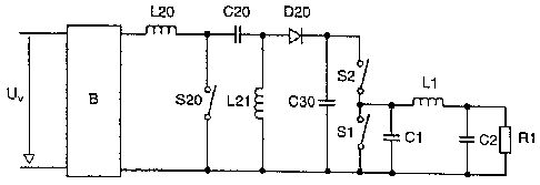
fig. 1 shows a highly schematic circuit diagram of a
ballast according to the invention as the first
exemplary embodiment.
fig. 2 shows real measurement curves relating to the
ballast shown in fig. 1.
fig. 3 shows a highly schematic circuit diagram of a
ballast according to the invention as the second
exemplary embodiment.
Detailed description of the invention
Fig. 1 shows a schematic illustration of a ballast
according to the invention containing two converters.
An SEPIC converter known to those skilled in the art
and described, for example, in DE 101 10 239.9 produces
an intermediate circuit voltage across a storage
capacitor C30, from which a half-bridge circuit having
two switching transistors S1 and S2 is supplied.
CA 02486782 2004-11-04
- 6 -
In the ballast shown in fig. 1, an AC supply voltage
Uv, generally a conventional domestic power supply
voltage, is rectified via a bridge rectifier B. There
is thus in fig. 1 a rectified, positive potential on
the line branch running horizontally at the top and a
rectified, negative potential, which generally
represents the reference potential, on the lower line
branch parallel thereto. The rectified AC voltage forms
the input of the SEPIC converter, which has the
inductors L20 and L21, the capacitor C20, the rectifier
diode D20 and the switching transistor S20 and is
driven by a drive circuit (not shown).
The capacitor C30 acts as a storage capacitor and needs
to be charged by the SEPIC converter from the rectified
AC voltage to a DC voltage which is as constant as
possible. In this case, the intention is for the power
consumption from the power supply system to follow the
sinusoidal characteristic of the system voltage in a
manner which is as interference-free as possible.
Owing to an alternating switching operation of the
switching transistor 520, the coil L20 in the switch-on
state is charged from the rectified system voltage to a
specific current and is discharged in the switch-off
state of the switching transistor S20 to the capacitor
C20. In the same way, the coil L21 is charged during
the switch-on times of the switching transistor S20 and
is discharged during the switch-off times to the
storage capacitor C20. In this case, the polarity of
the diode D20 is to be taken into account. There is so-
called noncontinuous operation if the switch-off times
of the switching transistor S20 are sufficiently long
for the current in the rectifier diode D20 to be
reduced to zero. In this case, on average the capacitor
C20 remains charged essentially to the value of the
instantaneously rectified supply voltage. This in turn
I
CA 02486782 2004-11-04
_ 7 _
results in the storage capacitor C30 being charged
during the switch-off times only with the induction
voltage produced by the coil L21. Owing to a
corresponding duty ratio, i.e. the ratio between the
switch-on times and switch-off times, and taking into
account the load R31, essentially any desired DC
voltage may be set across the capacitor C30 which may
in particular be smaller than the amplitude of the
system voltage. The SEPIC converter then functions as a
step-down converter. The capacitor C20 ensures to a
certain extent that the two inductors L20 and L21 are
decoupled from one another, with the result that, in
contrast to simple step-up converters such as the
step-up converter, the voltages produced by the coil
L20 do not add up to the instantaneous system voltage.
Connected in parallel with the lower one of the
switching transistors S1 and S2 is a trapezoidal
capacitor C1 which nevertheless also relieves the load
on the upper switching transistor S2 at the same time,
i.e. acts as a trapezoidal capacitor for both switching
transistors. L1 is the reference given to a
conventional lamp inductor, and C2 is the reference
given to a conventional resonance capacitor, as are
known from the circuitry for low-pressure discharge
lamps. The low-pressure discharge lamp itself is not
illustrated. It is represented by a resistor R1
connected in parallel with C2. If a discharge lamp is
provided as the load, a so-called coupling capacitor
must also be connected in series.
The switching transistors S1 and S2 are clocked by a
microcontroller (likewise not shown) which likewise
clocks the SEPIC converter.
In the event of a lamp failure, for example in the
event of an electrode breakage during operation or
following unsuccessful starting attempts, the
CA 021486782 2004-11-04
microcontroller continues to operate the SEPIC
converter according to the invention, and to be precise
at a power level which is as low as possible. This
power which is indispensable for the operation of the
SEPIC converter would continue to charge the storage
capacitor with the intermediate circuit voltage if it
is not dissipated. For this reason, the half-bridge
oscillator likewise continues to operate according to
the invention, but in an operating mode which is
different than for normal operation. This is
illustrated in fig. 2. Channel CH1 and channel CH2 each
show a drive signal of the upper half-bridge transistor
S2 and of the lower half-bridge transistor S1,
respectively. Channel CH3 shows the voltage across the
center tap of the half-bridge.
The switching transistors are supplied with the control
signals specified and are thus each alternately closed
for a certain amount of time in the region of the
extreme values of the voltage curve (illustrated at the
top of fig. 2) of the center tap of the half-bridge.
Whilst one of the switching transistors is closed, the
trapezoidal capacitor C1 is recharged, the energy from
the trapezoidal capacitor in this case primarily being
dissipated in the intrinsic resistance of the switching
transistor, i.e., for example, in its drain-source
resistance when it is switched on. The charge stored in
the capacitor is in this case almost completely reduced
by a sufficiently long switch-on time of the switching
transistor, i.e., for example, at ten times the
critical RC constant, with the result that the energy
stored in the capacitor is almost completely
dissipated. The total dissipated power is in this case
calculated as
Pv = f ~ C1 ~ U2
where
CA 02486782 2004-11-04
_ g -
Pv: Power loss
f: Switching frequency of the half-bridge in this
operating mode
C1: Capacitance of the trapezoidal capacitor
U: Voltage step across the trapezoidal capacitor C1.
In this example, it is shown in fig. 2 that the period
duration of the half-bridge operation corresponds to
six times the natural frequency of the remaining load
circuit, with the result that a switching operation
takes place at every sixth extreme point.
The invention thus provides an "emergency operating
form" of the ballast, which is possible without
additional components, having a PFC circuit (SEPIC
converter) which continues to operate and results in
power dissipation in the operating mode described of
the operated half-bridge. Auxiliary voltages and power
supplies derived from the SEPIC converter, for example
for the microcontroller, can thus continue to run, and
memory contents can be maintained. In particular, it is
thus possible to prevent the microcontroller from
"forgetting" that a lamp failure has taken place and
for this reason continuing to step up and make starting
attempts. If, however, the user turns the system switch
off and on again, the operating state described here is
also interrupted and a new starting attempt is begun.
The invention can be used in principle, for example,
also in the case of single-stage converter concepts in
which, for example, an auxiliary power supply could be
derived from a half-bridge topology. In this case, the
half-bridge itself could continue to operate in the
described "emergency operating state", in which the
microcontroller or another controller continues to be
supplied from the half-bridge itself.
A corresponding second exemplary embodiment is shown in
CA 02486782 2004-11-04
- 10 -
fig. 3. Here, corresponding reference numerals have
been used for circuit elements corresponding to the
first exemplary embodiment. The input voltage Ue
illustrated on the left-hand side could be supplied,
for example, by the bridge rectifier B shown in fig. 1
using additional filters, if necessary. Here, no
converter is in any case provided as the PFC circuit.
An auxiliary power supply from the recharge current in
the trapezoidal capacitor C1 is therefore built up
here. This takes place using the diodes Dl and D2, the
switch S3 and the backup capacitor C3. The switch S3 is
driven for this purpose by means of a two-step
controller and thus regulates the voltage across the
backup capacitor C3. A circuit 30 to be supplied with
power is connected to the backup capacitor C3 and draws
the necessary energy for its operation from C3.
Connected in parallel with C2 is an output voltage Uo,
to which a load, for example a discharge lamp or an
LED, can be connected.
When the lamp is switched off, i.e. when there is no
current flowing through L1, the half-bridge Sl, S2 can
be clocked in the manner already described for the
first exemplary embodiment, and the auxiliary voltage
supply can thus be maintained.
In this operating mode, the resonant circuit comprising
L1 and C2 is not excited.