Note: Descriptions are shown in the official language in which they were submitted.
CA 02486986 2004-11-22
DESCRIPTION
Compound Semiconductor Wafer and Manufacturing Method Thereof
Technical Field
The present invention relates to a compound semiconductor wafer for a near-
infrared sensor for food, medical or environmental inspection, as well as to a
method of
manufacturing the same.
Background Art
As a near-infrared sensor having sensitivity in the near-infrared wavelength
range
of 1.7 ~m to 2.6 p.m, one having such a structure has been known in that a p-
type
semiconductor layer is formed by diffusing zinc in an epitaxial wafer having
an InZGa,_
ZAs layer (hereinafter referred to as an InGaAs layer) with large lattice
constant as a
light receiving layer, and positive and negative electrodes are arranged on
upper and
lower surfaces thereof. Many substances surrounding us, including organic
substances,
water, gas and the like absorb waves having the wavelength in the near-
infrared range of
1.7 p.m to 2.6 pm, and therefore, such a sensor is expected to have wide
applications in
the field of environmental inspection, medical inspection, food analysis,
temperature
detection and the like.
In the near-infrared sensor described above, on an InP substrate, an InGaAs
light
receiving layer having a lattice constant larger than that of the InP
substrate is formed.
Therefore, the difference in lattice constant is adjusted by providing,
between the InP
substrate and the InGaAs light receiving layer, a plurality of step layers and
a buffer
layer formed thereon to be in contact with InGaAs layer. An epitaxial wafer
having a
lattice constant different from that of the substrate is referred to as a
lattice mismatch
type epitaxial wafer. The structure in which the step layers and a buffer
layer are
inserted between the substrate and the light receiving layer described above
has been
-1-
CA 02486986 2004-11-22
proposed repeatedly (for example, in Japanese Patent Laying-Open Nos. 2001-
156324,
2001-102620 and 06-216403), since it has been found that the InGaAs layer has
sensitivity in the near-infrared range.
Disclosure of the Invention
In a ternary compound semiconductor consisting of (group 3/group 3/group 5)
elements, a band gap is determined uniquely by its composition or by the
lattice constant
that is determined by the composition. Therefore, the ratio of elements of
InAsP
constituting each of the step layers and the buffer layer is varied to
gradually increase
the lattice constant as described above, so that the lattice constant is
varied from that of
InP substrate to a desired lattice constant of the InGaAs light receiving
layer.
As a method of growing a lattice mismatch type epitaxial wafer for the near-
infrared sensor, vapor deposition such as OMVPE (Organo Metallic Vapor Phase
Epitaxy) or VPE (Vapor Phase Epitaxy) has been known. Among these, VPE method
is known to have high growth rate.
However, even when the light receiving layer of InGaAs is formed with the step
layers provided to have gradually increasing lattice constant as described
above, it has
been difficult to stably manufacture an InGaAs layer having a satisfactory
crystal
characteristic. This results in large dark current, and therefore, though near-
infrared
sensors of low sensitivity could be obtained, stable, highly sensitive and low-
noise
products could not be obtained.
An object of the present invention is to provide a compound semiconductor
wafer and manufacturing method thereof that enable stable manufacture of an
InGaAs
light receiving layer having superior crystal characteristic.
The present invention provides a compound semiconductor wafer including an
InGaAs layer as a light receiving layer formed on an InP substrate. The wafer
includes
an InAsxP l.x step layer consisting of a plurality of layers (x differs layer
by layer) formed
in contact with and on the InP substrate, and an InAsyPl_Y buffer layer
positioned in
-2-
CA 02486986 2004-11-22
contact with and on the step layer, sandwiched between the InP substrate and
the
InGaAs layer. The plurality of step layers and the buffer layer have mutually
different
lattice constants that gradually become closer from that of the InP layer to
that of the
InGaAs layer. Further, the maximum value of PL light emission intensity at the
interface of each of the plurality of step layers and the buffer layer is, at
every interface,
smaller than 3/10 of the maximum PL light emission intensity of the buffer
layer.
The PL light emission intensity reflects crystal characteristic of the portion
that
emits light, and the PL light emission intensity becomes higher at a portion
having higher
crystal characteristic. In the structure described above, the crystal
characteristic at the
interface of the step layers and the buffer layer is deteriorated as edge
dislocations and
threading dislocations are concentrated, while the crystal characteristic in
the buffer
layer is three times or more higher than that of the interface, as indicated
by PL light
emission intensity. In such a stacked structure, misfit dislocations are not
transferred
from the interface to the upper layer. That the misfit dislocations are not
transferred to
the upper layer has been confirmed by the inventors of the present invention
by
inspection with TEM (Transmission Electron Microscopy). If the thickness of
the
upper layer is not larger than a prescribed thickness, good crystal
characteristic cannot
be expected because of the disorder at the interface as an underlying layer.
If the
thickness is large enough not to be influenced by the disorder of the
interface, however,
an epitaxial film having very high crystal characteristic can be obtained.
Typically, the
thickness of the buffer layer mentioned above is about twice that of each step
layer.
As to the maximum value of the PL light emission intensity, the PL light
emission intensity of a prescribed area of a wafer is measured. The measured
PL light
emission intensity is classified into about ten levels, and an average value
of the highest
level intensity is used as the maximum value.
According to another aspect, the present invention provides a compound
semiconductor wafer including an InGaAs layer as a light receiving layer
formed on an
InP substrate. The wafer includes an InAsXPI_X step layer consisting of a
plurality of
-3-
CA 02486986 2004-11-22
layers formed in contact with and on the InP substrate, and an InAsyPl_y
buffer layer
positioned in contact with and on the step layer, sandwiched between the InP
substrate
and the InGaAs layer. The plurality of step layers and the buffer layer have
mutually
different lattice constants that gradually become closer from that of the InP
layer to that
of the InGaAs layer. Further, the maximum value of PL light emission intensity
of the
step layers is, in every layer, not larger than 7110 of the maximum PL light
emission
intensity of the buffer layer.
This structure is assembled in view of crystal characteristic inside the step
layers
and the buffer layer. The ratio between the PL light emission intensity inside
the step
layers to that inside the buffer layer becomes smaller than in a conventional
example.
This means that the buffer layer farther from the InP substrate has better
crystal
characteristic than the step layers that are thinner and closer to the InP
substrate.
According to a further aspect, the present invention provides a compound
semiconductor wafer including an InGaAs layer as a light receiving layer
formed on an
InP substrate. The wafer includes an InAsXP 1_X step layer consisting of a
plurality of
layers formed in contact with and on the InP substrate, and an InAsyPl_y
buffer layer
positioned in contact with and on the step layer, sandwiched between the InP
substrate
and the InGaAs layer. The plurality of step layers and the buffer layer have
mutually
different lattice constants that gradually become closer from that of the InP
layer to that
of the InGaAs layer. The maximum PL light emission intensity of at least the
first step
layer that is in contact with the InP substrate among the plurality of step
layers is smaller
then 1/10 of the maximum PL light emission intensity of the buffer layer.
In the above described structure, defects are concentrated in a layer or
layers
close to the InP substrate such as the first step layer that is in contact
with the InP
substrate, both inside the layer and at the interface. Therefore, distortion
is released at
least in the first step layer, and not propagated to an upper layer. As a
result, an
epitaxial film having superior crystal characteristic can be formed at the
buffer layer or
light receiving layer as the upper layer, whereby dark current resulting from
crystal
CA 02486986 2004-11-22
defects can be suppressed and a highly sensitive near-infrared sensor can be
obtained.
The PL light emission intensity of the second step layer positioned on and in
contact with the first step layer may also be smaller than 1/10 of the peak PL
light
emission of the buffer layer.
According to a still further aspect, the present invention provides a compound
semiconductor wafer including an InZGai-ZAs layer as a light receiving layer
formed on
an InP substrate. The wafer includes an InAsXPI_X step layer consisting of a
plurality of
layers formed in contact with and on the InP substrate, and an InAsyPl_y
buffer layer
positioned in contact with and on the step layer, sandwiched between the InP
substrate
and the InZGaI_ZAs layer. The plurality of step layers and the buffer layer
have mutually
different lattice constants that gradually become closer from that of the InP
layer to that
of the InZGaI_ZAs layer. The peak composition ratio of As andlor P of at least
one
interface between each of the plurality of step layers and the buffer layer is
closer to the
corresponding composition ratio of the InP substrate than the corresponding
composition ratio of the step layer that is in contact with the interface of
interest on the
side of the InP substrate and that of the step layer that is in contact with
the step layer
on the side of the InP substrate.
In this structure, the step layers are formed with compositions adjusted so as
to
attain matching lattice constant from the InP substrate to the buffer layer,
while the
compositions at the interfaces are reverse to such adjustment. As the
composition is in
one-to-one correspondence with the lattice constant, it follows that the
lattice constants
at the interface are adverse to each other, resulting in misfit dislocation
concentration at
the interface. When the misfit dislocations axe concentrated at the interface,
misfit
dislocations in the step layers and in the buffer layer decrease, and
therefore, a light
receiving layer having superior crystal characteristic can be obtained.
The present invention provides a method of manufacturing a compound
semiconductor wafer that includes an InGaAs layer as a light receiving layer
formed on
an InP substrate, an InAsXPI_X step layer consisting of a plurality of layers
formed in
-5-
CA 02486986 2004-11-22
contact with and on the InP substrate, and an InAsyPl.y buffer layer
positioned in contact
with and on the step layer, sandwiched between the InP substrate and the
InGaAs layer.
The plurality of step layers and the buffer layer have mutually different
lattice constants
that gradually become closer from that of the InP layer to that of the InGaAs
layer. In
manufacturing such a compound semiconductor wafer, growth is interrupted every
time
each of the plurality of step layers and the buffer layer is formed.
As the growth is interrupted as described above, steepness in composition
variation that vary layer by layer among the step layers and the buffer layer
can be made
higher. The steep transition of compositions at the interface of each layer
also
increases steepness in lattice constant variation, and therefore, it acts to
suppress
extension or propagation of defects described above.
Here, growth interruption refers to a state in which growth is stopped for a
prescribed time period, for example one minute or longer, and the wafer is
held in that
state. Specifically, the growth is stopped by stopping supply of the material
gas to the
substrate for growth for a prescribed time period, the material gas to be
supplied to the
substrate is adjusted to surely have a prescribed composition during that
period, and the
supply of the material gas to the substrate is resumed. By such growth
interruption, an
interface can be obtained at which composition and lattice constant vary
steeply.
The foregoing and other objects, features, aspects and advantages of the
present
invention will become more apparent from the following detailed description of
the
present invention when taken in conjunction with the accompanying drawings.
Brief Description of the Drawings
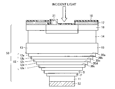
Fig. 1 represents a near-infrared sensor incorporating a compound
semiconductor wafer in accordance with the present invention.
Fig. 2 represents a film forming apparatus used for manufacturing a compound
semiconductor wafer in accordance with an embodiment of the present invention.
Fig. 3 is a transmission electron microscopic photograph showing a cross
section
-6-
CA 02486986 2004-11-22
of a compound semiconductor wafer (Sample 1) in accordance with the present
invention.
Fig. 4 is a transmission electron microscopic photograph showing a portion
near
the step layer of Sample 1.
Fig. 5 is a transmission electron microscopic photograph showing a portion
near
the light receiving layer of Sample 1.
Fig. 6 is a transmission electron microscopic photograph showing a portion
near
the step layer of a comparative example (Sample 2).
Fig. 7 is a transmission electron microscopic photograph showing a portion
near
the light receiving layer of Sample 2.
Fig. 8 shows PL light emission intensity distribution of the compound
semiconductor wafer in accordance with the present invention (Sample 1).
Fig. 9 shows PL light emission intensity distribution of the compound
semiconductor wafer of the comparative example (Sample 2).
Fig. 10 three-dimensionally shows PL light emission intensity distribution of
the
compound semiconductor wafer in accordance with the present invention.
Fig. 11 represents relation between PL light emission intensity ratio and
contrast
number resulting from distortion in the step layer.
Fig. 12 represents relation between the PL light emission wavelength of light
receiving layer and buffer layer of the compound semiconductor wafer,
specifying the
range in which the light receiving layer has superior crystal characteristic.
Fig. 13 shows a result of SIMS analysis of Sample 1 in accordance with the
present invention.
Fig. 14 shows a result of SIMS analysis of Sample 2 of the comparative
example.
Best Modes for Carrying Out the Invention
In the following, an embodiment of the present invention will be described
with
reference to the figures. Fig. 1 is a cross sectional view showing a near-
infrared sensor
CA 02486986 2004-11-22
using a compound semiconductor wafer in accordance with the present invention.
In
compound semiconductor wafer 50, on an InP substrate 11, a step layer 12 of
InAsP is
formed, and a buffer layer 13 of InAso.6Po.a is further arranged thereon. Step
layer 12
and buffer layer 13 are arranged to make smooth the difference in lattice
constant
between a light receiving layer 14 of Ino,g2GaousAs and the InP substrate.
Step layer 12 includes a number of layers, and composition of each layer is
selected such that a layer closer to the light receiving layer comes to have
larger lattice
constant. In Fig. 1, the layers are denoted by 12a, 12b, 12c, ... from the one
closer to
buffer layer 13 toward the InP substrate. Further, the step layer that is
positioned on
and in contact with the InP substrate is denoted as a first step layer F, and
a second step
layer S is arranged on and in contact with the first step layer. In the
embodiment of the
present invention, what is important is whether PL light emission occurs in
the first step
layer F and the second step layer S. Further, in the compound semiconductor
wafer of
the present embodiment, what is important is the interface of the step layers
and the
buffer layer. As shown in Fig. 1, these interfaces are denoted by 30a, 30b,
30c, ...
from the buffer layer toward the InP substrate.
PL light emission occurs when portions of compound semiconductor wafer 50 is
irradiated with light. In the present embodiment, the maximum value of PL
light
emission intensity at the interface of each of the plurality of step layers
and the buffer
layer is, at every interface, smaller than 3/10 of the peak intensity of PL
light emission of
the buffer layer.
As a modification, the maximum value of PL light emission intensity of the
plurality of step layers may be not higher than 7/10 of the maximum value of
PL light
emission of the buffer layer.
Further, as another modification, the maximum value of PL light emission
intensity of at least the first step layer positioned on and in contact with
the InP
substrate among the plurality of step layers is smaller than 1/10 of the peak
intensity of
PL light emission of the buffer layer. In this case, the maximum value of PL
light
_g_
CA 02486986 2004-11-22
emission intensity of the second step layer positioned on and in contact with
the first
step layer may be smaller than 1/10 of the peak intensity of PL light emission
of the
buffer layer.
In order to use compound semiconductor wafer 50 described above as a near-
infrared sensor, first, a Zn diffusion mask is arranged on a window layer 16.
Thereafter,
an n-type electrode 22 is formed to be in ohmic contact with a rear surface of
InP
substrate 11, and a p-type electrode 21 is formed to be in ohmic contact with
window
layer 16. Thereafter, an anti-reflection film 18 is formed thereon for
coverage.
Near-infrared incident light passes through window layer 16, and excites
electrons in the valence band in light receiving layer 14. Consequently, a
current flows
between p-type electrode 21 and n-type electrode 22, to attain the fiznction
of a near-
infrared sensor.
Fig. 2 shows a method of manufacturing the compound semiconductor wafer in
accordance with the present invention. The apparatus shown in Fig. 2 is a
chloride
vapor deposition apparatus. According to the chloride method, hydrogen is used
as a
carrier gas, and when an InGaAs film is to be formed, AsCl3 is introduced to
the
apparatus. In the apparatus, AsCl3 and HZ are thermally decomposed to As4 and
HCI.
HCI separately reacts to Ga and~In, generating GaCI and InCI, whereby an
InGaAs film
can be formed on the substrate. When the composition is to be varied, the
amount of
AsCl3 to be reacted with Ga or the amount of AsCl3 to be reacted with In is
changed.
When an InAsP film is to be formed, hydrogen gas is used as a carrier gas as
in the case
described above, and separate reactions to AsCl3 and PCI3 are induced, so that
an InAsP
film is formed on the substrate. Compositions of As and P of the InAsP film
are
controlled by adjusting the amount of supplied material gas.
In the chloride method, the growth rate is as high as S times that of the
conventionally used OMVPE (Organic Metal Vapor Plasma Enhanced) method.
Therefore, it is advantageous in forming a thick layer, and a film having good
crystal
characteristic can be obtained.
-9-
CA 02486986 2004-11-22
The apparatus shown in Fig. 2 has the following characteristics.
( 1 ) A film forming space for the InAsP film is separated from-a film forming
space for the InGaAs film, by a screen-type partition.
(2) At the time of film formation, it is possible to independently form a film
or to
interrupt growth, with the substrate arranged in either one of the film
forming spaces.
Particularly, it is possible to form the step layer of a prescribed
composition and
thereafter to interrupt growth. At this time, the substrate, on which the film
has just
been formed, may be covered by a protection plate to quickly shield from the
material
gas. Therefore, the time period in which the substrate is exposed to the
material gas of
which composition is being varied can be eliminated.
Next, when a step layer of a different composition is to be formed, after the
adjustment of material gas composition is finished and prescribed desired
composition is
attained, the protection plate may be removed and the material gas as such can
be
supplied to the substrate.
Consequently, the steepness in composition variation at the interface can be
improved, and therefore, steepness in the lattice constant variation can also
be improved.
As a result, misfit dislocations and the like can be concentrated at the
interface, so that
extension or propagation of dislocations and the like to an adjacent layer can
be
prevented. Thus, a light receiving layer having superior crystal
characteristic can be
obtained.
(Examples)
Using the chloride VPE apparatus shown in Fig. 2, compound semiconductor
wafer 50 shown in Fig. 1 was manufactured. The object wavelength of the light
to be
received by the light receiving layer, that is, the PL light emission
wavelength was, by
way of example, 2200 nm. The PL light emission wavelength of the buffer layer
will be
indicated in Fig. 11, which will be described later. Further, an n-type
impurity is
introduced to be lE+18 or higher, in the InAsxPl_X step layer 12 and in
InAs3,P1_y buffer
layer 13.
- 10-
CA 02486986 2004-11-22
As to the manufacturing method, when the step layers and the buffer layer are
formed, growth is interrupted every time a layer is formed, so as to improve
steepness of
composition and lattice constant variation, as already described with
reference to Fig. 2.
Fig. 3 is a transmission electron microscopic photograph showing a cross
section
of Sample 1 of the compound semiconductor in accordance with the present
invention.
On InP substrate 11, first step layer S and second step layer F are formed,
and five step
layers 12e to 12a are formed thereon. On these step layers, buffer layer 13 is
formed,
and light receiving layer 14 and window layer 16 are further provided.
In Sample 1 of the present invention, PL light emission intensity of InGaAs
light
receiving layer 14 is very high, as will be described later. Referring to Fig.
3,
brightness/darkness contrast resulting from a distortion is clearly recognized
at each
interface of InAsXPi_X step layers. Such brightness/darkness contrast
resulting from a
distortion, however, is not recognized at the interface between InAsyPl_y
buffer layer 13
and InGaAs light receiving layer 14 or at the interface between InAsP window
layer 16
and InGaAs light receiving layer 14.
Fig. 4 is a transmission electron microscopic photograph showing, in
enlargement, the step layers of Sample 1 in accordance with the present
invention. In
Fig. 4, it can be recognized that contrast 36 representing high density
dislocations is
formed at the interface of each step layer and extended into the step layers.
On the
contrary, in Fig. 5, the contrast at the interface between each of InGaAs
light receiving
layer 14 and adjacent InAs},P,_y buffer layer 13 and InAsP window layer 16 is
not clear,
indicating that the density of dislocations is low.
Fig. 6 is a transmission electron microscopic photograph showing a cross
section
of a compound semiconductor wafer of Sample 2, which was grown without growth
interruption, not considering steepness of composition variation at the
interface between
each of the step layers. Referring to Fig. 6, extension of dislocations from
each
interface of the step layers is not recognized, and the brightness/darkness
contrast
resulting from dislocation density is low. The magnification of Fig. 6 is
approximately
-11-
CA 02486986 2004-11-22
the same as that of Fig. 3, and therefore, by the comparison between Figs. 3
and 6,
sharper contrast at each interface of the step layers in Fig. 3 can be
recognized. It is
noted, however, that brightness/darkness contrast 31 resulting from distortion
is
recognized in InAsyPl_y buffer layer 13.
Referring to Fig. 7, brightnessldarkness contrast 32 is recognized in InGaAs
light
receiving layer 14, and brightness/darkness contrast 33 is also recognized in
InAsP layer
16. Further, the contrast representing the dislocation density at the
interface of
InAsyP~_y buffer layer 13 and of InAsP window layer 16 is higher than that of
Fig. 5.
Specifically, it is observed in Sample 1 of the compound semiconductor wafer
in
accordance with the present invention, that the dislocation density at each
interface of
the step layers is higher than Sample 2, the dislocations are extended into
each step layer,
and that the dislocation density is lower at the interface of the buffer layer
or the
window layer adjacent to light receiving layer 14.
The PL light emission intensity distribution on the cross section of Sample 1
of
the compound semiconductor wafer in accordance with the present invention was
measured. Fig. 8 shows the measurement result. In Fig. 8, the abscissa
represents
wavelength (nm) of PL light emission, and the ordinate represents length (nm}
or
distance from a reference position. Therefore, thickness of each layer can be
known
from the ordinate. The intensity of PL light emission is generally represented
by colors
in actual data. The intensity distribution, however, can be understood by
black-and-
white representation with the intensity level indicated by numerical values,
as in Fig. 8.
In Fig. 8, the highest intensity of PL light emission corresponds to unit 8,
and
unit 8 is divided into 10 levels, as shown in the figure with corresponding
numerical
values. The unit of "unit 8" mentioned above is particular to the measurement
apparatus. Fig. 8 shows the wavelength range covering the emission wavelength
of
InP substrate 11 to the emission wavelength of buffer layer 13 . Specifically,
the range
of 2200 nm, that is the wavelength of light receiving layer 13, is not
covered. The
reason is as follows. In order to measure the wavelength of 2200 nrn, a near-
infrared
-12-
CA 02486986 2004-11-22
sensor using a compound semiconductor wafer, that is the object of the present
invention, must be used, and such a range cannot be measured unless the sensor
is
switched to a special sensor.
From Fig. 8, the following can be understood.
(al) PL light emission is not observed at the first step layer F and the
second
step layer S. The maximum value of PL light emission intensity of the buffer
layer is
represented by level 10, while the intensity of first step layer F and second
step layer S is,
to say the least, not high enough to reach level 1. Therefore, the light
emission
intensity is at most smaller than level 1.
(a2) At the interface between two step layers 12b and 12c and at the interface
between two step layers 12d and 12e, the maximum value at the interface, that
is, level 2,
is attained. The crystal characteristic at the interface is as small as 2110,
as compared
with level 10 corresponding to the maximum PL light emission intensity of the
buffer
layer.
(a3) The PL light emission intensity within the step layers is level 3 at the
highest,
that is, 3l10 of the highest value of buffer layer 13.
As a comparative example, the PL light emission intensity distribution of
Sample
2 was measured, which sample of the compound semiconductor wafer was formed
using
the chloride VPE apparatus shown in Fig. 2, with the step layers and the
buffer layer
formed without growth interruption. The result of measurement is as shown in
Fig. 9.
In the representation given in Fig. 9, 90 % of the highest intensity is
regarded as unit 3.5..
Namely, the highest intensity corresponds to unit 3.89 (3.5 unitl0.9). As to
the unit,
the PL light emission intensity in the step layer is level 3 at the highest as
described
above, which is smaller than that of buffer layer 13. In Fig. 9, the highest
intensity of
3.89 is classified into 10 levels, as shown in the figure with corresponding
numerical
values. It may be considered that the sensitivity of measurement is improved
in Fig. 9
than in Fig. 8. From the comparison of Fig. 9 with the example of the present
invention shown in Fig. 8, the following can be understood.
-13-
CA 02486986 2004-11-22
(bl) PL light emission is recognized even in the first step layer F and the
second
step layer S. Considering the absolute value of PL light emission intensity,
this result
may be derived from higher sensitivity. When compared with the highest
intensity of
the buffer layer, however, the intensity of first step layer F is level 2 and
that of the
second step layer is level 7, and thus, the ratio to the highest intensity of
the buffer layer
is 2/10 and 7/10, respectively. Such intensity ratio is considerably different
from the
value of the present invention, which is smaller than 1110.
(b2) Referring to Fig. 9, the highest value of PL light emission at the
interface is
level 4. Namely, the ratio to the highest value of the buffer layer is 4110.
This is
significantly higher than the ratio 2/10 of the present invention.
(b3) The highest PL light emission intensity inside the step layers is level
10 of
step 12e, which is the same as the highest level of buffer layer 13. The ratio
is 10!10,
that is, 1. This is a big difference between the example of the present
invention and the
comparative example.
As to the PL light emission intensity of the light receiving layer, which is
the
most important, is given by the ratio to the comparative example, in
accordance with the
following equation.
(maximum intensity of PL light emission intensity of light receiving layer 14
of
the wafer shown in Fig. 8)/(maximum intensity of PL light emission intensity
of light
receiving layer of the wafer shown in Fig. 9) = 16/l.
From the foregoing, it follows that light receiving layerl4 of the compound
semiconductor wafer in accordance with the present invention has 16 times
higher light
receiving sensitivity than the light receiving layer of the comparative
example. It is not
simply the case that the defect density of the example in accordance with the
present
invention is reduced to 1/16 that of the comparative example. It is noted,
however,
that the defect density in the light receiving layer of the present invention
is remarkably
reduced from that of the comparative example, and the light receiving layer
having
superior crystal characteristic is obtained. As a result, dark current can be
reduced
-14-
CA 02486986 2004-11-22
significantly, and the sensitivity in the near-infrared range can remarkably
be improved.
Fig. 10 represents the PL light emission intensity in a three-dimensional
manner,
with the PL light emission intensity of the example in accordance with the
present
invention shown in Fig. 8 plotted along the vertical axis. The maximum PL
light
emission intensity in the step layer is about 40 % of the maximum PL light
emission
intensity of the buffer layer, matching the representation of Fig. 8.
Fig. 11 represents contrast number resulting from distortion in the InAsxP~_X
step
layer in a prescribed range on the abscissa, and represents PL light emission
intensity
ratio of InGaAs light receiving layer 14 on the ordinate, plotted for Samples
1 to 3.
Sample 2 is a compound semiconductor wafer not belonging to the present
invention,
which is almost free of any growth interruption and in which steepness in
composition
variation is not so strictly managed as in Sample 1.
Referring to Fig. 11, the contrast number resulting from distortion in the
step
layer is in proportion to the PL light emission intensity in the light
receiving layer, and it
can be understood that the larger the contrast number resulting from
distortion in the
step layer, the higher the PL light emission intensity in the light receiving
layer. This
relation well matches the mechanism described above, that is, misfit
dislocations in
layers lower than the light receiving layer are not transferred or extended to
the light
receiving layer but locally held at the interfaces and inside the step layers,
so that crystal
characteristic of the light receiving layer is improved and the PL light
emission intensity
is improved.
Fig. 12 represents relation between the PL light emission wavelength 7~s of
InGaAs light receiving layer 14 and PL light emission wavelength ~,b of InAsP
buffer
layer 13, specifying the range in which the light receiving layer has high PL
light
emission intensity. The examples described above are also plotted as points
within this
range. This range can be represented as ~,s - 800 nm _< ~,b <_ ~,s - 620 nm.
When this
relation is satisfied, it is considered that misfit dislocation is not likely
between a lattice
of the InGaAs light receiving layer and the lattices of InAsP buffer layer as
well as
-15-
CA 02486986 2004-11-22
InAsP window layer.
When a compound semiconductor wafer is actually manufactured, the wafer that
satisfies the range shown in Fig. 12 can be manufactured through the following
steps.
(sl) First, the wavelength of light to be received by light receiving layer 14
is
determined. This is none other than determination of wavelength as the object
of the
sensor. Further, it is the same as determination of the PL light emission
wavelength.
Determination of PL light emission wavelength is equivalent to determination
of band
gap, and therefore, composition and lattice constant are also determined
naturally.
(s2) PL light emission wavelength of buffer layer 13 is determined based on
Fig.
12. This is the same as determination of PL light emission wavelength of
window layer
16. Therefore, composition and lattice constant of the buffer layer and of the
window
layer are determined.
(s3) From the lattice constant of the buffer layer determined in (s2) and from
the
lattice constant of InP substrate, the number of step layers to be inserted
and lattice
constants thereof are designed. The design of lattice constants also involves
composition design.
Through the steps (sl) to (s3) described above, the relation of PL light
emission
intensity of the light receiving layer and the buffer layer shown in Fig. 12
can be satisfied.
As a result, a light receiving layer having superior crystal characteristic
can be obtained,
and a highly sensitive near-infrared sensor with small dark current can be
obtained.
The result of SIMS (Secondary Ion Mass Spectroscopy) on cross sections of
Sample 1 (present invention) and Sample 2 (comparative example) will be
described in
the following. SIMS enables mass spectrometry of a small portion, and
therefore, mass
spectroscopy of the interface at each step layer, which is important in the
embodiment of
the present invention, is possible. Fig. 13 is a chart representing the result
of SIMS
analysis of Sample 1 (present invention). Referring to Fig. 13, it can be seen
that step
layer 12 includes step layers 12a, 12b, 12c, 12d with compositions of
InAsXPI_X varied
layer by layer. Specifically, the composition ratio of P in InAsXPI_X
decreases from InP
-16-
CA 02486986 2004-11-22
substrate 11 to buffer layer 13, while the composition ratio of As in InAsxP
l.X increases
from InP substrate 11 to buffer layer 13. This is to adjust the lattice
constant gradually
from InP substrate 11 to buffer layer 13.
At the interfaces 30a, 30b, 30c, 30d and the like of these step layers, P and
As
composition ratios represent variations that are adverse to the composition
variation
described above. Specifically, the peak composition ratio of As and P at the
interface
of a step layer is closer to the composition ratio of the InP substrate than
the
composition ratio of As and P of a preceding step layer, that is, the step
layer closer by
one to the InP substrate. At the interface, the composition does not become
closer to
the composition of the buffer layer but rather it has the reverse tendency.
Fig. 14 is a chart representing the result of SIM5 analysis of Sample 2
(comparative example). From this result, it can be seen that though the
composition
ratio of As and P vary at the interface of a step layer, there is no interface
of which
composition ratio peak value is closer to that of the InP substrate than that
of a
preceding step layer.
It can be concluded from the comparison between Figs. 13 and 14, that the peak
of composition ratio of As and P at the interface of a step layer is closer to
the
composition ratio of the InP substrate to the extent as described above,
because of the
fi~nction of growth interruption. The variation of composition ratio at the
interface
results from the interruption of growth that caused steep composition
variation between
each of the layers, and it involves concentration of misfit dislocations.
Specifically, the lattice constant and the composition ratio are in one-to-one
correspondence, and therefore, adverse variation in composition ratio at the
interface
mentioned above also means adverse variation in lattice constant, establishing
concentration of misfit dislocations. When the misfit dislocations are
concentrated to a
higher degree at the interface, the number of misfit dislocations decreases in
the step
layers and in the buffer layer, facilitating formation of a light emitting
layer having
superior crystal characteristic.
- 17-
CA 02486986 2004-11-22
(Additional Comments on the Embodiment)
1. In the present embodiment, wafer examples that satisfy all of the following
conditions (cl) to (c3) have been described.
(cl) Wafers in which maximum PL light emission intensity at the interface of
each of the plurality of step layers and the buffer layer is, at every
interface, smaller than
3/10 of the maximum PL light emission intensity of the buffer layer.
(c2) Wafers in which the maximum PL light emission intensity of the plurality
of
step layers is not larger than 7110 of the maximum PL light emission intensity
of the
buffer layer.
(c3 ) Wafers in which the maximum PL light emission intensity of at least the
first
step layer positioned on and in contact with the InP substrate among the
plurality of step
layers is smaller than 1/10 of the maximum PL light emission intensity of the
buffer layer.
It is noted, however, that the wafer of the present invention, in its broadest
scope, have only to satisfy one of the conditions (cl) to (c3).
2. In the present embodiment, when the growth is to be interrupted, supply of
the material gas is stopped by using a protection plate, to increase steepness
at the
interface. The method of interrupting growth is not limited to this method,
and any
method may be used provided that the material gas of different compositions
can be
supplied to the substrate for forming different step layers.
Modifications of the embodiment of the present invention will be briefly
described, also with reference to features already described in the embodiment
above.
In every compound semiconductor wafer in which PL light emission intensity of
the buffer layer is defined to be higher by a prescribed value or more than
the PL light
emission intensity of other portions, the lattice constant of the buffer layer
and the lattice
constant of the light receiving layer may be determined such that the PL light
enussion
wavelength ~.b of the buffer layer and the PL light emission wavelength ~,s of
the light
receiving layer satisfy the relation of ~,s - 800 nm <_ ~,b <_ ~,s - 620 nm.
When the relation of PL light emission intensity described above is satisfied
- 18-
CA 02486986 2004-11-22
between an underlying layer and the light receiving layer farmed on the
underlying layer,
the relation of lattice constants between the underlying layer and the light
receiving layer
is determined uniquely from the relation of PL light emission wavelength. By
selecting
the compositions of the buffer layer and of the light receiving layer to
satisfy the relation
of lattice constants that realizes the relation of PL light emission
wavelength described
above, and by stacking such layers, a light receiving layer having superior
crystal
characteristic can be obtained. The reason, however, is not known.
In order to have the PL light emission wavelengths of the buffer layer and of
the
light receiving layer satisfy the relation described above, the step layers
and the buffer
layer must have such composition sequences that enables the relation described
above.
The PL light emission wavelength of the light receiving layer described above
may be 1700 nm or longer. By selecting the composition to attain the desired
wavelength, a near-infrared sensor can be obtained.
In every compound semiconductor wafer in which the peak value of composition
ratio of As and/or P at the interface is defined, at the interface between the
buffer layer
and the step layer, the peak value of composition ratio of As and/or P may be
made
closer to the corresponding composition ratio of the InP substrate than that
of a step
layer that is in contact with the interFace on the InP substrate side and that
of a step
layer that is in contact with the step layer on the InP substrate side.
Further, both at the interface between the buffer layer and the step layer and
at
the interface between step layers closer to that interface, the peak value of
composition
ratio of As andlor P may be made closer to the corresponding composition ratio
of the
InP substrate than that of a step layer that is in contact with the interface
on the InP
substrate side and that of a step layer that is in contact with the step layer
on the InP
substrate side. Further, at all three of the interface between the buffer
layer and the
step layer, the interface between step layers closest to that interface and
the interface
between step layers second closest to that interface, the peak value of
composition ratio
of As and/or P may he made closer to the corresponding composition ratio of
the InP
-19-
CA 02486986 2004-11-22
substrate than that of a step layer that is in contact with the interface on
the InP
substrate side and that of a step layer that is in contact with the step layer
on the InP
substrate side.
As described above, as misfit dislocations are concentrated at interfaces
closer to
the buffer layer, crystal characteristic of the buffer layer and the light
receiving layer can
be improved.
In every compound semiconductor wafer in which PL light emission intensity of
the buffer layer is defined to be higher by a prescribed value or more than
the PL light
emission intensity of other portions, and in every compound semiconductor
wafer in
which the peak value of composition ratio of As andlor P at the interface is
defined, an
n-type impurity of at least lE + 18 may be introduced to the InAsXPI_X step
layer
consisting of the plurality of layers described above and to the
InAs~,PI_ybuffer layer.
Introduction of the impurity suppresses extension and propagation of defects
to adjacent
layers.
When the InAsXPI_x step layer including the plurality of layers and the
InAsyPl_Y
buffer layer are formed, growth may be interrupted every time a layer is
formed.
By the growth interruption mentioned above, the steepness of layer-by-layer
composition change can be improved. As a result, steepness in lattice constant
variation can also be improved. When the steepness in lattice constant
variation
becomes higher at an interface, it follows that the lattice constant varies
stepwise from
one layer to the other layer. In such a case, misfit dislocations generated at
a lower
layer are blocked at the portion where the lattice constant varies stepwise,
and prevented
from extending and propagating to the upper layer.
Therefore, different from an example in which growth is not interrupted and
the
composition varies continuously, the defect density is not released at the
interface as the
underlying layer. However, an epitaxial film free of defect extension or
propagation
from the underlying layer to the InGaAs light receiving layer can be obtained.
As a
result, an epitaxial layer having superior crystal characteristic can be
obtained when the
-20-
CA 02486986 2004-11-22
film has at least a prescribed thickness.
On a rear surface of the InP substrate opposite to the front surface on which
the
above-described light receiving layer is formed, similar layers as those on
the front
surface may be formed. This structure prevents warp of the wafer.
In the method of manufacturing the compound semiconductor wafer in
accordance with the present invention, when the InAsXPI_X step layer and the
InAsyPl_y
buffer layer are formed, such a film forming apparatus may be used that has a
film
forming space in which the material gas is directed to the substrate for
manufacturing
and a saving space to which the substrate is retreated from the film forming
space, and
when the growth is to be interrupted, the compound semiconductor wafer that is
being
manufactured may be retreated from the film forming space to the saving space.
According to this method, steepness in composition variation can be improved
when a film is to be formed with its composition varied from that of the
preceding layer.
Further, steepness in lattice constant variation can also be improved, and
propagation or
extension of defects including misfit dislocations to an upper layer can be
suppressed.
Further, when the InAsxPl_X step layer and the InAsyP,_y buffer layer are
formed,
a growing apparatus having two growth chambers may be used, and when the
growth is
to be interrupted in each chamber, a protection plate may be placed so that
material gas
supply to the substrate is stopped.
According to this method, the material gas can be supplied and stopped
instantly,
and steepness in composition variation at the interface can easily be
established.
Although the present invention has been described and illustrated in detail,
it is
clearly understood that the same is by way of illustration and example only
and is not to
be taken by way of limitation, the spirit and scope of the present invention
being limited
only by the terms of the appended claims.
Industrial Applicability
By the compound semiconductor wafer and manufacturing method thereof in
-21 -
CA 02486986 2004-11-22
accordance with the present invention, an InGaAs light receiving layer having
superior
crystal characteristic formed on an InP substrate can be obtained; and hence a
highly
sensitive near-infrared sensor with small dark current can be obtained. Thus
wide
applications mainly for near-infrared sensor are expected.
-22-