Note: Descriptions are shown in the official language in which they were submitted.
~y,~
Ref: 2154US Exp~ : Mail No. EV 224559789 US
.~
METHOD AND APPARATUS FOR ABERROSCOPE CALIBRATION AND
DISGRETE COMPENSATION
s TECHNICAL FIELD OF THE INVENTION
The present invention relates to optical measurement and correction
systems and methods, and, more particularly, to corneal topography and ocular
aberrations measurement and correction systems and methods.
BACKGROUND OF THE INVENTION
Wavefront measurement systems are known in the art for measuring and
modeling ocular aberrations, such as those taught by the assignee of the
present
~s invention (e.g., U.S. Pat. No. 6,271,914, the disclosure of which is
incorporated
hereinto by reference). This system and method uses Zernike polynomials to
reconstruct an aberrated wavefront reflected from an eye and to calculate a
desired profile for directing laser sculpting of the corneal surface. An
exemplary
schematic for such a wavefront measurement device is given in FIGURE 2 in
zo the '914 patent.
Although a number of aberroscope designs are known in the art,
calibration systems and methods are inadequate, as stated by the Opfical
Society of America Taskforce on Vision Science and Its Applications (USIA-2000
Zs and VSIA-2001 ). Calibration of wavefront analyzers is now typically
performed
at manufacturing sites, and not in the field. Further; classical tenses have
primarily been used to provide a known amount of defocus by moving the lens
back and forth in the optical path. This method has the disadvar~taages of
being
-1-
CA 02487018 2004-11-08
Ref: 2154US Expr ,, : Mail No. EV 224559789 US
useful for limited aberration types (defocus, spherical aberration, and coma)
and
having a high level of uncertainty.
Holographic optical elements are known in the art that can function as
s lenses. Among their advantages are that they are lightweight and relatively
inexpensive, can generate unique optical functions not possible with
conventional optical elements, and can be fabricated in a wide range of
materials.
Thus there is a need for a standard device that could be mass produced
for calibrating and validating aberrometers.
_2_
CA 02487018 2004-11-08
~
~ ,
Ref: 2154US . Exp~ . : Mail No. EV 224559789 US
BRIEF SUMMARY OF THE INVENTION
The embodiments of the present invention provide a device, system, and
s method for calibrating an aberroscope, such as, but not intended to be
limited
to, wavefront measurement devices for use in objective measurement of optical
aberrations. The present invention also encompasses a method for making such
a device and system.
An embodiment of the aberroscope calibration device of this invention
comprises an optical element that is insertable into an optical path of a
wavefront
analyzer. The optical element is adapted to induce a predetermined aberration
in a wavefront for presentation to the wavefront analyzer. Since the form of
the
aberration is known, the wavefront analyzer can be calibrated by comparing the
~s predetermined aberration with an aberration calculated by the wavefront
analyzer.
In specific embodiments, the optical element rnay comprise a lens
optimized for a specific power and aberration; a computer-generated hologram,
Zo such as a diffractive optical element; or a spatial light modulator. The
optical
element may be transmissive or reflective.
A system for calibrating an aberroscope in accordance with this invention
can comprise an optical element and a wavefront analyzer, the wavefront
zs analyzer further comprising a wavefront detector. The wavefront detector is
-3-
CA 02487018 2004-11-08
Ref: 2154US Expr r ; Maii No. EV 224559789 US
positioned at a downstream end of an optical path into which the optical
element
is placed.
A method for calibrating an aberroscope according to the teachings of this
s invention can comprise the steps of passing a substantially unaberrated
wavefront along an optical path leading to a wavefront analyzer. A
predetermined aberration is induced in the unaberrated wavefront to form an
aberrated wavefront. The aberrated wavefront is induced by an optical element
positioned in the optical path upstream of the wavefront analyzer. The
abemated
wavefront exiting the optical element is analyzed by the wavefront analyzer.
The
'wavefront analyzer is calibrated using data generated by the wavefront
analyzer
from the aberrated wavefront.
A method of constructing a device for calibrating an aberroscope
~s according to the teachings of this invention can comprise the steps of
determining a desired aberration and creating an optical element adapted to
induce the desired aberration. The created optical element is positioned
upstream of a wavefront analyzer to induce the desired aberration when it is
desired to calibrate the wavefront analyzer.
The features that characterize the present invention, both as to
organization and method of operation, together with further objects and
advantages thereof, will be better understood from the following description
taken in conjunction with the accompanying FIGUREs. It is to be expressly
is understood that the FIGUREs are for the purpose of illustration and
description
CA 02487018 2004-11-08
' ~ ~ Ref: 2154US Expr ; Mail No. EV 224559789 US
and are not intended as a definition of the limits of the invention. These and
other objects attained, and advantages offered, by the present invention will
become more fully apparent as the description that now follows is read in
conjunction with the accompanying F1GUREs.
-5-
Ref: 2154US Expr ~ Mail No. EV 224559789 US
BRIEF DESCRIPTION OF THE SEVERAL VIEWS OF THE DRAWINGS
FIGURE 1 is a schematic illustration of an exemplary aberrometer optical
s path in accordance with the teachings of the present invention.
FIGURE 2 is a schematic illustration of an alternate embodiment of an
aberrometer optical path.
FIGURE 3 illustrates exemplary range shifts capable of being induced by
an embodiment of the device of the present invention.
FIGURES 4-7 are ray tracing graphs used in a paraxial approach to
calculate the spot size at a lenslet array focal plane.
~s
FIGURE 8 illustrates a compound lens useful for inducing a known
aberration in accordance with the present invention.
-6-
CA 02487018 2004-11-08
Ref: 2154US Exp ~ s Mail No. EV 224559789 US
DETAILED DESCRIPTION Oi: THE INVENTION
A description of the preferred embodiments of the present invention will
s now be presented with reference to FIGURES 1-8.
The method and system of the present invention comprise a plurality of
embodiments for calibrating an aberrometer, for example, a wavefront analyzer,
used to measure aberrations in an optical system. In a particular embodiment,
the optical system comprises an eye, in which case the aberrometer is intended
to measure optical aberrations preparatory to undertaking a corrective
procedure, such as corneal ablation.
Embodiments of the system of the present invention comprise an optical
~s element and a wavefront analyzer (aberrometer) for calibrating the
wavefront
analyzer. The wavefront analyzer may comprise, for example, a Hartmann-
Shack wavefront sensor, although this is not intended as a limitation. In an
exemplary embodiment illustrated in part in FIGURE 1, such a wavefront sensor
comprises a lenslet array 11, such as is known in the art, that samples a
zo wavefront at regularly spaced points and transmits the sampled points onto
a
detector 12.
In the case of a wavefront analyzer for use in measuring ocular optical
aberrations, a wavefront reflected back from an eye contains data describing
the
zs eye's aberrations. As the measured aberrations are typically used to
construct
_7_
CA 02487018 2004-11-08
Ref: 2154US Exp ~ Mail No. EV 224559789 US
a prescription for a corrective procedure, it is important that the wavefront
analyzer is calibrated so that an accurate prescription maybe derived from the
collected data.
s An overarching principle of the present invention is therefore to provide
a device and a method for inducing predetermined aberrations in a known
wavefront, typically an unaberrated wavefront, so that a comparison of
aberrations actually measured and calculated by the wavefront analyzer can be
made with those that are theoretically expected from the predetem~ined
ro aberrations. Adjustments can then be determined and made to the
calculational
process of the wavefront analyzer to compensate for any deviations from the
expected measured results.
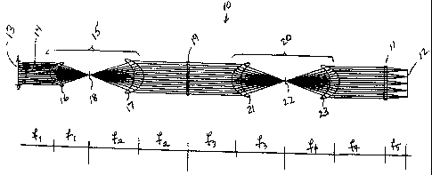
The optical train 10 of FIGURE 1 includes an entrance pupil 13 through
~s which is admitted a wavefront 14 for analysis. A first afocal relay system
15
comprises, for example, a pair of lenses comprising a first focusing, or -
converging, lens 16, and a first collimating lens 17. First collimating lens
17 is
positioned downstream of a first focal point 18 of the first focusing lens 16.
The
first afocal relay system 15 images the source of the incoming wavefront 14
onto
2o intermediate pupil plane 19.
Downstream of the intermediate pupil plane 19 is positioned a second
afocal relay system 20, formed, as in the first afocal relay system 15, by a
pair
of lenses comprising second focusing lens 21 having second focal point 22, and
zs second collimating lens 23. The second afocal relay system 20 images the
_g_
CA 02487018 2004-11-08
, ,
Ref: 2154US . . Exp~ : MaH No. EV 224559789 US
'intermediate pupil plane 19 onto a lenslet array 11 plane. The lenslet array
11
samples the wavefront 14 in a number of wavelets, which impinge onto the
detector 12 downstream of lenslet array 11. Respective focal lengths fy - f5
are
shown below the optical train 10 of FIGURE 1.
s
An alternate architecture for an optical train 30 is illustrated in FIGURE
2, this architecture requiring fewer elements and a smaller footprint. The
optical
train 30 includes an entrance pupil 31, and a first afocal relay system 100
comprising a pair of lenses. The lenses comprise a first focusing, or
converging,
lens 32, and a first collimating.lens 33. First collimating fens 33 is
positioned
downstream of a first focal point 34 of the first focusing lens 32. The first
collimating tens 33 receives a wavefront 35 from the first converging lens 32
at
a first face 36 and outputs a collimated wavefront 37 from a second face 38.
~s The first afocal relay system 100 of FIGURE 2 images the entrance pupil
31 onto intermediate pupil plane 39. A reflective optical element 40 is
positioned
at the intermediate pupil plane 39. Befinreen the lenses 32 and 33 is
positioned
a beamsplitter 41, which may comprise a pellicle beamsplitter, through which
the wavefront 35 exiting the first focusing lens 32 passes substantially
unaltered.
The reflective optical element 40 serves to reflect the wavefront 37 exiting
the first collimating lens 33 back through lens 33, the path of the reflected
wavefront 3T now reversed, so that the first collimating lens 33 also serves
as
a second converging lens. The reflected wavefront 37' is reflected by the
_g_
CA 02487018 2004-11-08
'Ref: 2154US Expr Mail No. EV 224559789 US
beamsplitter 41 toward a second collimating lens 42, where reflected wavefront
37' exits second collimating lens 42 as wavefront 43. Wavefront 43 impinges
upon a lensiet array 11. Focal lengths f, - f5 are shown in FIGURE 2 alongside
their respective optical path segments.
s
An optical train such as optical trains 10 and 30 described above, or
another such optical train as can be conceived by one of average skill in the
art,
can be used by the method and system of this invention to calibrate an
aberroscope, such as, but not intended to be limited to, a Hartmann-Shack
analyzer, including a lenslet array 11 and detector 12. In accordance with the
teachings of this invention, such an aberroscope calibration can be performed
using the optical element having a known aberration in the optical train 10
and/or
30. The optical element, an Aberroscope Calibration Device ("ACD°),
induces
a change of phase to a wavefront passing through or reflected by the optical
~s element, and has a phase surface modeled to reproduce a desired ocular
wavefront for transforming a parallel beam into the desired wavefront. Such an
optical element may comprise, but is not intended to be limited to, a lens
optimized for a specific power and aberration; a diffractive optical element
(DOE)
or computer-generated hologram (CGH); or a spatial light modulator (SLM), such
zo as a liquid crystal SLM, a Micro-Electro-Mechanical Systems (MEMS) device,
or
a continuous membrane deformable mirror. The optical element may be
transmissive or reflective.
The optical element (ACD) may be inserted into a wavefront
Zs measurement system at any of the following locations: the entrance pupil
plane;
-10-
CA 02487018 2004-11-08
rRaf: 2154US Expr Mail No. EV 224559789 US
the intermediate pupil plane; or the lenslet array plane. In prior art
systems,
calibration of an Aberroscope is required to be performed at a manufacturing
facility by introducing an aberrated wavefront at the entrance pupil plane.
The
embodiments of the present invention permit calibration to be performed at any
s time at an installed site without disturbing the Aberroscope installation.
Further,
the optical element of this invention may comprise a plurality of optical
elements
positionable one at a time in the optical train, such as, for example, by
using a
rotating turret holding the optical elements for serial insertion.
The ACD of the present invention can thus be used to perform
calibrationlvalidation of an instrument. For example, an ACD in a
monochromatic collimated or diverging beam provides, with high accuracy, a
wavefront containing a specific aberration (e.g., a Zemike spectrum).
Although,
theoretically, a phase function ~(x,y) can be introduced by either a
refractive or
~s a diffractive element and can be described in different mathematical forms,
it
may be determined that a particular CGH aberrator may be more easily designed
using a Zernike polynomial description.
Embodiments of the ACD of this invention can also be used to provide
2o discrete compensation, "shifting" the origin of measurement by a known
value.
As an example (see FIGURE 3), if a given wavefront measurement instrument
has a range R~ of measurement between -12D and +8D (the range of
measurement is determined mainly by first-order aberrations, i.e., defocus),
an
ACD capable of inducing a defocus of -6D will shift the range R~ to a new
range
2s R2 of measurement up to -18D (i.e., range R2 provides a range of
measurement
-11-
CA 02487018 2004-11-08
Ref: 2154US Expr Mail No. EV 224559789 US
from -18D to +2D). Similarly, an ACD capable of inducing a defocus of +6D will
shift the range R, to a new range R3, up to +14D (i.e., range R3 provides a
range
of measurement from -6D to +14D).
s Another embodiment of the method and system for Aberroscope
calibration and discrete compensation of the present invention includes
providing
continuous compensation using adaptive optical elements, such as a liquid
crystal SLM, a MEMS device, or a continuous membrane deformable mirror.
Continuous wavefront compensation/correction is very useful in some
applications related to detecting and measuring functional vision.
The accuracy of a wavefront aberration measurement in a Hartmann-
Shack analyzer is in part determined by the spot size produced by a lenslet on
the detector plane and by the separation between two adjacent spots. These
~s factors depend upon a number of parameters, including, in the case of an
eye
wavefront measurement, the spot size produced by the retinal probe beam,
sretina
Pupil diameter and pupil magnification are also important. For example,
Zo with reference to the optical train 10 of FIGURE 1, the pupil magnification
of the
wavefront measurement instrument is given by:
Mpupil = ~f2~f,) x ~f4~f3)
-12-
CA 02487018 2004-11-08
~ Ref: 2154US Expr . Mail No. EV 224559789 US
In the case of the optical train 30 of FIGURE 2, the pupil magnification
becomes:
Mp~p~~ = f~/f~, because f2 = f3
s
Also important are the Lenslet array effective focal length, denoted as f5
in FIGURES 1 and 2, the clear aperture of a lenslet, and the eye's aberration.
A paraxial approach to calculating the spot size at the lenslet array focal
to plane will be shown with reference to FIGURES 4-7. From the retina to the
object space (FIGURE 4):
y, 1000
~ D x EF e~~~ (Equation 1 )
The angle subtended by d~et,"a is:
retina
EFLemerrop (Equation 2)
Newton's equations show that (FIGURE 5):
Z x Z t _ - f 2 (Equation 3)
zo and
y r 2' f
y - f = Z (Equation 4)
-13-
CA 02487018 2004-11-08
~
Ref: 2154US Expr~ Mail No. EV 224559789 US
For an afocal relay system, the pupil magnification is (FIGURE 6):
Mp~p;i = f2/f~ (Equation 5)
The angular magnification between pupils is:
E'/E = 1/ MP"p;i (Equation 6)
Applying Newton's equations to the first and the second lenses, one obtains:
(Equation 7)
2 ~ 2
x zl~ - -f1 ~ Z2 x z2 = - f 2 z,~100/l~ z,'~ Z2~ -100 x ~~~p'~2
D l J
and
_Y2'= Y2~X Y~ = Z; x f2 ~ z,' - z2 Yi - M (Equation 8)
Y~ Yz Y~ f, zz ~ Yt PuPil
The spot size in the lenslet focal plane may be calculated as (FIGURE 7):
d (Equation 9)
a-2 (a+b)-EFLxE+EFLx ~Z2,~
where d is the lenslet size.
Equations 2, 6, and 7 then yield:
(Equation 10)
-14-
CA 02487018 2004-11-08
Ref: 2154US Expn ~ Mail No. EV 224559789 US
where:
8 =EFL x S'~tj"8 (Equation 11 )
EFLemetropx Mpupu
represents the retinal probe beam spot contribution to the spot size in the
lenslet
focal plane, and where:
Sb = EFL x d x p
1000 x M 2 Equation (12)
pupi
is the refractive ocular error contribution.
If an ACD is introduced into the optical path, whether in an intermediate
position or in front of the lenslet array, the eye aberration can be
dramatically
reduced, and by consequences the spot size on the detector plane, thereby
improving spot separation at the detector.
Several example calculations of an ACD are presented below.
~s Example 1. Lenses inducing pure defocus:
Lens type Power Clear Radius Conic ThicknessGlass
at apertureof constanton axis
820 nm curvature
Plano-concave-10D 12 mm -51.04 -0.58fi51.5 mm BK7
mm
Plano-convex+10D 12 mm 51.04 mm 0.582153 mm BK7
CA 02487018 2004-11-08
. ..
Ref: 2154US Exp~ Mail No. i=V 224559789 US
Example 2. Computer-generated holograms inducing spherical
aberration:
ACD type Clear aperture~=Azp2 + A4p4; Induced aberration
(mm) phase eq. of the in Terms of Zemike
Binary Surface Polynomials (gum)
(rad)
Negative spherical12 AZ=377 C4=-8.2
aberration A4=-377
Positive spherical12 A2=-377 C4=+8.2
aberration A4=377
s where p is the normalized radial aperture coordinate and the wavefront
equation
is WF=C4 (6p4-6p2-1 ).
Example 3. Computer-generated hologram inducing pure coma:
For a clear aperture: 12 mm and a=0.8 ,um, the phase equation of the binary
surface (in radians) is:
(Equation 13)
~(X~Y) - rM * ~IXZ + (Y + YO)2~a ' IX2 + ~Y ' Yo)212 - $ y03
where A4=202; r",r=6 mm, and yo=0.7 mm. The induced aberration in terms of
Zemike polynomials is (in Nm):
wF (X Y ) = 3 C2 (x2 y+~ )
rM
(Equation 14)
~s
where C3' _ -8.2.
-16-
CA 02487018 2004-11-08
,
Ref: 2154US Expr~. Mail No. EV 224559789 US
Using commercial optical-design software, the CGH can be modeled as
a diffractive surface defined by a phase function. The phase function is
specified
by an equation that could be a radial or Cartesian polynomial, a Zernike
s polynomial, or a Sweatt model phase equation. Basically, the optical
function
~(x,y) is determined by ray tracing from the ocular wavefront to be generated
to
the focal point of the setup. As the CGH null has to work in the first
diffraction
order, a carrier frequency must be added to the phase function in such a way
as
to ensure the separation of the diffraction orders. The CGH will be
appropriately
no titled or decentered with respect to the aberroscope axis.
Photolithography is probably the most commonly used technique for
making CGHs. Binary optics provides three main advantages: the capability of
producing complex diffractive structures; low production cost for two-phase-
level
~s elements; and the possibility of high diffraction efficiency with
multilevel
elements.
The phase function ~(x,y) reproduced by a diffractive binary element is
wrapped to an interval between 0 and an integral multiple of 2n. The phase
zo profile is given by:
y/(x,y~ -~~ (~y~-I-~~ ril0d 27t , (Equation 15)
where ~o is a constant phase offset. The two-level binary phase functions can
be described in various modes, for instance, ~b;nary(x) _ ~, when '/Z(xk +
Xk+~) <_
-17-
CA 02487018 2004-11-08
. ~ , ,
Ref: 2154US Exp~ ; Mail No. EV 224559789 US
are the solutions of the equations ~(xy) = 2k~ and ø(xy) _ (2k 1 ~,
respectively.
The surface-relief profile h(x,y) for a CGH etched on a substrate with a
refractive index n is given by:
h(x,y)= ~ ~b~nor~~Y) (Equation 16)
2~x n_1
s
Typically, a CGH is designed to operate at a specific wavelength.
Example 4. Combination of two lenses producing a known aberration.
FIGURE 8 illustrates a doublet 50 having the following specification: Entrance
pupil diameter =10 mm. The two elements are decentered t2 mm with respect
to the optical axis. The first element 51 is a plano-concave lens with a
radius of
curvature of 12.55 mm, a conic constant of 0.17, and a wedge (tilt) of
12°. The
second element 52 is a piano-convex lens with a biconic convex surface having
radii of curvature in two perpendicular planes of 15.23 mm and 15.05 mm. The
~s wavefront aberration produced by this doublet expressed in terms of Zernike
polynomials is:
Wl~~~=C3~'(3/.~-Z/~sifle+C,°(6p°-6~+1) , (Equation 17)
wherein the first term represents coma and the second, spherical aberration;
C3'=7.94; C4°= -0.234; and p is the normalized radial aperture
coordinate.
-18-
CA 02487018 2004-11-08
Ref: 2154US Expr- Mail No. EV 224559789 US
Example 5. Combination of two CGHs. In this example, a "doublet" of
two CGHs provides a specified amount of coma withouf spherical aberration, a
unique feature. For a clear aperture of 12 mm and ~I=0.82 Nm, the two CGHs
that are decentered t0.7 mm with respect to the optical axis have phase
s equations (in rad) given by:
~1 ( r) _ - 0.164 x r 4 (Equation 18)
~2 (r) _ +0.164. x r4 (Equation 19)
where r is the radial coordinate (in mm). The induced aberration in terms of
Zemike polynomials is (in,um):
-1 (Equation 20)
WF(X,Y) -~ (XZY+Y3)
rM
where C3' _ -8.65, rM = 6 mm; and X and Y are pupil coordinates (in mm).
A tolerance analysis related to the axial and transverse positioning of the
ACD can show the sensitivity to alignment/positioning parameters. Such an
analysis has been performed by the present inventor ("Ocular Aberrations
~s Induced by Centration Errors in Waveguided Treatments," The Association for
Research in Vision and Ophthalmology ("ARVO"), 2002).
Validation can be performed using an interferometric setup for any ACD
standalone, as well as for an entire wavefront measurement instrument
including
-19-
CA 02487018 2004-11-08
Ref: 2154US Expr Mail No. EV 224559789 US
the ACD. In this case, a flat mirror can be placed in front of the lenslet
array in
order to test the system in double-pass mode.
It may be appreciated by one of average skill in the art that the present
s invention confers the benefit of improved wavefront accuracy. Further,
compared with classical lenses that can generate limited types of ocular
aberration, such as defocus error and spherical aberration, a computer-
generated hologram can in principle reproduce any individual ocular aberration
or a combination of different aberrations to generate a composite wavefront.
In the foregoing description, certain terms have been used for brevity,
clarity, and understanding, but no unnecessary limitations are to be implied
therefrom beyond the requirements of the prior art, because such words are
used for description purposes herein and are intended to be broadly construed.
Moreover, the embodiments of the apparatus illustrated and described herein
are by way of example, and the scope of the invention is not limited to the
exact
details of construction.
Having now described the invention, the construction, the operation and
zo use of preferred embodiments thereof, and the advantageous new and useful
results obtained thereby, the new and useful constructions, and reasonable
mechanical equivalents thereof now obvious to those of average skill in the
art,
are set forth in the appended claims.
-20-
CA 02487018 2004-11-08