Note: Descriptions are shown in the official language in which they were submitted.
CA 02487819 2009-02-12
79150-60
1
BULK SILICON MIRRORS WITH HINGES UNDERNEATH
FIELD OF THE INVENTION
.(0002] This invention relates generally to micro-electro-mechanical systems
(MEMS). In
particular, it provides method and system for making MEMS mirrors by a
combination of bulk
and surface micromachining techniques.
BACKGROUND OF THE INVENTION
100031 MEMS mirrors have demonstrated to be effective in a variety of
applications,
including high-speed scanning and optical switching. In such applications, it
is essential for
MEMS mirrors to have flat optical surfaces, large rotational range, a4d robust
performance.
[0004] Many applications (e.g., optical networking applications) further
require that
MEMS mirrors be configured in a closely packed array. It is therefore
desirable to maximize
the "optical fill factor" of the array (i.e., by making the optical surface of
each constituent
mirror as large as possible), without compromising other essential
characteristics.
100051 MEMS mirrors are conventionally made by either bulk or surface silicon
micromachining techniques. Bulk micromachining, which typically produces
single-crystal
silicon mirrors, is known to have a number of advantages over surface
micromachining, which
typically produces polysilicon (or thin-film) mirrors. For example, single-
crystal silicon
mirrors produced by bulk micromachining techniques are generally thicker and
larger mirrors
with smoother surfaces and less intrinsic stress than polysilicon (or thin-
film) mirrors. Low
intrinsic stress and sizeable thickness result in flat mirrors, while smooth
surfaces reduce light
scattering. An advantage inherent to surface micromachining techniques is that
the mirror
suspension (e.g., one or more thin-film hinges) can be better defined and
therefore made
CA 02487819 2004-11-29
WO 03/102631 PCT/US03/16278
-2 -
smaller. This allows the MEMS mirror thus produced to have a large rotational
range, e.g., at
moderate drive voltages.
[0006] US Patent Number 6,028,689 of Michalicek et al. ("Michalicek et al.")
discloses a
movable micromirror assembly, driven by an electrostatic mechanism. The
assembly includes
a mirror supported by a plurality of flexure arms situated under the mirror.
The flexure arms
are in turn mounted on a support post. Because the assembly disclosed by
Michalicek et al. is
fabricated entirely by way of surface micromachining techniques, the resulting
"micromirror"
is of the polysilicon (thin-film) type and is thus subject to the
aforementioned disadvantages.
[0007] International Patent Application Number WO 01/94253 A2 of Chong et al.
discloses a MEMS mirror device having a bulk silicon mirror attached to a
frame by thin-film
hinges. A notable shortcoming of this system is evident in that the thin-film
hinges extend
from the reflective surface side of the mirror to the frame, hence restricting
(or obstructing) the
amount of surface area available for optical beam manipulation. This
shortcoming further
results in a lower optical fill factor in an array of such MEMS devices.
[0008] Tuantranont et al. disclose an array of deflectable mirrors fabricated
by a surface
micromachining polysilicon (or "MUMPS") process in "Bulk-Etched Micromachined
and
Flip-Chip Integrated Micromirror Array for Infrared Applications," 2000
IEEE/LEOS
International Conference on Optical MEMS, 21024, Kauai, Hawaii (August 2000).
In this
case, an array of polysilicon mirror plates is bonded to another array of
thermal bimorph
actuators by gold posts using the "flip-chip transfer technique", resulting in
trampoline-type
polysilicon plates each suspended at its corners by thermal bimorph actuators.
In addition to
the mirror plates made of polysilicon (or thin-film), another drawback of the
thus-constructed
mirror array is the lack of a monolithic structure, which makes the array
susceptible to
misalignment and other extraneous undesirable effects.
[0009] In view of the foregoing, there is a need in the art to provide a novel
type of MEMS
mirrors that overcomes the limitations of prior devices in a simple and robust
construction.
SUMMARY OF THE INVENTION
[0010] The present invention provides a MEMS apparatus, including a bulk
element; a
support; and one or more hinges. The bulk element comprises a device surface
and a bottom
CA 02487819 2004-11-29
WO 03/102631 PCT/US03/16278
-3 -
surface that is situated below the device surface. The hinges are disposed
below the bottom
surface of the bulk element and couple the bulk element to the support,
whereby the bulk
element is suspended from the support.
[00111 In the above apparatus, the support may include a cavity, in which the
hinges are
disposed. There may be at least one electrode disposed in the cavity, for
causing the bulk
element to be actuated. The device surface of the bulk element may further
contain a reflective
layer (e.g., a metallic film), rendering the apparatus thus constructed a MEMS
mirror.
[0012] In the present invention, the term "bulk element" refers to an element
fabricated by
bulk micromachining techniques known in the art, which typically comprises a
single-crystal
material. A case in point may be a single-crystal silicon element. The bulk
element is
characterized by a "device" surface and a "bottom" surface that is situated
below the device
surface (while the bulk element itself may assume any geometric form deemed
suitable). The
"device" surface of the bulk element may be optically reflective. It may also
be used as an
"interface" for coupling the bulk element to other devices, if so desired in a
practical
application. Further, a "support" may be a frame or substrate, to which the
bulk element is
attached. A "hinge" (or "hinge element") should be construed broadly as any
suspension/coupling means that enables the bulk element to be suspended from
the support and
further provides the restoring force as the bulk element undergoes motion. For
instance, a
hinge may be a flexure or flexible coupling, e.g., fabricated by a bulk or
surface
micromachining technique known in the art. The term "underneath" refers to the
hinges being
anchored to (or below) the bottom surface of the bulk element and thereby
disposed wholly
beneath the device surface. This allows the device surface of the bulk element
to be
maximized and the entire surface to be usable (e.g., for optical reflection).
[0013] The present invention further provides a process flow (or method) that
may be used
for fabricating the aforementioned MEMS apparatus. In one embodiment of a
process flow
according to the present invention, a "device" component is formed. The device
component in
one form may be provided by an SOI (Silicon-On-Insulation) wafer, comprising a
single-
crystal silicon device layer and a silicon handle wafer with an insulation
layer (e.g., silicon
oxide) sandwiched in between. First and second hinge elements may be
fabricated on a first
surface of the single-crystal silicon layer, e.g., by way of surface
micromachining techniques.
A "support" component is configured to contain a cavity, in which at least one
electrode may
CA 02487819 2009-02-12
79150-60
-4 -
be disposed. Subsequently, the device and support components are bonded in
such a manner
that the hinge elements are disposed within the cavity. The silicon handle
wafer along with the
insulation layer in the device component is then removed, thereby revealing a
second surface
of the single-crystal silicon device layer. A bulk element may be subsequently
produced in the
single-crystal silicon device layer by way of bulk micromachining techniques,
characterized by
the first and second surfaces. The configuration may be such that the hinge
elements are each
anchored to the first (or "bottom") surface of the bulk element on one end and
to the support
component on the other, thereby enabling the bulk element to be suspended with
the hinge
elements wholly undemeath the second (or "device") surface. A reflective layer
may be
further deposited on the device surface of the bulk element, rendering the
apparatus thus
constructed a MEMS mirror.
[0014] One advantage of the MEMS apparatus of the present invention is that by
placing
the hinge elements underneath the bulk.element, the device surface of the bulk
element can be
maximized and the entire surface becomes usable (e.g., for optical beam
manipulation). Such a
feature would be highly advantageous in making arrayed MEMS devices, such as
an array of
MEMS mirrors with a high optical fill factor. Further, by advantageously
making use of both
bulk and surface micromachining techniques, a MEMS mirror of the present
invention is
equipped with a large and flat mirror along with flexible hinges, and is hence
capable of
achieving a substantial rotational range at moderate electrostatic drive
voltages. An additional
advantage of the MEMS apparatus of the present invention is evident in its
monolithic
structure, rendering it robust in performance. These advantageous features are
in notable
contrast with the prior devices described above.
CA 02487819 2009-02-12
79150-60
4a
The invention also relates to an optical apparatus
comprising: a) a bulk element having an optical surface, a
bottom surface, disposed below said optical surface, and a base
portion which extends downward from said bottom surface; b) a
support, including a cavity formed by a plurality of sidewalls;
and c) first and second hinge elements, which are disposed
wholly below said bottom surface, and which are directly
coupled to said base portion and to a pair of said sidewalls,
effective to suspend said bulk element from said support.
The invention further relates to an optical apparatus
comprising: a plurality of MEMS devices configured in an array,
wherein each MEMS device includes: a) a bulk element having an
optical surface, a bottom surface, disposed below said optical
surface, and a base portion which extends downward from said
bottom surface; b) a support, including a cavity formed by a
plurality of sidewalls; and c) first and second hinge elements,
which are disposed wholly below said bottom surface, and which
are directly coupled to said base portion and to a pair of said
sidewalls, effective to suspend said bulk element from said
support.
The invention still further relates to a method of
making a MEMS apparatus, comprising: a) providing a device
component comprising single-crystal silicon; b) creating at
least one hinge in said device component; c) constructing a
support component having a cavity; d) bonding said device
component to said support component, such that said at least
one hinge is disposed within said cavity; and e) forming in
said device component a bulk element having a device surface
and a bottom surface, whereby said at least one hinge is
coupled to said bulk element and is disposed below said bottom
surface, thereby suspending said bulk element from said
support.
CA 02487819 2009-02-12
79150-60
4b
[0015J The novel features of this invention, as well as the invention itself,
will be best
understood from the following drawings and detailed description.
BRIEF DESCRIPTION OF THE FIGURES
100161 FIG. 1A is a schematic side sectional view of a first embodiment of a
MEMS
apparatus, according to the present invention;
100171 FIG. 1B is a schematic top view of a first embodiment of a MEMS
apparatus,
according to the present invention;
[0018[ FIG. 2 is a schematic side sectional view of a second embodiment of a
MEMS
apparatus, according to the present invention;
CA 02487819 2004-11-29
WO 03/102631 PCT/US03/16278
-5 -
[0019] FIG. 3 is a schematic side sectional view of a third embodiment of a
MEMS
apparatus, according to the present invention; and
[0020] FIGS. 4A-4F show an exemplary process flow for fabricating a MEMS
apparatus,
according to the present invention.
DETAILED DESCRIPTION
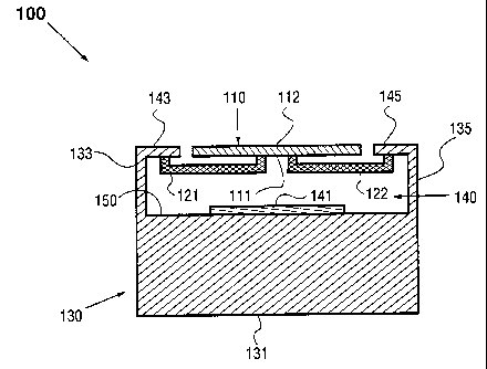
[0021] FIGS. lA-1B illustrate a first embodiment of a MEMS apparatus,
according to the
present invention. FIG. 1A depicts a schematic side sectional view of a MEMS
apparatus 100,
comprising a bulk element 110; first and second hinge elements 121, 122; and a
support 130.
The bulk element 110 may have a "device" (or "top") surface 112, and a
"bottom" surface 111
which is disposed below and opposes the device surface 112. The first and
second hinge
elements 121, 122 are each disposed below the device surface 112. As a way of
example in the
embodiment of FIG. 1A, the hinge elements 121, 122 are each coupled to the
bottom surface
111 of the bulk element 110 on one end and to the support 130 on the other. In
this manner,
the bulk element 110 is suspended with the hinge elements 121, 122 disposed
wholly
underneath the device surface 112.
[0022] FIG. 1B shows a schematic top view of the MEMS apparatus 100. By way of
example, the device surface 112 of the bulk element 110 is shown to be
generally rectangular
in shape. It will be appreciated that this need not be case; in fact, the
device surface of a bulk
element (or the bulk element itself) in the present invention may assume any
geometric form
(e.g., elliptical) that is deemed suitable for a given application.
[0023] In the embodiment of FIGS. 1A-1B, the support 130 may include a
substrate
portion 131 and a cavity 140. By way of example, the substrate portion 131 may
be generally
rectangular in shape. A plurality of sidewalls 132, 133, 134, 135 may extend
from the portion
131 and thereby form the cavity 140. As shown in FIG. 1A, the hinge elements
121, 122 are
disposed within the cavity 140, and are coupled respectively to the sidewalls
133, 135. In the
embodiment of FIGS. 1A-1B, each of the sidewalls 132, 133, 134, 135 may
include a
corresponding ridge (or "lip") portion 142, 143, 144, 145 that projects inward
from the
respective sidewall (see the ridge portions 143, 145 shown in FIG. 1A, for
example).
Furthermore, the hinge elements 121, 122 have a generally "C"-shaped (side-
view) cross-
section, and are coupled to the ridge portions 143, 145 of the sidewalls 133,
135, respectively.
However, this should not be viewed as limiting in any way. For example, in
alternate
CA 02487819 2004-11-29
WO 03/102631 PCT/US03/16278
-6-
embodiments, the hinge elements 121, 122 may assume any other suitable shape
or cross-
section. They may also be coupled to other portions of the sidewalls 133, 135.
[0024] In the embodiment shown in FIGS. 1A-1B, the cavity 140 is shown to be
generally
rectangular in shape. However, in alternate embodiments, the cavity 140 may
assume any
other suitable geometric form. The cavity 140 may include at least one
electrode 141, which
may be disposed on a bottom surface 150 of the cavity 140. The electrode 141
is adapted to
cause the bulk element 110 to be actuated in a known manner (e.g., in an
electro-static
fashion). Moreover, the device surface 112 of the bulk element 110 may be
optically
reflective, e.g., by way of polishing and/or depositing a metallic film on the
surface.
[0025] FIG. 2 shows a schematic side sectional view of a second embodiment of
a MEMS
apparatus. By way of example, MEMS apparatus 200 may comprise a bulk element
210; first
and second hinge elements 221, 222; and a support 230. The bulk element 210
may include a
"device" (or "top") surface 212, and a "bottom" surface 211 which is disposed
below and
opposes the device surface 212. In this embodiment, the bulk element 210 may
further include
a base portion 215, which may extend downward from the bottom surface 211. The
first and
second hinge elements 221, 222 are each disposed below the device surface 212.
As a way of
example, the first and second hinge elements 221, 222 are each shown to be
coupled to the
base portion 215 of the bulk element 110 on one end and to the support 130 on
the other. In
this manner, the bulk element 210 is suspended with the hinge elements 221,
222 disposed
wholly underneath the device surface 212.
[0026] In the embodiment of FIG. 2, the support 230 may include a substrate
portion 231
and a cavity 240. By way of example, the substrate portion 231 may be
generally rectangular
in shape. A plurality of sidewalls 233, 235 extend from the portion 231 and
thereby form the
cavity 240. The hinge elements 221, 222 are disposed within the cavity 240. In
the present
embodiment, the hinge elements 221, 222 may extend in a generally horizontal
direction,
thereby coupling the base portion 215 to the sidewalls 233, 235, respectively.
However, this
should not be viewed as limiting in any way. For example, in alternate
embodiments, the
hinge elements 221, 222 may assume any other suitable shape. They may also be
positioned in
other directions, and/or coupled to other portions of the sidewalls 233, 235.
CA 02487819 2004-11-29
WO 03/102631 PCT/US03/16278
-7 -
[0027] The cavity 240 may be of any suitable shape in the embodiment of FIG.
2. The
cavity 240 may include at least one electrode 241, which may be disposed on a
bottom surface
250 of the cavity 240. The electrode 241 is adapted to cause the bulk element
210 to be
actuated in a known manner (e.g., electro-statically). The device surface 212
of the bulk
element 210 may likewise be optically reflective, e.g., by way of polishing
and/or depositing a
metallic film on the surface.
[0028] FIG. 3 shows a schematic side sectional view of a third embodiment of a
MEMS
apparatus 300. With the exception of a bulk element 310, MEMS apparatus 300 is
shown to be
substantially similar to the MEMS apparatus 200, and may make use of the
general
configuration of and a number of the elements shown in FIG. 2. As shown in
FIG. 3, the
MEMS apparatus 300 may comprise a bulk element 310; first and second hinge
elements 321,
322; and a support 330. The support 330 may include a cavity 340, which is
formed by at least
two sidewalls 333, 335 that extend from substrate portion 331. The cavity 340
may include a
bottom surface 350, on which at least one electrode 341 may be disposed.
[0029] In the MEMS apparatus 300, the bulk element 310 may include a "device"
(or
"top") surface 312, and a "bottom" surface 311 which is disposed below and
opposes the
device surface 312. As a way of example, the bulk element 310 is shown to
include a
generally "T"-shaped base portion 315. The base portion 315 extends downward
from the
bottom surface 311 and forms side cavities or "voids" 316, 317 in the bulk
element 310. As in
the embodiment of FIG. 2, the first and second hinge elements 321, 322 are
each disposed
beneath the bottom surface 311 of the bulk element 310. In the present
embodiment, the hinge
elements 321, 322 are each shown to be coupled to the base portion 315 of the
bulk element
310 within the respective voids 316, 317 on one end and to the respective
sidewalls 333, 335 of
the support 330 on the other. In this manner, the bulk element 310 is
suspended with the hinge
elements 321, 322 disposed wholly underneath the device surface 312.
[0030] In the foregoing embodiments and in an exemplary fabrication process
described
below, the term "bulk element" (e.g., the bulk element 110, 210, or 310)
refers to an element
fabricated by bulk micromachining techniques known in the art, which typically
comprises a
single-crystal material. For example, the bulk elements 110, 210, 310 shown
above may each
be a single-crystal silicon element. The bulk element is characterized by a
"device" surface
and a "bottom" surface that is situated below the device surface; while the
bulk element itself
CA 02487819 2004-11-29
WO 03/102631 PCT/US03/16278
-8-
may assume any geometric form that is appropriate for a given application. (It
will be
appreciated that the device and bottom surfaces need not be opposing one
another, in general.)
The "device" surface of a bulk element may be optically reflective. An optical
element (e.g., a
grating) may also be patterned on it. Additionally, the device surface may be
used as an
"interface" for coupling the bulk element to other devices, if so desired in
practical
applications.
[0031] Further, a "support" (e.g., the support 130, 230, or 330) may be a
frame or
substrate, to which the bulk element is attached. A "hinge" (or "hinge
element") should be
construed broadly as any suspension/coupling means that enables the bulk
element to be
suspended from the support and further provides the restoring force as the
bulk element
undergoes motion (e.g., due to the actuation mechanism caused by the electrode
141 of FIGS.
1A-1B). As a way of example, the first or second hinge element shown in FIG.
1A, 2, or 3
may be a flexure or flexible coupling, e.g., fabricated by bulk or surface
micromachining
techniques known in the art. While two hinge elements are shown in each of the
foregoing
embodiments, alternate embodiments may include a fewer or greater number of
hinge
elements. The term "underneath" refers to a hinge element being anchored to
(or below) the
bottom surface of the bulk element and thereby disposed wholly beneath the
device surface.
This allows the device surface of the bulk element to be maximized and the
entire surface to be
usable (e.g., for optical beam manipulation), as the above embodiments
illustrate.
[0032] FIGS. 4A-4F show an exemplary embodiment of a process flow, which may
be
utilized for fabricating a MEMS apparatus (e.g., the embodiment of FIGS. 1A-
1B) according
to the present invention. FIG. 4A shows a schematic side sectional view of a
"device"
component 400, which in one form may be an SOI (Silicon On Insulator) wafer,
comprising a
single-crystal silicon "device" layer 415 and a silicon "handle wafer" 417
with a first insulation
layer 416 (e.g., silicon oxide) sandwiched therein between. The single-crystal
silicon device
layer 415 may have a predetermined thickness d, which may be on the order of 5-
100 m.
First and second hinge elements 421, 422 are fabricated on a first surface 411
of the single-
crystal silicon device layer 415 in a known manner, e.g., by a known surface
micromachining
technique. Each hinge element may be a thin-film, e.g., composed of
polysilicon, polyoxide,
nitride, silicon nitride, silicon oxide, silicon oxynitride, or a metal. First
and second
"sacrificial" elements 423, 424 (which may be formed from silicon oxide) may
be first
CA 02487819 2004-11-29
WO 03/102631 PCT/US03/16278
-9-
patterned on the first surface 411, prior to forming the first and second
hinge elements 421,
422, respectively.
[0033] FIG. 4B shows a schematic side sectional view of a "support" component
450
containing an "open-ended" cavity 440. As a way of example, the cavity 440 may
be formed
by a substrate wafer 431 and a plurality of spacers 433, 435 which form
sidewalls of the cavity
440. There may be at least one electrode 441 disposed in the cavity 440, e.g.,
patterned on the
substrate wafer 431 via a second insulation layer 432 which may be made of
silicon oxide.
[0034] Referring now to FIG. 4C. The device component 400 formed in FIG. 4A is
bonded with the support component 450 of FIG. 4B in such a manner that the
first and second
hinge elements 421, 422 are disposed (or accommodated) within the cavity 440.
In the next
step of the fabrication process flow, illustrated in FIG. 4D, the silicon
handle wafer 417 (along
with the first insulation layer 416) is removed, thereby revealing a second
surface 412 of the
single-crystal silicon device layer 415.
[0035] In the subsequent step of the fabrication process flow, depicted in
FIG. 4E, a "bulk
element" 410 is formed in the single-crystal silicon device layer 415 by a
known bulk
micromachining technique (e.g., a DRIE (Deep Reactive Ion Etching) process)
known in the
art. The formed bulk element 410 is also characterized by the first and second
surfaces 411,
412 that oppose one another. In the next step of the fabrication process flow,
shown in FIG.
4F, the bulk element 410 is "released", e.g., by removing the first and second
sacrificial
elements 423, 424. Note that the remainder of the single-crystal silicon
device layer 415, the
spacers 433, 435, and the support wafer 431 form an integrated support
structure 430, which
may substantially constitute the support 130 in the embodiment of FIGS. 1A-1B,
for instance.
(Those skilled in the art will appreciate that first and second sacrificial
elements 423, 424 may
also be removed earlier, e.g., anywhere in the fabrication process flow after
the step of FIG.
4A.)
[0036] A reflective layer 402 (e.g., a gold film) may be further deposited on
the second
surface 412 of the bulk element 410, rendering the apparatus thus constructed
a MEMS mirror.
Note that because the first and second hinge elements 421, 422 are anchored to
the first (or
"bottom") surface 411 and thereby wholly "underneath" the bulk element 410
thus produced,
the second (or "device") surface 412 of the bulk element 410 can be maximized
and the entire
CA 02487819 2004-11-29
WO 03/102631 PCT/US03/16278
-10-
surface becomes usable (e.g., for optical reflection). Furthermore, being
situated in a cavity
(e.g., the cavity 440), the first and second hinge elements 421, 422 can be
made sufficiently
long/large, if so desired in a given application.
[0037] In the aforementioned process flow, use of an SOI wafer for the device
component
400 of FIG. 4A has the advantages of providing precise control of the
thickness of the bulk
element 410 (by way of the predetermined thickness d of the single-crystal
silicon device layer
of the SOI wafer) and ease in manipulation (owing to the handle wafer of the
SOI wafer),
while the intervening insulation layer of the SOI wafer may serve as a
convenient "etch-stop"
(e.g., when removing the handle wafer). The hinge elements may also be
fabricated by a
known bulk micromachining technique (e.g., the SCREAM (Single Crystal Reactive
Etching
and Metallization) process known in the art). It will be appreciated, however,
that a device
component in the present invention may alternatively be formed in an epitaxial
silicon wafer,
or a single piece of single-crystal silicon, where the hinge elements may be
fabricated in a
manner similar to that described above.
[0038] The support component 450 of FIG. 4B may likewise be fabricated out of
an SOI
wafer which may be similar to that shown in FIG. 4A in configuration. As a way
of example,
the silicon device layer (e.g., 50 - 100 m in thickness) of the SOI wafer may
be used to form
the spacers 433, 435 along with the electrode 441 (e.g., by way of etching),
while the
corresponding handle wafer may serve as the substrate wafer 431.
Alternatively, a glass wafer
may be used to form the substrate wafer 431, on which the electrode 441 may be
deposited
(e.g., by a known surface micromachining technique) and the spacers 433, 435
(e.g., made of
silicon) bonded. The support component 450 of FIG. 4B may also be fabricated
out of a single
piece of a desired material (e.g., a silicon or glass wafer) using an
appropriate technique known
in the art. Those skilled in the art will appreciate that a support component
in the present
invention may generally be configured in any way that is suitable for a given
application; what
is important is that the support element thus configured contains an open-
ended cavity (so as to
host the hinge elements), e.g., in a manner as illustrated with respect to
FIG. 4B.
[0039] A distinct feature of the fabrication process flow of FIGS. 4A-4F is
that the device
component 400 and the support component 450 are bonded in such a manner that
the hinge
elements are disposed within (or accommodated by) the cavity 440 of the
support component
450 (e.g., see FIG. 4C above), thereby allowing the hinge elements to be
situated "underneath"
CA 02487819 2004-11-29
WO 03/102631 PCT/US03/16278
-11-
the bulk element thus produced. One skilled in the art will know how to apply
a suitable
process known in the art that is effective for carrying out the requisite
bonding (e.g., fusion or
anodic bonding). It will be appreciated that various elements in the
embodiment of FIGS. 4A-
4F are shown as a way of example to illustrate the general principles of the
present invention,
and therefore are not drawn to scale (e.g., in either geometric shape or
size). From the teaching
of the present invention, those skilled in the art will know how to implement
the fabrication
process flow of FIGS. 4A-4F in a given application, to produce a suitable MEMS
apparatus
according to the present invention.
[0040] An advantage of the MEMS apparatus of the present invention is that by
placing the
hinge elements underneath the bulk element, the device surface of the bulk
element can be
maximized and the entire surface becomes usable (e.g., for optical beam
manipulation). Such a
feature would be highly advantageous in making arrayed MEMS devices, such as
an array of
MEMS mirrors with a high optical fill factor. Further, by advantageously
making use of a
combination of bulk and surface micromachining techniques, a MEMS mirror
according to the
present invention may be equipped with a large and flat mirror along with
flexible hinges,
thereby capable of providing a substantial rotational range at moderate
electrostatic drive
voltages. An additional advantage of the MEMS apparatus of the present
invention is evident
in its monolithic structure, rendering it robust in performance. These
advantageous features
are in notable contrast with the prior devices described above. As such, the
present invention
may be used in a variety of applications, e.g., providing arrayed MEMS mirrors
(or beam
steering devices) for optical networking applications.
[0041] Those skilled in the art will recognize that the exemplary embodiments
described
above are provided by way of example to illustrate the general principles of
the present
invention. Various means and methods can be devised herein to perform the
designated
functions in an equivalent manner. Moreover, various changes, substitutions,
and alternations
can be made herein without departing from the principles and the scope of the
invention.
Accordingly, the scope of the present invention should be determined by the
following claims
and their legal equivalents.