Note: Descriptions are shown in the official language in which they were submitted.
CA 02488054 2004-12-O1
Description
OPTICAL SWITCH
Technical Field
The present invention relates to an optical switch which
serves to change over the coupling relationship between an input
optical path (for example, an input optical fiber) and an output
optical path (for example, an output optical fiber).
Background Art
In the field of optical communication, an optical switch
is used for changing over an optical fiber transmission path
or a light transmission/reception terminal device or the like.
Views shown in Fig. 1(a) and Fig. 1(b) are a plan view and a
cross-sectional view for explaining the structure of a main
part of a 2x2 type optical switch which has been proposed
conventionally. In this optical switch, a recessed portion
3 is formed in a flat-panel like switch board 2 and a first
and second light reflection surfaces 4, 5 are formed on inner
surfaces of the recessed portion 3 such that these reflection
surfaces 4, 5 make an angle of 90 degrees . Further, an elongated
resilient member 6 is formed on a bottom surface of the switch
board 2 in a cantilever manner, wherein a distal end of the
resilient member 6 having resiliency is fixed to a cubic movable
1
CA 02488054 2004-12-O1
reflection member 7. The movable reflection member 7 is
arranged to be positioned in an inner corner portion constituted
by the first and second light reflection surfaces 4, 5 . Further,
a third and fourth light reflection surfaces 8, 9 are formed
on two neighboring surfaces of the movable reflection member
7 . The resilient member 6 is configured, as shown in Fig. 1 (b) ,
bendable in the up-and-down directions and the movable
reflection member 7 which is positioned in the inner corner
portion of the first and second light reflection surfaces 4
is lowered more downwardly than the first and second light
reflection surfaces 4, 5 along with the downward bending of
the resilient member 6. Although not shown in the drawings,
an electromagnet is arranged below the switch board 2, wherein
when the electromagnet is energized, the resilient member 6
is attracted downwardly and hence, the movable reflectionmember
7 is lowered downwardly, while when the electromagnet is
deenergized, the resilient member 6 is attracted upwardly and
hence, the resilient member 6 returns upwardly whereby the
movable reflection member 7 returns in front of the first and
second light reflection surfaces 4, 5.
Fig. 2(a), (b) are views for explaining the changeover
operation of the above-mentioned optical switch. In this
example, a first input optical fiber 10 is arranged to face
the first light reflection surface 4 in an opposed manner, a
second input optical fiber 11 is arranged to face the fourth
2
CA 02488054 2004-12-O1
light reflection surface 9 in an opposed manner, a first input
optical fiber 12 is arranged to face the third light reflection
surface 8 in an opposed manner, and the second input optical
fiber 13 is arranged to face the second light reflection surface
in an opposed manner.
Here, when the movable reflection member 7 is elevated
and is positioned in front of the first and second light
reflection surfaces 4, 5, as shown in Fig. 2(a), a light 14
radiated from the first input optical fiber 10 is reflected
on the first light reflection surface 4 and the third light
reflection surface 8 and, thereafter, is coupled to the first
output optical fiber 12. A light 15 radiated from the second
input optical fiber 11 is reflected on the fourth light
reflection surface 9 and the second light reflection surface
5 and, thereafter, is coupled to the second output optical fiber
13.
Further, when the movable reflection member 7 is lowered
and is not positioned in front of the first and second light
reflection surfaces 4, 5, as shown in Fig. 2 (b) , the light 14
radiated from the first input optical fiber 10 is reflected
on the first light reflection surface 4 and the second light
reflection surface 5 and, thereafter, is coupled to the second
output optical fiber 13. The light 15 radiated from the second
input optical fiber 11 is reflected on the second light
reflection surface 5 and the first light reflection surface
3
CA 02488054 2004-12-O1
4 and, thereafter, is coupled to the first output optical fiber
12.
Accordingly, in the optical switch having such a
constitution, by elevating and lowering the movable reflection
member 7 by driving the resilient member 6 with the electromagnet,
the coupling destinations of the lights radiated from the first
input optical fiber 10 and the second input optical fiber 11
can be changed over between the first output optical fiber 12
and the second output optical fiber 13.
However, in the optical switch having such a structure,
since the first and second light reflection surfaces 4, 5 and
the third and fourth light reflection surfaces 8, 9 are formed
on different members (inner surfaces of the recessed portion
of the switch board 2 and the movable reflection member 7),
in an assembling step of the optical switch and at the time
of coupling the optical switch and the optical fiber, the
positioning of the respective light reflection surfaces and
the optical fiber becomes extremely cumbersome and hence, these
operations become difficult to perform.
To explain the above more specifically, it is as follows.
First of all, in a state before mounting the movable reflection
member 7 on the resilient member 6, the first and the second
input optical fibers 10, 11 and the first and the second output
optical fibers 12, 13 are arranged parallel to each other and,
thereafter, as shown in Fig. 2(b), the positions of centers
4
CA 02488054 2004-12-O1
of four optical fibers 10, 11, 12, 13 are aligned with each
other for every combination of inputting and outputting of lights
such that the light 15 which is radiated from the second input
fiber 11 is incident on the first output optical fiber 12 and
the light 14 which is radiated from the first input optical
fiber 10 is incident on the second output optical fiber 13 and,
in a past center-alignment state, the respective optical fibers
10, 11, 12, 13 are fixed by solidifying them with an adhesive
agent or the like. Next, the movable reflection member 7 is
arranged in front of the second input optical fiber 11 and the
first output optical fiber 12 and a position and an angle of
the movable reflection member 7 are adjusted by moving the
movable reflection member 7. As shown in Fig. 2 (a) , when the
position and the angle of the movable reflection member 7 are
adjusted with respect to the respective optical fibers 10, 11,
12 and 13 such that the light 14 radiated from the first input
optical fiber 10 is incident on the first output optical fiber
12 and the light 15 radiated from the second input optical fiber
11 is incident on the second output optical fiber 13, the movable
reflection member 7 is fixed to an upper surface of the distal
end portion of the resilient member 6 using an adhesive agent
or the like while holding the state.
However, in the state that the movable reflection member
7 is not yet mounted on the resilient member 6, the centers
of the respective optical fibers 10, 11, 12 and 13 are aligned
CA 02488054 2004-12-O1
with each other and, thereafter, the respective optical fibers
10, 11, 12 and 13 are fixed. Accordingly, in the adjustment
of the position and the angle of the movable reflection member
7 in front of the optical fibers 11, 12, the positional
relationship among the optical fibers 10, 11, 12 and 13 cannot
be changed and hence, it is difficult to adjust the position
and the angle of the movable reflection member 7 with high
accuracy. Further, when there exist irregularities with
respect to the positions of the first light reflection surface
4 and the second light reflection surface 5, there also arise
the irregularities with respect to the positions of the optical
fibers 10, 11, 12 and 13 which are determined by reference to
the light reflection surfaces 9, 5 and hence, the adjustment
of the position and the angle of the movable reflection member
7 become further complicated. Accordingly, with respect to
the optical switch having such a structure, before and after
mounting the movable reflection member 7, it is necessary to
adjust the positions of the optical fibers 10, 11, 12 and 13
and the position and the angle of the movable reflection member
7 in a trial-and-error manner thus making the assembling of
the optical switch difficult.
Disclosure of the Invention
The invention has been made in view of such circumstances
and it is an obj ect of the invention to enable the simple alignment
6
CA 02488054 2004-12-O1
of axes of an input optical path, an output optical path and
a light reflection surface in an optical switch for changing
over an input optical path and an output optical path.
The optical switch according to the invention is an optical
switch including at least three input and output optical paths
in total and performing the changeover of the optical paths
by changing the combination of the input optical path and the
output optical path which transmit light to each other, wherein
a first region in which a front surface of a mirror member which
is movable relative to the input optical path and the output
optical path is allowed to face the input optical path and the
output optical path thus forming a pair of light reflection
surfaces which cross each other with a given angle, and a second
region in which a plural pairs of light reflection surfaces
are formed in a state that the neighboring light reflection
surfaces cross each other with given angles, are arranged in
front of the mirror member and along the moving direction of
the mirror member.
Here, the input optical path is a light transmissionmedium
which allows the light to perform the transmission propagation
and irradiates light into a space and is, for example,
constituted of an optical fiber or an optical waveguide . The
output optical path is a light transmission medium which allows
the light incident from the space to perform the transmission
propagation and is, for example, constituted of an optical fiber
7
CA 02488054 2004-12-O1
or an optical waveguide.
According to the optical switch of the invention, for
example, when both of the input optical path and the output
optical path are provided in a plural number respectively, as
in a case of embodiments of the invention, the lights which
are radiated from some input optical paths among the plurality
of input paths are incident on some output optical path among
the plurality of output optical paths by being reflected on
the light reflection surfaces formed in the first region and
the lights which are radiated from another input optical paths
are incident on another output optical path by being reflected
on the light reflection surfaces formed in the first region,
while the lights which are radiated from some input optical
paths among the plurality of input optical paths are incident
on another output optical path among the plurality of output
optical paths by being reflected on the light reflection surfaces
formed in the second region and lights which are radiated from
another input optical paths are incident on some output optical
path by being reflected on the light reflection surfaces formed
in the second region. Due to such a constitution, by changing
over the region where the lights are reflected by relatively
moving the mirror member between the first region and the second
region, it is possible to change over the coupling relationship
of the input optical path and the output optical path. (Here,
in the description of the embodiments, the optical switch of
8
CA 02488054 2004-12-O1
the invention does not exclude a case in which either one of
the number of the input optical paths and the number of the
output optical paths is set one and a case in which the number
of the input optical paths and the number of the output optical
paths are not equal).
Further, in this optical switch, the first region where
the pair of light reflection surfaces are formed and the second
region where the plural pairs of the light reflection surfaces
are formed are integrally formed on the mirror member and hence,
the positional displacement and the angular error between the
light reflection surfaces of the first region and the light
reflection surfaces of the second region depend on only the
accuracy of parts (not influenced by assembling) whereby the
positional displacement and the angular error are extremely
small and stable . Accordingly, it is possible to easily perform
the positional adjustment operation of the input optical path,
the output optical path and the respective light reflection
surfaces.
The optical switch according to another mode of the
invention, the optical switch includes an actuator for moving
the mirror member and hence, it is possible to change over the
optical switch in response to an electric signal.
In the optical switch according to still another mode
of the invention, portions of the input optical path and the
output optical path which face the front surface of the mirror
9
CA 02488054 2004-12-O1
member are integrally formed with each other and hence, it is
sufficient to perform only the adjustment of the whole input
optical path and output optical path and the mirror member
whereby it is possible to perform the positional adjustment
operation more easily.
Further, the optical switch according to still another
mode of the invention includes means which monitors which one
of the first region and the second region among the front surface
of the mirror member faces the input optical path and the output
optical path and hence, it is possible to know the changeover
state of the optical switch in response to an electric signal,
for example, via the monitoring means.
In the optical switch according to still another mode
of the invention, a spatial optical path length from a position
where the light radiated from the input optical path is radiated
from the input optical path to a position where the light is
incident on the output optical path after being reflected on
the light reflection surface in the first region is set equal
to a spatial optical path length from a position where the light
radiated from the input optical path is radiated from the input
optical path to a position where the light is incident on the
output optical path after being reflected on the light reflection
surface in the second region.
Here, the spatial optical path length means an optically
measured optical path length of the optical path through which
CA 02488054 2004-12-O1
the light propagates until the light which is radiated from
the input optical path is incident on the output optical path.
In general, when the first region and the second region are
away from the input/output optical paths by the same distance,
the spatial optical path length of the light which is reflected
on the optical reflection region formed in the second region
becomes shorter than the spatial optical path length of the
light which is reflected on the optical reflection region formed
in the first region and hence, to set both optical lengths equal,
these regions may be arranged such that the second region is
remoter from the input/output optical paths than the first
region.
In the optical switch according to still another mode,
the spatial optical path length of the light which is reflected
on the first region and the spatial optical path length of the
light which is reflected on the second region are set equal
and hence, the adjustment of the positions of lenses which follow
the changeover of the optical switch becomes no more necessary
and, at the same time, the coupling efficiency of light is not
changed.
Here, the above-explained constitutionalfeatures of the
invention can be arbitrarily combined as much as possible.
Brief Description of the Drawings
Fig. 1 (a) , (b) are a plan view and a cross-sectional view
11
CA 02488054 2004-12-O1
for explaining the structure of a main part of a conventional
2x2 type optical switch.
Fig. 2(a), (b) are views for explaining the changeover
operation of the above-mentioned optical switch.
Fig. 3 is an appearance perspective view of an optical
switch according to the first embodiment of the invention.
Fig. 4 is a schematic cross-sectional view of the
above-mentioned optical switch (the illustration of a cover
being omitted).
Fig . 5 is a perspective view showing the inner structure
of the optical switch shown in Fig. 3.
Fig. 6 is a perspective view showing the structure of
a mirror unit.
Fig. 7 is a plan view for explaining the structure of
a driven part which is used in the above-mentioned mirror unit.
Fig. 8 is a perspective view showing a shape of the mirror
block fixed to the driven part.
Fig. 9(a), (b) are a plan view and a front view of the
above-mentioned mirror block.
Fig. 10 is a perspective view of a support platform which
constitutes an optical fiber installation set.
Fig. 11 is a perspective view showing an adjustment plate
and an optical fiber array which constitute the optical fiber
installation set.
Fig. 12 is an exploded perspective view of the optical
12
CA 02488054 2004-12-O1
fiber array.
Fig. 13 (a) , (b) are operational explanatory views of the
optical switch according to the invention.
Fig. 14 is a plan view showing another example of the
optical fiber installation unit.
Fig. 15(a), (b) and (c) are a plan view, a front view
and a lower surface view with a part broken away showing the
mirror block used in the second embodiment of the invention.
Fig. 16 is a perspective view of the mirror block used
in the third embodiment of the invention.
Fig. 17 (a) is a plan view of the above-mentioned mirror
block, Fig. 17 (b) is a cross-sectional view taken along a line
X-X in Fig. 17(a), and Fig. 17(c) is a cross-sectional view
taken along a line Y-Y in Fig. 17(a).
Fig. 18(a), (b) are schematic views for explaining the
operation of a lx2 type optical switch which constitutes a fourth
embodiment of the invention.
Fig. 19(a), (b) are schematic views for explaining the
operation of a 4x4 type optical switch which constitutes a fifth
embodiment of the invention.
Fig. 20 is a perspective view of a mirror block used in
an optical switch according to a sixth embodiment of the
invention.
Fig. 21 (a) , (b) are explanatory views for explaining the
operation of the above-mentioned mirror block.
13
CA 02488054 2004-12-O1
Best Mode for carrying out the Invention
Best modes for carrying out the invention are explained
in detail in conjunction with the drawings.
(First embodiment)
Fig. 3 is an appearance perspective view of an optical
switch according to the first embodiment of the invention, Fig.
4 is a schematic cross-sectional view of an essential part of
the above-mentioned optical switch, and Fig. 5 is a perspective
view showing the inner structure of the optical switch. This
embodiment is directed to a 2x2 type optical switch which can
change over the coupling relationship between two input optical
fibers and two output optical fibers. The optical switch 21
is constituted of an optical switch body 22 and a cover 23 and
the optical switch body 22 is formed as shown in Fig . 5 . First
of all, the constitutions of respective portions of the optical
switch 21 are explained.
As shown in Fig. 5, the optical switch body 22 is
constituted by forming a mirror unit 25, an optical fiber
installation unit 26 and an optical fiber array 27 on a board
24. The mirror unit 25 is mounted on one side in the inside
of the board 24, while the optical fiber array 27 is held by
the optical fiber installation unit 26 which is fixed on another
side in the inside of the board 24 and faces the mirror unit
25 in an opposed manner.
14
CA 02488054 2004-12-O1
An electrode pad 30 for mounting the mirror unit 25 is
formed on an upper surface of the board 24, while, as shown
in Fig. 4, a lead leg 31 of the optical switch 21 is formed
on a lower surface of the board 24 . Here, the lead is not limited
to a type which is inserted into a printed circuit board as
in the case of the lead leg 31 shown in Fig. 4 and may be a
surface mounting type lead.
Fig. 6 is a perspective view showing the structure of
the mirror unit 25. In this mirror unit 25, an electromagnet
38 is housed in the inside of a housing 37 which has an upper
surface thereof open-ended ( see Fig . 4 ) , and a driven portion
39 is arranged above the electromagnet 38. Fig. 7 is a plan
view with a portion thereof omitted showing the structure of
the driven portion 39. The driven portion 39 is integrally
formed by molding an iron piece 40 having a rectangular shape
and a pair of metal-made spring pieces 43 which are arranged
in parallel on both sides of the iron piece 40 using a resin
mold portion 44, wherein both end portions of the iron piece
40 as well as both end portions of the spring pieces 43 are
exposed from the resin mold portion 44. Further, twisted
deformed shafts 41 are projected from outer central portions
of the respective spring pieces 43 and fixing lugs 42 are formed
on distal ends of the twisted deformed shafts 41. The twisted
deformed shafts 41 and the fixing lugs 42 are also exposed from
the resinmoldportion 44 . Further, as shown in Fig. 4, permanent
CA 02488054 2004-12-O1
magnets 45 are fixedly secured to lower-surface central portions
of the iron pieces 40.
The driven portion 39 is arranged above the electromagnet
38 and has the fixing lugs 42 thereof fixed to an upper surface
of the housing 37 and is tiltably supported by the twisted
deformed shafts 41. Accordingly, the driven portion 39 is
rotatable about the twisted deformed shafts 41 by twisting and
deforming the twisted deformed shafts 41.
The electromagnet 38 is formed, as shown in Fig. 4, by
winding coils 47 around an outer periphery of a core 46. The
core 46 is formed of a permanent magnet. Both end portions
of the core 46 extend upwardly (upwardly extending portions
at both ends of the core 46 being referred to as yoke portions
48a, 48b) and face lower surfaces of both ends of the iron piece
40 in an opposed manner, wherein the yoke portions 48a, 48b
are respectively magnetized to an S pole and an N pole . Further,
since the permanent magnet 45 is bonded to a lower surface of
the iron piece 40, the iron piece 40 is, as a whole, magnetized
to the same pole (for example, when an S-pole surface of the
permanent magnet 45 is bonded to the iron piece 40, the iron
piece 40 assumes an S pole). Here, lead terminals 69 of the
mirror unit 25 are formed on both side surfaces of the housing
37.
The manner of operation and the operation principle of
the mirror unit 25 having such a structure are disclosed in
16
CA 02488054 2004-12-O1
Japanese Unexamined Patent Publication HeilO(1998)-255631.
To briefly explain the manner of operation and the operation
principle of the mirror unit 25, it is possible to rotate the
driven portion 39 by the electromagnet 38 in different directions
depending on the direction of a current which flows in the coil
47 and, furthermore, when either one of end portions of the
iron piece 40 is attracted by either one of the yoke portions
48a, 48b, even when the supply of current to the coil 47 is
turned off, the iron piece 40 maintains a state in which the
iron piece 40 is attracted to either one of yoke portions 48a,
48b. That is, the iron piece 40 performs a latch operation
in both directions and holds the switched state and hence, the
power is not consumed.
When the driven portion 39 is driven by the electromagnet
38, the ends of the iron piece 40 are brought into contact with
the yoke portions 48a, 48b and hence, the iron piece 40 is always
stopped at a given angle. Further, when the iron piece 40 is
inclined, the spring pieces 43 are also inclined correspondingly.
Electrical contacts are formed on lower surfaces of both end
portions of the spring pieces 43, while at positions which face
the electrical contacts of the spring pieces 43 in an opposed
manner, detection portions 49a, 49b (for example, electrical
contacts) for detecting the contacting of the spring pieces
43 are provided respectively. By determining which one of the
detection portions 49a, 49b outputs a detection signal, it is
17
CA 02488054 2004-12-O1
possible to monitor whether the mirror block 50 is elevated
or lowered.
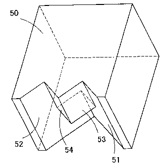
Fig. 8 is a perspective view showing a shape of the mirror
block 50 which is fixed to the end portion of the iron piece
40, and Fig. 9 (a) , (b) are a plan view and a front view of the
mirror block 50. The mirror block 50 is made of metal, glass,
plastic or the like and is formed in a substantially rectangular
parallelepiped shape. On a left side and a right side of a
front surface of the mirror block 50, a first light reflection
surface 51 and a second light reflection surface 52 are formed
in a state that both reflection surfaces 51, 52 make an angle
of 90 degree therebetween. Further, on a left side and a right
side of an upper half portion of the front surface of the mirror
block 50, a third light reflection surface 53 and a fourth light
reflection surface 54 are formed in a projecting manner in a
state that both reflection surfaces 53, 54 make an angle of
90 degree therebetween. Here, the third light reflection
surface 53 and the first light reflection surface 51 also make
an angle of 90 degree therebetween, while the fourth light
reflection surface 54 and the second light reflection surface
52 also make an angle of 90 degree therebetween. Accordingly,
on the upper half portion of the front surface of the mirror
block 50, the first light reflection surface 51, the third light
reflection surface 53, the second light reflection surface 52
and the fourth light reflection surface 54 are formed in a
18
CA 02488054 2004-12-O1
W-groove shape in a state that these reflection surfaces make
an angle of 90 degrees from each other, while on the lower half
portion of the front surface of the mirror block 50, the first
light reflection surface 51 and the second light reflection
surface 52 are formed in a V-groove shape in a state that these
surfaces 51, 52 also make an angle of 90 degree therebetween.
To be more specific, on the upper half portion of the mirror
block 50, the first light reflection surface 51 as well as the
third light reflection surface 53 and the second light reflection
surface 52 as well as the fourth light reflection surface 54
are arranged in a face symmetry with respect to a center plane,
while on the lower half portion of the mirror block 50, the
first light reflection surface 51 and the second light reflection
surface 52 are arranged in a face symmetry with respect to a
center plane.
The mirror block 50 has a lower surface thereof fixed
to an upper surface of an end portion of the iron piece 40 using
an adhesive agent, wherein the light reflection surfaces 51,
52, 53 and 54 formed in a W-groove shape are arranged on the
mirror block 50 and the light reflection surfaces 51, 52 formed
in a V-groove shape are arranged below the mirror block 50.
Opposite to such a structure, it may be possible to bond the
iron piece 40 in a state that the upper surface of the mirror
block 50 is directed downwardly so as to arrange the light
reflection surfaces 51, 52 formed in a V-groove shape on the
19
CA 02488054 2004-12-O1
mirror block 50 and to arrange the light reflection surfaces
51, 52, 53 and 54 formed in a W-groove shape below the mirror
block. However, in such a structure, at the time of performing
the bonding operation of the mirror block 50, an adhesive agent
rises from the V groove formed between the first light reflection
surface 51 and the third light reflection surface 53 and the
V groove formed between the fourth light reflection surface
54 and the second light reflection surface 52 due to a capillarity
and is liable to easily smear the light reflection surfaces.
In this embodiment, by adhering the mirror block 50 to the iron
piece 40 with the lower surface of the mirror block 50 directed
downwardly, the adhesive agent rises through only one V groove
which is formed between the first light reflection surface 51
and the second light reflection surface 52 and hence, the light
reflection surfaces are hardly smeared with the adhesive agent.
The optical fiber installation unit 26 is constituted
of a support base 55 which is formed in an approximately U shape
shown in Fig . 10 and an adj us table plate 56 shown in Fig . 11 .
The support base 55 is provided with recessed portions 58 on
upper surfaces of both side portions thereof and has a bottom
surface thereof preliminarily fixed to an upper surface of the
board 24. Rod-like arms 57 extend from both side surfaces of
the adjustment plate 56. The adjustment plate 56 is fixed to
a lower surface of an optical fiber array 27 using an adhesive
agent before beingmounted on the support base 55. Subsequently,
CA 02488054 2004-12-O1
the arms 57 of the adjustment plate 56 on which the optical
fiber array 27 is mounted are accommodated in the recessed
portions 58 of the support base 55, the position of the optical
fiber array 27 is adjusted and, thereafter, the arms 57 are
fixed to the inside of the recessed portions 58 using an adhesive
agent, and the optical fiber array 27 is supported in the air
by the adjustment plate 56.
Fig. 12 is an exploded perspective view of the optical
fiber array 27. In the optical fiber array 27, end portions
of four optical fibers 32, 33, 34 and 35 are held in the inside
of a holder 59 . The distal end portions of the respective optical
fibers 32, 33, 34 and 35 have axes thereof finely positioned
in the inside of the holder 59 and are arranged in parallel
to each other in a row with a given pitch, and are fixed in
such a state. To be more specific, the first input optical
fiber 32, the first output optical fiber 34, the second input
optical fiber 33, and the second output optical fiber 35 are
sequentially arranged. As means for finely positioning the
optical fibers 32, 33, 34 and 35 in the holder 59, the optical
fibers 32, 33, 34 and 35 may be fitted into a multi-core ferrule
or the optical fibers 32, 33, 34 and 35 may be fitted into a
V-shaped groove. Further, a lens array 60 is fixed to a front
surface of the holder 59 using an adhesive agent or the like.
On the lens array 60, minute coupling lenses 61 are formed in
a state that the coupling lenses 61 face respective end surfaces
21
CA 02488054 2004-12-O1
of the optical fibers 32, 33, 34 and 35. As this lens array
60, the coupling lenses 61 made of transparent resin may be
formed on a transparent resin board, or the coupling lenses
61 made of glass may be formed on a glass board, or the coupling
lenses 61 made of glass may be formed on a transparent resin
board, or the coupling lenses 61 made of transparent resin may
be formed on a glass board. The lens array 60 is arranged in
front of the holder 59 with an uncured adhesive agent
therebetween and, thereafter, lights are radiated to the
respective coupling lenses 61 from the respective optical fibers
32, 33, 34 and 35, and the lights which pass through the respective
coupling lenses 61 are monitored thus aligning the optical axes
of the optical fibers 32, 33, 34 and 35 and the axes of the
coupling lenses 61, and the adhesive agent is cured in such
a state so as to fix the lens array 60 to the front surface
of the holder 59.
Next, the assembling step of the optical switch 21 is
explained. In the assembling step of the optical switch 21,
first of all, the mirror unit 25 is mounted on the board 24
by soldering the lead legs 69 of the mirror unit 25 to electrode
pads 30 of the board 24. The mirror block 50 is preliminarily
mounted on the mirror unit 25 . The support base 55 of the optical
fiber installation unit 26 is also arranged at a position which
faces the mirror unit 25 in an opposed manner and is adhered
to an upper surface of the board 24 preliminarily.
22
CA 02488054 2004-12-O1
Next, as shown in Fig. 11, the adjustment plate 56 is
adhered to the lower surface of the optical fiber array 27 so
as to integrate the optical fiber array 27 and the adjustment
plate 56. The optical fiber array 27 is gripped by a robot
hand and is transported to a position above the support base
55 and arms 57 of the adjustment plate 56 which are fixed to
the lower surface of the optical fiber array 27 are accommodated
in the inside of the recessed portions 58 formed in the support
base 55.
Thereafter, the mirror block 50 is elevated so as to make
the first light reflection surface 51 and the second light
reflection surface 52 face the optical fibers 32, 33, 34 and
35 in an opposed manner. In such a state, the optical fiber
array 27 is moved to perform the adjustment of the optical axis
positions (see Fig. 13 (b) ) and the position of the optical fiber
array 27 is stored in the computer. Next, the mirror block
50 is lowered to make the first light reflection surface 51,
the third light reflection surface 53, the fourth light
reflection surface 54 and the second light reflection surface
52 face the optical fibers 32, 33, 34 and 35 in an opposed manner.
In such a state, the optical fiber array 27 is moved to perform
the adjustment of optical axes positions (see Fig. 13 (a) ) , and
the position of the optical fiber array 27 is stored in the
computer. In this manner, by detecting the optical axes
adjustment positions of the optical fiber array 27 in the state
23
CA 02488054 2004-12-O1
that the mirror block 50 is elevated and in the state that the
mirror block 50 is lowered and by making the computer store
the respective positions, the computer calculates an optimum
position based on the data (for example, an average position
of both positions being obtained). When the optimum position
of the optical fiber array 27 is calculated by the computer,
the optical fiber array 27 is finely adjusted by the robot hand
to assume the optimum position and is held in such a state.
While holding this state, an ultraviolet ray curing type adhesive
agent is dropped between the arms 57 and the recessed portions
58 and the ultraviolet ray curing type adhesive agent is cured
by radiating ultraviolet rays to the ultraviolet ray curing
type adhesive agent thus fixing the arms 57 in the inside of
the recessed portions 58 using an adhesive agent whereby the
optical fiber array 27 is eventually fixed to the final
adjustment position. Here, provided that a fast curing type
adhesive agent is used as the adhesive agent which serves to
fix the arms 57, the adhesive agent is not limited to the
ultraviolet ray curing type adhesive agent. Further, the arms
57 may be fixed using soldering or the like in place of the
adhesive agent.
By mounting the mirror unit 25 and the optical fiber
installation unit 26 in the inside of the board 24, the optical
switch body 22 is assembled. In this optical switch body 22,
the mirror block 50 of the mirror unit 25 and the end surfaces
24
CA 02488054 2004-12-O1
of the respective optical fibers 32, 33, 34 and 35 of the optical
fiber array 27 face each other, and when the electromagnet 38
of the mirror unit 25 is energized and an end portion of the
iron piece 40 on a side opposite to a side on which the mirror
block 50 is formed is attracted, the mirror block 50 is elevated.
In this state, the third light reflection surface 53 and the
fourth light reflection surface 54 are elevated higher than
a plane which includes the axes of end portions of the optical
fibers 32, 33, 34 and 35. Accordingly, as shown in Fig. 13 (b) ,
in the lower half portion of the mirror block 50, the first
input optical fiber 32 and the first output optical fiber 34
face the first light reflection surface 51 and the second input
optical fiber 33 and the second output optical fiber 35 face
the second light reflection surface 52. Further, when the
electromagnet 38 of the mirror unit 25 is energized and an end
portion on the side on which the mirror block 50 of the iron
piece 40 is formed is attracted, the mirror block 50 is lowered
downwardly. In this state, as show in Fig. 13 (a) , in the upper
half portion of the mirror block 50, the first input optical
fiber 32 faces the first light reflection surface 51 in an opposed
manner and the first output optical fiber 34 faces the third
light reflection surface 53 in an opposed manner, the second
input optical fiber 33 faces the fourth light reflection surface
54 in an opposed manner, and the second output optical fiber
35 faces the second light reflection surface 52 in an opposed
CA 02488054 2004-12-O1
manner.
Here, assuming that the positional relationship between
the respective optical fibers 32, 33, 34 and 35 and the respective
light reflection surfaces 51, 52, 53 and 54 is accurately
adj usted, with respect to the optical switch 21 in the changeover
state in which the mirror block 50 is lowered as shown in Fig.
13 (a) , a light 66 which is radiated from the first input optical
fiber 32 is reflected on the first light reflection surface
51 and the third light reflection surface 53 and, thereafter,
is incident on the first output optical fiber 34. Further,
a light 67 which is radiated from the second input optical fiber
33 is reflected on the fourth light reflection surface 54 and
the second light reflection surface 52 and, thereafter, is
incident on the second output optical fiber 35. Accordingly,
in such a changeover state, the first input optical fiber 32
and the first output optical fiber 34 are coupled, while the
second input optical fiber 33 and the second output optical
fiber 35 are coupled.
To the contrary, with respect to the optical switch 21
in the changeover state in which the mirror block 50 is elevated
as shown in Fig. 13(b), the light 66 which is radiated from
the first input optical fiber 32 is reflected on the first light
reflection surface 51 and the second light reflection surface
52 and, thereafter, is incident on the second output optical
fiber 35. Further, the light 67 which is radiated from the
26
CA 02488054 2004-12-O1
second input optical fiber 33 is reflected on the second light
reflection surface 52 and the first light reflection surface
51 and, thereafter, is incident on the first output optical
fiber 34. Accordingly, in such a changeover state, the first
input optical fiber 32 and the second output optical fiber 35
are coupled, while the second input optical fiber 33 and the
first output optical fiber 34 are coupled.
Here, even when the positions of the mirror block 50 and
the optical fiber array 27 are finely adjusted, there may arise
a case in which the arms 57 are moved until the adhesive agent
is completely cured and hence, the positional adjustment is
again required after mounting the optical fiber array 27. To
cope with such a case, as shown in Fig. 14, the arms 57 are
formed in a bent shape or in a zigzag shape and hence, even
after the adjustment plate 56 is fixed to the support base 55,
the arms 57 are plastically deformed thus moving the optical
fiber array 27 together with the adjustment plate 56 so as to
perform the positional adjustment of the optical fiber array
27 in the longitudinal direction as well as in the lateral
direction. Alternatively, an angle of the optical fiber array
27 may be adjusted.
When the positional adjustment of the optical fiber array
27 is completed, the upper surface of the optical switch body
22 is covered with a cover 23 so as to seal an upper surface
of the optical switch body 22. Due to such a constitution,
27
CA 02488054 2004-12-O1
it is possible to manufacture the optical switch 21 having the
sealing structure.
(Second Embodiment)
Fig. 15(a), (b) and (c) are a plan view, a front view
and a lower plan view with a part broken away showing the structure
of a mirror block 50 used in the optical switch according to
the second embodiment of the invention. In the first mirror
block 50, with respect to a V groove formed between the first
light reflection surface 51 and the second light reflection
surface 52, a V groove formed between the first light reflection
surface 51 and the third light reflection surface 53, and a
V groove formed between the fourth light reflection surface
54 and the second light reflection surface 52, by embedding
the deepest portions of the respective V grooves, flat surface
portions 62, 63, 63 are formed thus making the suction of the
adhesive agent even at the deep portions of the V grooves due
to the capillarity difficult at the time of adhering the mirror
block 50. Although the deep portions of the V grooves are made
flat in the drawing, there is no problem in forming the portions
of the V grooves into a curved surface. In this manner, by
setting a lower limit value with respect to a groove width at
the deep portions of the V grooves, it is possible to make the
suction of the adhesive agent to the light reflection surfaces
difficult and hence, the light reflection surfaces are further
hardly smeared with the adhesive agent.
28
CA 02488054 2004-12-O1
Here, in this embodiment, an opening width W1 of the V
groove formed between the first light reflection surface 51
and the second light reflection surface 52 is set to 1mm,
respective opening widths W2 of the V groove formed between
the first light reflection surface 51 and the third light
reflection surface 53 and the V groove formed between the fourth
light reflection surface 54 and the second light reflection
surface 52 are set to 0.5mm, and a width W3 of the flat surface
portions 62, 63 of the deep portions of the V grooves is set
to substantially 50Eun.
(Third embodiment)
In the mirror unit 25 having the above-mentioned structure,
since the mirror block 50 is elevated or lowered by rotating
the iron piece 40 like a seesaw, an angle of the front surface
(light reflection surface) of the mirror block 50 is changed
vertically between when the mirror block 50 is elevated and
when the mirror block 50 is lowered. Particularly, when the
mirror unit 25 is miniaturized, the change of the angle when
the mirror block 50 is elevated or lowered is increased and
hence, there exists a possibility that the lights which are
radiated from the input optical fibers 32, 33 and are reflected
on the mirror block 50 are deviated from the output optical
fibers 34, 35. In such a case, the mirror block 50 having the
structure shown in Fig. 16 and Fig. 17 (a) , (b) , (c) may be used.
Fig. 16 is a perspective view showing the structure of
29
CA 02488054 2004-12-O1
the mirror block 50 used in the optical switch according to
the third embodiment of the invention. Fig. 17(a) is a plan
view of the mirror block 50 and Fig. 17 (b) , (c) are respectively
a cross-sectional view taken along a line X-X in Fig. 17(a)
and a cross-sectional view taken along a line Y-Y in Fig. 17 (a) .
With respect to this mirror block 50, a lower half of the front
surface of the mirror block 50 is formed in a V-groove shape
by a first light reflection surface 51a and a second light
reflection surface 52a and, at the same time, the first light
reflection surface 51a and the second light reflection surface
52a are inclined downwardly such that normal lines which are
erected from the first light reflection surface 51a and the
second light reflection surface 52 are included in the same
plane as optical axes of distal ends of the optical fibers 32,
33, 34 and 35 when a mirror block 50 mounted on a mirror unit
25 is elevated. Further, an upper half of the front surface
of the mirror block 50 is formed into a W-groove shape due to
a first light reflection surface 51b, a second light reflection
surface 52b, a third light reflection surface 53, and a fourth
light reflection surface 54 and, at the same time, the first
light reflection surface 51b, the second light reflection
surface 52b, the third light reflection surface 53, and the
fourth light reflection surface 54 are inclined upwardly such
that normal lines which are erected from the first light
reflection surface 51b, the second light reflection surface
CA 02488054 2004-12-O1
52b, the third light reflection surface 53, and the fourth light
reflection surface 54 are included in the same plane as the
optical axes of distal ends of the optical fibers 32, 33, 34
and 35 when the mirror block 50 mounted on the mirror unit 25
is lowered.
Accordingly, using such a mirror block 50, there is no
possibility that the lights reflected on the mirror block 50
are deviated from the plane which includes the optical axes
of the optical fibers 32, 33, 34 and 35 whereby the alignment
of the axes of the respective first light reflection surfaces
51a, 51b, 52a, 52b, 53 and 54 and the axes of the respective
optical fibers 32, 33, 34 and 35 can be easily performed and,
at the same time, the coupling efficiency of the optical switch
21 can be enhanced.
(Fourth Embodiment)
The embodiment shown in Fig. 18 is directed to a 1x2 type
optical switch which includes one input optical fiber and two
output optical fibers . In this embodiment, when a mirror block
50 is lowered, a first output optical fiber 34 faces a third
light reflection surface 53 in an opposed manner, an input
optical fiber 64 faces a fourth light reflection surface 54
in an opposed manner, and a second output optical fiber 35 faces
a second light reflection surface 52 in an opposed manner.
Here, in the optical switch having such a constitution,
in a changeover state in which the mirror block 50 is lowered,
31
CA 02488054 2004-12-O1
as shown in Fig. 18(a), a light 65 which is radiated from an
input optical fiber 64 is reflected on a fourth light reflection
surface 54 and a second light reflection surface 52 and,
thereafter, is incident on a second output optical fiber 35.
Accordingly, in this changeover state, the input optical fiber
64 and the second output optical fiber 35 are coupled to each
other.
On the other hand, in a changeover state in which the
mirror block 50 is elevated, as shown in Fig. 18(b), a light
65 which is radiated from an input optical fiber 64 is reflected
on a second light reflection surface 52 and a first light
reflection surface 51 and, thereafter, is incident on a first
output opticalfiber34. Accordingly, in thischangeoverstate,
the input optical fiber 64 and the first output optical fiber
34 are coupled to each other.
Here, it is possible to apply this embodiment to a 1x2
type optical switch which includes two input optical fibers
and one output optical fiber.
(Fifth embodiment)
The embodiment shown in Fig. 19 is directed to a 4x4 type
optical switch which includes four input optical fibers and
tour output optical fibers. In this optical switch, when a
mirror block 50 is lowered, a first input optical fiber 71 and
a second input optical fiber 72 are arranged to face a first
light reflection surface 51 in an opposed manner, a first output
32
CA 02488054 2004-12-O1
optical fiber 75 and a second output optical fiber 7 6 are arranged
to face a third light reflection surface 53 in an opposed manner,
a third input optical fiber 73 and a fourth input optical fiber
74 are arranged to face a fourth light reflection surface 54
in an opposed manner, and a third output optical fiber 77 and
a fourth output optical fiber 78 are arranged to face a second
light reflection surface 52 in an opposed manner.
Here, in a changeover state in which the mirror block
50 is lowered, lights 79, 80 which are radiated from the first
input optical fiber 71 and the second input optical fiber 72
are reflected on the first light reflection surface 51 and the
third light reflection surface 53 and, thereafter, are
respectively incident on the second output optical fiber 76
and the first output optical fiber 75 . Further, lights 81, 82
which are radiated from the third input optical fiber 73 and
the fourth input optical fiber 74 are reflected on the fourth
light reflection surface 54 and the second light reflection
surface 52 and, thereafter, are respectively incident on the
fourth output optical fiber 78 and the third output optical
fiber 77 . Accordingly, in this changeover state, the first input
optical fiber 71 and the second output optical fiber 76 are
coupled to each other, the second input optical fiber 72 and
the first output optical fiber 75 are coupled to each other,
the third input optical fiber 73 and the fourth output optical
fiber 78 are coupled to each other, and the fourth input optical
33
CA 02488054 2004-12-O1
fiber 74 and the third output optical fiber 77 are coupled to
each other.
On the other hand, in a changeover state in which the
mirror block 50 is elevated, as shown in Fig. 19(b), lights
79,80 which are radiated from the first input optical fiber
71 and the second input optical fiber 72 are reflected on the
first light reflection surface 51 and the second light reflection
surface 52 and, thereafter, are respectively incident on the
fourth output optical fiber 78 and the third output optical
fiber 77. Further, lights 81,82 which are radiated from the
third input optical fiber 73 and the fourth input optical fiber
74 are reflected on the second light reflection surface 52 and
the first light reflection surface 51 and, thereafter, are
respectively incident on the second output optical fiber 76
and the first output optical fiber 75. Accordingly, in this
changeover state, the first input optical fiber 71 and the fourth
output optical fiber 78 are coupled to each other, the second
input optical fiber 72 and the third output optical fiber 77
are coupled to each other, the third input optical fiber 73
and the second output optical fiber 76 are coupled to each other,
and the fourth input optical fiber 74 and the first output optical
fiber 75 are coupled to each other.
(Sixth embodiment)
When the mirror block 50 shown in the first embodiment
is used, as can be understood from Fig. 13 (a) (b) , for example,
34
CA 02488054 2004-12-O1
between the case in which the light 66 which is radiated from
the first input optical fiber 32 is reflected on the first light
reflection surface 51 and the third light reflection surface
53 and is incident on the first output optical fiber 34 and
the case in which the light 66 which is radiated from the first
input optical fiber 32 is reflected on the first light reflection
surface 51 and the second light reflection surface 52 and is
incident on the second output optical fiber 35, the spatial
optical path ranging from the radiation of the light 66 from
the first light reflection surface 51 to the inputting of light
into the first output optical fiber 34 and the spatial optical
path ranging from the radiation of the light 66 from the first
light reflection surface 51 to the inputting of light 66 into
the second output optical fiber 35 differ from each other.
Accordingly, the light 66 which is incident on the first output
optical fiber 34 and the light 66 which is incident on the second
output optical fiber 35 differ in a phase and a diameter of
light spot thereof at end surfaces of the fibers. Accordingly,
when the optical switch is changed over, the characteristics
of an optical signal are changed and hence, there exists a
possibility that it is necessary to perform the adjustment of
the lens positions or the coupling efficiencies are changed.
Fig. 20 is a perspective view showing the structure of
a mirror block 50 which is optimum for overcoming the
above-mentioned drawback. In this mirror block 50, a lower
CA 02488054 2004-12-O1
half of a front surface of the mirror block 50 is formed in
a V-groove shape due to a first light reflection surface 51a
and a second light reflection surface 52a, while an upper half
of a front surface of the mirror block 50 is formed in a W-groove
shape due to a first light reflection surface 51b, a second
light reflection surface 52b, a third light reflection surface
53 and a fourth light reflection surface 54 . Further, the first
light reflection surface 51b, the second light reflection
surface 52b, the third light reflection surface 53 and the fourth
light reflection surface 54 which are formed on the upper half
are retracted backwardly than the first light reflection surface
51a and the second light reflection surface 52a which are formed
on the lower half and hence, even when either one of the upper
portion and the lower portion is used, the spatial optical path
length is not changed.
Fig. 21 (a) , (b) show the state in which the mirror block
50 is lowered and the first light reflection surface 51b, the
second light reflection surface 52b, the third light reflection
surface 53 and the fourth light reflection surface 54 are used
and the state in which the mirror block 50 is elevated and the
first light reflection surface 51a and the second light
reflection surface 52a are used. As can be understood from
the geometric relationship between the optical paths for the
light 66 and the light 67 shown in Fig. 13 (a) , (b) , the distance
that the spatial optical path length is elongated when the state
36
CA 02488054 2004-12-O1
of the optical switch is changed from the state shown in Fig.
13 (a) to Fig. 13 (b) is equal with respect to both of the light
66 and the light 67 . Accordingly, by retracting the first light
reflection surface 51b, the second light reflection surface
52b, the third light reflection surface 53 and the fourth light
reflection surface 54 backwardly by a half of this distance,
it is possible to prevent the change of the spatial optical
path length.
According to this embodiment, the adjustment of the lens
positions or the like which is required along with the changeover
of the optical switch becomes no more necessary and the change
of the coupling rate of light can be prevented.
Here, in the above-mentioned embodiments, although the
driven portion 39 of the mirror unit 25 is driven like a seesaw
to rotate the mirror block 50, the mirror block 50 may be moved
in parallel in the vertical direction by elevating or lowering
the driven portion 39. Further, the mirror unit 25 moves the
mirror block 50 using the electromagnet, the mirror unit 25
may move the mirror block 50 using other method such as an
electrostatic actuator, a voice coil or the like. Further,
even when the electromagnet is used, it may be possible that
only one electromagnet is used, wherein the mirror block 50
assumes the lowered position when the electromagnet is energized
and assumes the elevated position when the electromagnet is
deenergized. Further, even when the electromagnet is used,
37
CA 02488054 2004-12-O1
there exists no problem in using the electromagnet of a type
which is not latched.
Industrial Applicability
As has been explained heretofore, the invention provides
the optical switch for changing over the optical fiber
transmission path or thelight transmission/reception terminal
used in the optical communication and the optical switch is
used at the coupling portion between the input optical path
(for example, the input optical fiber) and the output optical
path (for example, the output optical fiber).
38