Note: Descriptions are shown in the official language in which they were submitted.
CA 02488263 2004-12-O1
WO 03/102648 PCT/DK03/00367
AN OPTICAL COMPONENT AND A METHOD OF FABRICATING AN
OPTICAL COMPONENT
TECHNICAL FIELD
The present invention relates to the field of planar optical components for
use
in optical communications systems.
The invention relates specifically to a method of manufacturing an optical
component.
It also relates to a branching unit and to a method of reducing insertion loss
in an optical branching unit.
It further relates to a method of reducing stress induced polarization effects
in
spaced planar waveguides (e.g. couplers) and stress induced tilting of the
cores due to strain fields introduced by the top-cladding.
It also relates to a method for filling high-aspect-ratio structures with
material
during reflow.
The invention may e.g. be useful in applications such as optical
communications systems, specifically in connection with the distribution of
signals in optical systems (e.g. CATV) or components, e.g. in the form of low
~25 loss, high uniformity splitters, couplers and variable optical attenuators
(VOAs), either as individual components or integrated with other functions on
a chip.
BACKGROUND ART
The following account of the prior art relates to one of the areas of
application
of the present invention, optical communications systems.
CA 02488263 2004-12-O1
WO 03/102648 PCT/DK03/00367
2
Loss reduction:
A planar optical branching component, such as a power Y-splitter, often plays
a fundamental role in simple as well as complicated designs. The function
that a Y-splitter performs is to divide the incoming signal into typically two
signals of equal magnitude (50%:50%). It should be noted, that even though
we in this text focus on the so-called Y-splitters, the presented idea can be
used in branching components that divide the incoming signals) into more
than just two output waveguides as well as into varying splitting ratios, not
just 50%:50%.
Often it is of interest to be able to divide one or more signals into a large
number of signals. To achieve this goal typically a so-called splitter tree is
used where a number of fundamental splitters are concatenated. A 1-4
splitter (tree) is then realized by concatenating two 1-2 splitters to the two
outputs of a first 1-2 splitter. Furthermore, a 1-8 splitter is realized by
concatenating four 1-2 splitters to the 1-4 splitter (one 1-2 splitter to each
of
the four outputs). In this way it is possible to realize 1-2N splitter-trees
using
only the simple 1-2 splitter. 2-2N can be realized using a similar approach
where a 2-2 branching component (e.g. a coupler) is followed by two
separate 1-2N-~ splitter trees.
Typically it is desirable that the splitter distributes the incoming signal
equally
between the output waveguides and with minimum optical loss. To achieve
the goal of equal splitting, the individual splitters need to divide the
incoming
signals equally, i.e. x%:x% where x is as close as possible to 50.
If a splitter divides the signal equally and without loss, i.e. x = 50, the
intensity of the signal in the two output waveguides will be P°utpUt = -
10*log('/2)
= 3.01 dB lower than the original signal. For a loss-less 1-4 splitter the
power
in the four output waveguides will be P°~tp~t = 2*3.01 = 6.02 dB lower
than the
original signal, and for a 1-16 splitter the output power will be
P°utput = 4*3.01
= 12.04 dB than the original signal. Thus for a 1-16 splitter the theoretical
minimum reduction in the power level in an equally splitting component will
be 12.04 dB.
CA 02488263 2004-12-O1
WO 03/102648 PCT/DK03/00367
3
There is no such thing as a loss-less passive optical components since there
will always be coupling losses, propagation losses, radiation losses etc.
These loss factors can be minimized by proper choice of waveguide cross-
sectional geometry, refractive index of the core material and cladding
materials, as well as by choosing suitable curve-forms for the component
layout. By suitable choices we managed to fabricate low-loss 1-16
components having typical values of insertion loss in the neighbourhood of
13.5 dB which is 13.5 - 12.04 = 1.46 dB above the theoretical minimum.
Assuming that the extra loss is equally distributed among the four splittings
in
the 1-16 splitter tree the loss per fundamental splitter is 1.46 dB/4 = 0.365
dB
(neglecting the coupling loss from the fibre to the chip). In order to come
near
the theoretical minimum we thus need to reduce the excess loss per splitter
by a few tenths of a dB.
US-A-5,745,618 discloses a 1-P power splitter comprising an input
waveguide and P output waveguides that are all coupled to a slab waveguide
in the form of a planar area, which is large compared to the area of an
individual waveguide and designed to support light wave transmission
between the input and output waveguides. The power splitter further
comprises a transition region immediately adjacent to the slab waveguide
which comprises a number of silica paths (e.g. 30) that transversely intersect
the output waveguides. The silica paths are generally parallel to each other
and have widths that progressively decrease as they become further away
from the slab waveguide.
The present application discloses an optical branching component and a
method of reducing the loss of optical power in branching components, in
particular 1-2N splitters, which makes possible the fabrication of e.g. 1-16
(N=4) splitters having an insertion loss of approximately 12.3 - 12.5 dB
(typically).
Stress relieving:
The present invention further deals with the issue of reducing stress induced
polarization effects and stress induced tilting of the cores in planar optical
CA 02488263 2004-12-O1
WO 03/102648 PCT/DK03/00367
4
components, e.g. waveguide couplers. Since the top-cladding introduces a
non-symmetric strain field across closely spaced waveguides, measures
have to be taken to minimize these effects.
One way to reduce this non-symmetric behaviour is to place the waveguide
cores of the coupler as far apart as possible to approach an isolated
waveguide situation. This way each waveguide core in the coupler will see a
quasi-symmetrical surrounding and the strain field will be more uniform
across the waveguide core. By placing the waveguide cores far apart in the
coupler region, the length of the coupler device will be significantly
larger..
Therefore this solution is not very suitable for compact device design.
Other means of reducing this effect is by using a polymer over-cladding that
is heat-treated at low temperatures (< 300°C). Because of the
relatively low
process temperature, the thermally induced stress effects will be smaller and
consequently the stress levels lower. Polymer top-cladding has an inherent
reliability problem and is therefore generally not used in commercial
products.
Gap-filling:
The present invention further deals with the issue of gap-filling, which for
planar waveguide fabrication is a technological challenge. Since most of the
deposition processes are of a planar type, special measures have to be
taken to fill high-aspect-ratio trenches (e.g. trenches that have a height to
width ratio larger than 2 where the height dimension is taken in a direction
of
growth of the planar process and the width dimension is taken perpendicular
thereto). This can ~be done by adding e.g. boron and phosphorus to the glass
whereby the flowing temperature can be reduced to typical anneal
temperatures used in planar waveguide fabrication. The reflow-properties of
the glass is, however, very dependent on the structures that have to be
covered, e.g. a directional coupler. A directional coupler may be used either
as an .individual component in itself, or as a part in a larger functionality.
A
directional coupler consists of two separate waveguides which, over a
distance known as the coupling length (LcR), are closely spaced (cf. FIG. 21
).
CA 02488263 2004-12-O1
WO 03/102648 PCT/DK03/00367
If the two cores pertaining to the two separate waveguides are sufficiently
close, the exponentially decaying tail of the optical field in the first
waveguide
core may be able to reach into the core of the second waveguide core. Being
in the second waveguide core, the field pertaining to the first waveguide core
5 is creating a polarization of the atoms in the core medium which in turn
generates a new optical field in the second core. The greater the magnitude
of the field pertaining to waveguide 1 in waveguide 2, the greater is the
polarization and hence the faster the transfer of energy, which translates to
a
shorter length for full coupling. In this way the energy in the field in .the
first
waveguide core can be gradually transferred to the second waveguide core.
As the field decays exponentially outside the core regions of either of the
waveguides, it is necessary that the two waveguide cores are closely spaced
if good coupling and hence a short coupling length is to be achieved. If the
distance between the two waveguide cores increases, the distance along the
length in which a certain percentage of the energy from the field in the first
waveguide is coupled to the field in the second waveguide increases
exponentially. The smaller the components, the more components per unit
area or wafer may be implemented, which - for directional couplers - requires
that the waveguide cores in the coupling region be closely spaced.
In a directional coupler where the two cores are closely spaced, the distance
edge-to-edge between the two cores is small (e.g. less than 5 pm apart or
even less than 1 Nm apart), especially relative to the waveguide height - i.e.
there will be a large aspect-ratio (waveguide height divided by the edge-to
edge distance).
In a deposit-etch-deposit planar technology, a layer of core material is
firstly
deposited on a lower cladding layer, secondly the core layer is patterned
using standard photolithographic techniques and the pattern is transferred to
the core layer by etching. The pattern created during the etch step is finally
covered and protected by deposition of a layer of material typically having
optical characteristics as the lower cladding layer.
If one uses a deposition method that does not deposit conformably onto the
underlying structures, i.e. does not deposit as fast (typically slower) on
vertical faces (in a direction of growth or deposition) as on horizontal faces
CA 02488263 2004-12-O1
WO 03/102648 PCT/DK03/00367
6
(i.e. parallel to a planar face of the substrate and perpendicular to a
direction
of growth of planar layers), problems are likely to arise in areas having
large
aspect-ratios. During deposition the area above the narrow opening will
gradually close while leaving the volume between the two waveguides partly
empty (i.e. comprising voids, so-called 'keyholes' or 'air-pockets'). The
deposition rate at the horizontal face at the bottom of the narrow opening is
considerably lower than on horizontal faces outside the coupling region, as
the material flow into the volume between the two waveguides is restricted by
a shadowing effect from the waveguides themselves. Furthermore, the
deposition of material grows laterally (i.e. extending from side to side) from
the upper corners of the waveguides towards the central part of the coupling
region which further increases the shadowing effect. The result is that a void
or air pocket is created in the region between the two waveguides (cf. FIG.
22.b).
The magnitude of the exponentially decaying evanescent field tail is more or
less exponentially dependent upon the refractive index difference of the core
material and the surrounding material. Typically the refractive index of the
material that surrounds the core will have a value only slightly smaller than
that of the core, in order to create a structure that is matched to a standard
optical fibre, e.g. a SMF-28 fibre. For such a fibre the core refractive index
typically is around 1.450 @ 1.55 Nm, whereas the cladding refractive index
has a refractive index around 1.445 @ 1.55 pm, i.e. a refractive index
difference of around 5~10-3. If a void is present between the two closely
spaced waveguide cores of the directional coupler this void will constitute an
area having a refractive index 1 (that of a vacuum), hence the refractive
index difference will now be around 0.450. This will obviously make the
optical coupling between the two waveguides uncontrollable and non-
reproducible and thus render the component useless.
To ease the filling of the narrow space between the two waveguides in the
coupling region, a multi-step process is typically applied. In such a process
a
layer of cladding material is deposited followed by a high-temperature
treatment where the entire structure is heated to above the glass-transition
temperature of the cladding material, which makes the cladding material soft.
When the cladding material is soft it can flow and redistribute itself
(reflow)
CA 02488263 2004-12-O1
WO 03/102648 PCT/DK03/00367
7
thereby better fill the narrow spaces. This process is repeated a number of
times making it possible to cover most encountered structures. However,
sometimes structures/designs having aspect-ratios that prevent perfect filling
of the narrow spaces are seen.
One solution to the problem of gap filling is to increase the doping level of
boron and phosphorus. This will "soften" the cladding material even further
and thereby promoting the gap filling. However, the higher doping
concentration makes the glass less reliable and more susceptible to water. It
is therefore necessary to use hermetical packaging which increases the cost
of the components.
Another solution to the problem is to use other deposition processes such as
flame-hydrolysis deposition (FHD) or Low Pressure Chemical Vapour
Deposition (LPCVD). Both these processes have better step-coverage
properties than plasma enhanced chemical vapour deposition (PECVD), but
other factors such as lack of scalability, flexibility, control and automatic
fabrication, etc. speak against these methods.
DISCLOSURE OF INVENTION
The present invention proposes the use of additional structural elements
such as transversal elements connected to or pads or elongate elements
located in the vicinity of ordinary waveguide core sections. The additional
structural elements are typically formed in the same processing step as the
ordinary waveguide core sections. The additional structural elements have
the purpose of enabling (an experimentally observed fact of) a better filling
of
small volumes between closely spaced waveguide core sections with
cladding material thereby avoiding the creation of voids and to reduce the
stress induced in neighbouring waveguide core sections thereby reducing
birefringence. In some cases this or these effects may be combined with an
improved control of the coupling of light from one waveguide to the other
(such as in a directional coupler) or the provision of a gradual change in
refractive index over a certain length between neighbouring waveguides
(such as in a splitter), thereby reducing insertion loss.
CA 02488263 2004-12-O1
WO 03/102648 PCT/DK03/00367
A method of manufacturingi an optical component comprisingi transversal
elements:
Objects of the invention are achieved by a method of manufacturing an
optical component comprising a combination of planar waveguides on a
substrate, the combination of waveguides comprising spaced, parallel,
diverging or merging waveguide core sections forming a core region layout in
a planar view, the method comprising the steps of
a) providing a substrate,
b) forming a lower cladding layer on the substrate,
c) forming a core layer on the lower cladding layer,
d) providing a core mask comprising a core pattern corresponding to the core
region layout and a layout of transversal elements, the transversal elements
extending between at least two of said spaced, parallel, diverging or merging
waveguide core sections, thereby fully or partially connecting them,
e) forming core sections and transversal elements using said core mask, a
photolithographic and an etching process, and
f) forming an upper cladding layer to cover the waveguide core sections, the
transversal elements and the lower cladding layer
wherein at least one of the steps b), c), f) is performed by plasma enhanced
chemical vapour deposition.
Advantages of the invention are that a combined effect of preventing or
minimizing the generation of voids in the cladding layer around closely
spaced waveguide core sections and the precise control of the refractive
index in the region between spaced waveguides, potentially leading to lower
losses of the component. The use of plasma enhanced chemical vapour
deposition (PECVD) in the manufacturing process has the advantages of a
commercially available, proven technology from many years of service in the
semiconductor industry. PECVD is a flexible method providing good control
of essential parameters such as thermal expansion, refractive index and
thickness of corresponding layers of the component.
The term 'spaced' is in the present context taken to mean that the coupling of
optical power between a waveguide and its 'spaced' neighbour is larger than
CA 02488263 2004-12-O1
WO 03/102648 PCT/DK03/00367
9
1/1000 of the total optical power propagated by the waveguide in question. In
an embodiment of the invention, the shortest distance between faces
perpendicular to the substrate of substantially parallel waveguides is less
than twice the height of the waveguide in question, such as less than the
height, such as less than half the height of the waveguide in question. In an
embodiment of the invention, the shortest distance between faces
perpendicular to the substrate of parallel waveguides is less than 10 pm,
such as less than 5 pm, such as less than 1 pm.
The term 'diverging' is in the present context taken to mean extending in
different directions from a common point, i.e. as embodied e.g. in the input
and output waveguides of a coupler comprising two waveguides that are
parallel over a certain length and diverge from each other (over a certain
length) at both ends (cf. e.g. FIG. 21 ).
The term 'merging waveguide core sections' is in the present context taken to
mean that two waveguide core sections meet and join to one in a fork or Y-
type structure such as in a splitter (cf. e.g. FIG. 1 ). The term split may
just as
well be used.
In an embodiment of the invention, the substrate is a silicon substrate, and
the core and cladding layers comprise silica glass. The term 'silica glass' is
in
the present context taken to mean a Si02 based glass optionally comprising
dopant elements such as boron, phosphorus, aluminium, fluorine, germanium,
nitrogen, erbium (or other rare earth elements), titanium, etc. e.g. aimed at
modifying the optical properties (e.g. refractive index) and/or the thermal
expansion properties of the resulting material.
In an embodiment of the invention, the amount of dopant elements in the
glass matrix is larger than 0.1 weight%, e.g. larger than 5 weight%, such as
larger than 10 weight%.
In an embodiment of the invention, the upper cladding layer has a lower flow
temperature than that of the core and the lower cladding layer. In an
- embodiment of the invention, the flow temperature of the upper cladding
layer is adapted so that the waveguide core sections do not flow during an
CA 02488263 2004-12-O1
WO 03/102648 PCT/DK03/00367
annealing that flows the upper cladding layer (at the anneal temperature and
time in question). In an embodiment of the invention, the flow temperature (in
°C) of the upper cladding layer is at least 10% lower than that of the
core and
the lower cladding layer such as at least 20% lower such as at least 50%
5 lower. In an embodiment of the invention, the flow temperature of the upper
cladding layer is at least 20 °C lower than that of the core and the
lower
cladding layer such as at least 50 °C lower such as at least 100
°C lower.
In general, all elements that lower the flow temperature may be used as
10 dopant elements in appropriate amounts.
In an embodiment of the invention, the upper cladding layer comprises boron
and/or phosphorus. In an embodiment of the invention the amounts of boron
and phosphorus are in total larger than 3 weight% such as each larger than 1
weight%.
In an embodiment of the invention, the optical characteristics of the upper
and lower cladding layers are similar. In an embodiment of the invention, the
refractive index difference between the lower and upper cladding layers are
less than 0,1 % such as less than 0,05%, such as less than 0,01 %.
In an embodiment of the invention, the formation of all layers on the
substrate
are made by plasma enhanced chemical vapour deposition. Other
techniques for applying layers to a substrate having problems with gap filling
may of course be used.
In an embodiment of the invention, step f) comprises successive deposition
and annealing steps. The annealing process should be carried out at
corresponding values of temperature and time allowing a stabilization of the
glass structures. In an embodiment of the invention, the anneal temperature
is between 800 and 1200 °C, such as 1000 °C.
In an embodiment of the invention, the waveguide core sections that are fully
or partially connected by transversal elements form part of a coupler or a
splitter.
CA 02488263 2004-12-O1
WO 03/102648 PCT/DK03/00367
11
In an embodiment of the invention, the waveguide core sections that are fully
or partially connected by transversal elements run essentially parallel over a
certain length of the waveguides (e.g. 500 - 1000 pm) of the waveguides.
In an embodiment of the invention, the waveguide core sections that are fully
or partially connected by transversal elements essentially diverge from each
other over a certain length (e.g. 500 - 1000 Nm) of the waveguides.
In an embodiment of the invention, at least one of the transversal elements
fully connects two waveguide core sections.
Loss reduction in a splitter:
A problem of the prior art is that no matter how gently one parts the two
output waveguide arms in the Y-splitter there will always be a radiation-loss
contribution. Furthermore, using a deposit-etch-deposit technology to
fabricate the splitter (such as e.g. the silica-on-silicon technology) there
will
be etch- as well as filling- problems where the two output waveguides are
very closely spaced which can give rise to increased propagation loss as well
as unequal splitting ratios, hence it is of interest to part the two output
waveguides as fast as possible considering losses.
One way to circumvent the problem in the splitting region (the narrow area
between the two output waveguides) is to have a graded refractive index
profile, such that the refractive index of the region between the waveguides
where the two waveguides part is close to the core refractive index and
gradually decreases towards the cladding refractive index. One way to
achieve this is to use grey-tone photolithography. This, however, requires
complicated and expensive masks.
The introduction of a slab waveguide between the input and output
waveguides represents another way of dealing with the problem in the
splitting region. This, however, has the disadvantage of giving a relatively
uneven distribution of power between the individual output waveguides in a
given cross section perpendicular to their transmission direction, the outer
waveguides containing less power than the centrally positioned output
CA 02488263 2004-12-O1
WO 03/102648 PCT/DK03/00367
12
waveguides. Further, the introduction of a slab region increases the risk of
exciting higher order modes, with a resulting greater loss.
In the present application, we describe an optical branching component with
reduced insertion loss and a method of its manufacture which is implemented
directly in the design of the component and does not require the number and
character of fabrication processing steps to be modified in any way.
It is an object of the present invention to provide an optical branching unit
with reduced insertion loss. It is another object of the invention to provide
an
optical branching unit with improved uniformity in the power distribution
between the individual branches of the unit.
It is a further object of the invention to provide an alternative method of
reducing insertion loss and improving uniformity in power distribution in a
branching element, which method is relatively simple and may be easily
integrated in the normal processing of the branching element in question, and
which allows a customized distribution of optical power between its individual
output waveguides. It is another object of the invention to provide a method
which allows the manufacture of an optical branching unit that is easily
scalable.
The objects of the invention are achieved by the invention described in the
accompanying claims and as described in the following.
An optical branching unit according to the invention is formed on a substrate,
the optical branching unit comprising waveguides for guiding light at a
predetermined wavelength ~,, the waveguides comprising a core region, the
core region being embedded in a cladding, the v~raveguides comprising an
input waveguide with a core region of width w;~ and at least two output
waveguides having core region widths wo~t,;, a branching part for connecting
the input and output waveguide cores, a splitting region adjacent to the
branching part, the width of the branching part being equal to w;~ at its
joint
with the input waveguide core, the width of the branching part gradually
expanding to allow the output waveguide cores to be branched off and
diverge from each other in the splitting region, wherein a multitude of M
CA 02488263 2004-12-O1
WO 03/102648 PCT/DK03/00367
13
transversal waveguide core elements each having a width w; and being
embedded in said cladding are located in the splitting region forming paths
with a mutual centre to centre distance of s;, said transversal waveguide core
elements fully or partially connecting neighbouring output waveguide cores.
In an embodiment of the invention, the width of the branching part is
substantially equal to w;n at its joint with the input waveguide core and to
the
sum of the widths wo~t,; at its joint with the output waveguide cores, the
width
of the branching part gradually expanding from its joint with the input
waveguide core.
In an embodiment of the invention, the optical branching unit further
comprises a parallel region adjacent to the splitting region, and the output
waveguide cores run substantially parallel in the parallel region.
In an embodiment of the invention, the core region has a refractive index more
which may vary along the length and/or width of the waveguide. In an
embodiment of the invention, the cladding has a refractive index n~;ad which
is
typically lower than the refractive index more of the core region. In an
embodiment of the invention, the transversal elements have refractive indices
ntrans,i which may vary along the length and/or width of the elements. In an
embodiment of the invention, nclad~ score and ntrans,i are substantially
constant
over the area covered by the optical branching unit and fulfil the relation
n~~ad
~ ntrans,i ~ ncore~
In an embodiment of the invention, the branching part has a refractive index
nbranch equal t0 that of the core region, more.
It is an advantage of an optical branching unit according to the present
invention that it may be manufactured by PECVD, providing a potentially low
cost, high-volume, reproducible and reliable component.
In an embodiment of the invention, the cladding comprises lower and upper
cladding layers, the core region of a waveguide being formed in a layer
applied to the lower cladding layer supported by the substrate and the upper
cladding layer being applied to cover the core region and the lower cladding
layer.
CA 02488263 2004-12-O1
WO 03/102648 PCT/DK03/00367
14
In an embodiment of the invention, the upper cladding layer comprises boron
and/or phosphorus doped silica glass deposited by plasma enhanced
chemical vapour deposition as a succession of individually annealed layers.
The widths of the waveguide cores w~~, wo~t are to be taken in a transversal
cross section (i.e. a cross section perpendicular to the intended direction of
light guidance of said waveguide cores at the location of width measurement)
as the dimension of the core region of the waveguide in question in a
direction parallel to a reference plane defined by the opposing, substantially
planar, surfaces of the substrate.
The widths of the transversal waveguide core elements w; are to be taken as
the dimension of the core in a direction parallel to the reference plane and
to
the direction given by the intended direction of light guidance of the input
waveguide core at the joint with the branching part.
The width of the branching part is to be taken as the dimension of the part in
a direction parallel to said reference plane and in a cross section
perpendicular to the intended direction of light guidance of said branching
part at its joint with the input waveguide.
In an embodiment, the widths of the waveguide cores, the transversal
waveguide core elements and the branching element in a given transversal
cross section are substantially constant in a direction perpendicular to the
reference plane (i.e. in a direction of substrate growth), in other words,
they
have a rectangular (possibly quadratic) cross section. In an embodiment, the
height of the waveguide cores, the transversal waveguide core elements and
the branching element in a given transversal cross section are substantially
equal and given by the thickness of the core layer.
In the present content, the terms 'substantially constant' or 'substantially
planar' or 'substantially equal' are taken to mean, respectively, constant and
planar and equal within processing tolerances.
CA 02488263 2004-12-O1
WO 03/102648 PCT/DK03/00367
In the present context, the term 'said transversal waveguide core elements
fully or partially connecting neighbouring output waveguide cores' is taken to
mean that the transversal waveguide core elements form, respectively, an
uninterrupted and an interrupted path between said neighbouring output
5 waveguide cores.
In the present context, the term 'running substantially parallel in the
parallel
region' is taken to mean that the output waveguides at least diverge less than
in the splitting region, and preferably run parallel as obtainable within the
10 processing tolerances in question.
The centre to centre distance s; is taken to mean the perpendicular distance
between transversal waveguide core element i and element i+1, element 1
being closest to the branching part and element M farthest away. s; may or
15 may not be a constant over the path of element i.
In an embodiment, the opposing edges of neighbouring diverging (or
converging when seen from the parallel region towards the branching part)
output waveguide cores meet at a point - when seen in a plane parallel to
said reference plane - at the joint with the branching part, the opposing
output core edges in question running substantially perpendicular (within
processing tolerances) to said reference plane. In other words, the
neighbouring output waveguide cores form a fork or Y-type structure, in the
latter case, the branching part resembling the points or a switch of a
railway.
When opposing edges of neighbouring diverging output waveguide cores
meet at the joint with the branching part in a fork or Y-type structure, it is
ensured that a particularly simple solution yielding a homogeneous
distribution of power between the output waveguides is provided.
When said branching part comprises a tapered part joining the input and
output waveguide cores, the width of the tapered part being substantially
equal to w;~ at its joint with the input waveguide core and to the sum of the
widths wont,; at its joint with the output waveguide cores, and an abutting
region, the output waveguide core regions being aligned with and extending
from said tapered region and abutting each other in the abutting region, it is
CA 02488263 2004-12-O1
WO 03/102648 PCT/DK03/00367
16
ensured that an alternative and from a design point of view particularly
simple
solution yielding a homogeneous distribution of power between the output
waveguides is provided and reducing the transition/radiation loss (i.e. non-
guided light) in the transition between the straight input waveguide and the
curved part of the output waveguide. In an embodiment, the tapering of the
tapered part is gradual and continuous (within processing tolerances),
yielding an adiabatic taper. In an embodiment, the width wo~t,~ of the output
vary over its length, i.e. output waveguide i has an initial width wo"t,~~~,~
at the
joint with the branching part and a final width Wout.fin,i in the opposite
(output)
end. In an embodiment, wo"t,~~~,~ < Wout,fin,i and further preferred
wo"t,~~~,~ is half
the input waveguide core width (wo"t,ini,~=0~'~*w~n). This has the advantage
that
the risk of exciting higher order modes, with a resulting greater loss, in the
branching part and its transition to the output waveguides is diminished.
In an embodiment, the refractive indices of the waveguide core and cladding
are substantially constant (step index profile), i.e. constant within
processing
variations, and preferably n~o~e = 1,4520 and n~lad = 1,4450 at ~, = 1550 nm.
Alternatively, both indices may have a spatial dependence. The refractive
index of the waveguide core may e.g. have a radial dependence (graded
index profile) in a cross section perpendicular to the direction of guidance
of
light of the wavelength ~,.
In an embodiment, the widths wo~t,~ of the individual output waveguide cores
are substantially equal providing an equal distribution of the power between
the output waveguides (assuming that the design of the transversal
waveguide core elements does not cause a redistribution of power).
Alternatively, the widths may be different and customized to specific output
power ratios between the individual output waveguides.
In an embodiment, the M transversal waveguide core elements for
neighbouring output waveguides are placed in the splitting region over a
. length L extending from the joint between the output waveguides in question
and the branching part. Preferably L should be large enough to minimize the
insertion loss but not larger than necessary since the remaining transversal
waveguide elements will scatter light from the cores and do not contribute to
confining the light to the core.
CA 02488263 2004-12-O1
WO 03/102648 PCT/DK03/00367
17
The transversal waveguide core elements are preferably placed in the
splitting region over a length L taken in the output direction of the optical
branching unit, L being the sum of the individual centre to centre distances
s;,
i=1,2,...,M of the transversal waveguide core elements.
Alternatively, the transversal waveguide core elements may extend into the
parallel region of the branching element.
In the present context, 'the output direction of the optical branching unit'
is
defined by the intended direction of light guidance of the input waveguide
core at the joint with the branching part or - if different therefrom - a
tangent
to the abutting edge of the one (if the number of output waveguides P is
uneven) or two (if P is even) centrally located output waveguide cores in the
abutting region)
In an embodiment, the number of transversal waveguide core elements are
in the range between 1 and 40. In general, the larger the number of
transversal waveguide elements, the more continuous a variation of the
effective refractive index of the splitting region and the lower loss is
achieved.
The actual number is determined as a compromise between design
complexity (including a view to practical processing possibilities) and the
achieved incremental decrease in loss.
In an embodiment, the width w; of the transversal waveguide core elements
for a given element no. i is substantially constant over its path length.
In an embodiment, the individual centre to centre distances s;, i=1,2,...,M of
the transversal waveguide core elements are substantially constant (but not
necessarily equal for different i) over the path of the i'th element for all
i=1 to
M-1. In other words, the transverse elements form parallel or concentric or
equivalent paths. Possible deviations there from may e.g. be used to tune the
power distribution between the output waveguides, based on a simulation of
the layout design in question.
CA 02488263 2004-12-O1
WO 03/102648 PCT/DK03/00367
18
In an embodiment, the width w; of the transversal waveguide core elements
decreases with increasing i as the output waveguide cores diverge. In an
embodiment, the width w; of the transversal waveguide core elements
decreases linearly with distance as seen from the abutting region. In other
words w; decreases with increasing i.
In an embodiment, the centre to centre distance s; between the i'th and the
(i+1 )'th transversal waveguide core element increases with increasing i as
the output waveguide cores diverge.
In both cases, this has the effect of gradually adjusting the effective
refractive
index of the region between two output waveguide cores to that of the
cladding. Preferably, the width w; as well as the centre to centre distance s;
are, respectively, gradually (i.e. in steps) decreased and increased.
The above mentioned effective refractive index is defined in the following:
Instead of considering the true waveguide structure with core and cladding
the light propagation can for most situations easily be described with great
accuracy as a plane wave propagating in a homogeneous medium having a
refractive index neff, the so-called effective refractive index. This
effective
index stems from eigenvalue equations originating from Maxwell's equations.
The effective index of a bound mode is greater than the cladding refractive
index, and lower than the core refractive index. The effective index is
furthermore a function of the waveguide core cross-sectional geometry. See
e.g. H. Nishihara et. al. "Optical Integrated Circuits" , McGraw-Hill (1989).
In an embodiment, the refractive indices ntra"S,; of the transversal waveguide
core elements are all equal. In a further preferred embodiment, ntrans,i
equals
the refractive index of the output waveguide cores n~o~e. In further preferred
embodiments, the refractive indices nt~a~s,~ of the transversal waveguide core
elements are individually customized using dedicated doping or UV exposure
presuming that the transversal waveguide core elements in question are
made of a material sensitive to UV-light (such as a Ge-doped silica glass).
The refractive index nt~a~s,; may preferably be decreased from transversal
element to element with increasing i, e.g. from an initial value for i=1 equal
to
score to an end value for i=M of n~lad~ This may be made as an alternative or
a
CA 02488263 2004-12-O1
WO 03/102648 PCT/DK03/00367
19
supplement to a decreasing width and/or an increasing centre to centre
distance of the transversal waveguide core elements.
In an embodiment, the individual tuning of the refractive indices nt~a~s,~ of
the
transversal waveguide core elements is used to tune the distribution of power
between the different output waveguides.
In an embodiment, the paths of the output waveguides are symmetrical about
a line defined by the centre of the input waveguide at its joint with the
branching part.
When the transversal waveguide core elements run substantially parallel and
perpendicular to the output direction of the optical branching unit, it is
ensured that a particularly low return loss is obtained.
In an embodiment, at least one and preferably all of the transversal
waveguide core elements form an uninterrupted path between two
neighbouring output waveguide cores. In an embodiment, all of the M
transversal waveguide core elements connect two neighbouring output
waveguide cores (i.e. form an uninterrupted, continuous path). In an
embodiment, at least one of the transversal waveguide core elements is
tapered, i.e. has a gradual change of width over a length of its path. This
may
be used to tune the distribution of power between neighbouring output
waveguides, the actual form and dimension being determined by a simulation
depending on the actual process and geometrical parameters.
In an embodiment, at least one and preferably all of the transversal
waveguide core elements partially connect two neighbouring output
waveguide cores (i.e. form an interrupted, optionally tapered, path between
them).
In an embodiment, the optical branching unit has 1 input and 2 outputs
yielding the function of a Y-splitter. In other preferred embodiments, the
optical branching unit has 1 input and 3, 4, 8 or 16 outputs. The branching
units with more than 2 outputs are implemented by abutting the number of
output waveguides in question in the abutting region and diverging them from
CA 02488263 2004-12-O1
WO 03/102648 PCT/DK03/00367
each other in the splitting region. In this manner any 1-P power splitter may
be manufactured.
Alternatively, a 1-2N power splitter may be implemented as a splitter tree, by
5 using each of the output waveguides of a 1-2 power splitter as an input to a
branching element as described above, yielding a 1-4 power splitter. This
may be continued to provide a 1-2N power splitter.
The two types of splitters may be combined, e.g. by using each of the P
10 outputs of a 1-P power splitter as inputs to a 1-2 splitter, again using
each of
the 2P outputs of the P 1-2 splitters as inputs to 2P 1-2 splitters, etc.
Thereby
a 1-P*2N splitter may be implemented (P=1,2,3, ... and N=0,1,2,...), e.g. a 1-
12 splitter by combining a 1-3 splitter with 9 1-2 splitters in 2 levels (3
and 6).
15 In an embodiment, the 1-Q splitter is connected at its input with an X to Y
multiplexing component yielding the function of an X to Y*Q distribution
component, which may e.g. be used to distribute several different input
wavelengths to a number of different outputs, e.g. to achieve improved
redundancy in a WDM-system or multiplex different wavelengths into the
20 same splitter, e.g. multiplexing wavelengths from the L band and the C
band.
In an embodiment, X equals 2. In an embodiment, Y equals 2. In an
embodiment, Q equals 2.
The distribution of optical power between the individual output waveguides
for an actual layout design may be controlled by (in an iterative process)
simulating the power distribution to find an intended ratio between the
individual output waveguides, while varying parameters such as refractive
indices, width of output waveguide cores, number, location, width and form
(e.g. tapering) of the transversal waveguide core elements, etc.
A method of reducing insertion loss in an optical branching unit according to
the invention is furthermore provided by the present invention. It comprises
the steps of
~ providing a substrate and materials system
~ deciding a branching configuration and coupling geometry
~ deciding a core geometry with a view to said coupling geometry
CA 02488263 2004-12-O1
WO 03/102648 PCT/DK03/00367
21
~ deciding a refractive index difference between core and cladding regions
~ designing a branching unit layout
~ simulate the mode field distribution in an iterative process yielding
appropriate combinations of core dimensions and refractive indices,
thereby adapting the layout
~ determining the minimum bending radius of curvature of the branching
unit output arms using a numerical method, preferably a Beam
Propagation Method
~ determining the number M, width w;, location and mutual distance s; of the
transversal waveguide core elements by iteration by
~ selecting a number M of elements
~ selecting a length L over which the M elements are to be distributed
~ select a width w~ of element 1
~ select a width wM of element M
~ select widths of elements 2 to M-1 to be between w~ and wM so that w;
decreases with increasing i
~ distributing the elements over the length L thereby selecting their
mutual distance s;
~ calculating the total insertion loss of the branching unit by a numerical
method, preferably a Beam Propagation Method
~ varying the number of elements, their width and mutual distance in an
iterative process, ending when a minimum in total insertion loss have
been found.
Thereby it is ensured that an optical branching component with a low
insertion loss and improved uniformity of the power distribution between the
individual output waveguides is provided.
The optical branching component may advantageously be implemented in all
planar waveguide systems such as silica-on-silicon, LiNb03, ion-exchange,
silicon-on-insulator, III-V-systems and like.
When the length L is selected to be limited between the location of the joint
between the output waveguide cores and the branching part and a location in
the splitting region where the distance between the neighbouring diverging
output waveguide cores is approximately 2 to 4 times the width wout of the
output waveguide cores, it is ensured that the insertion loss is minimized.
CA 02488263 2004-12-O1
WO 03/102648 PCT/DK03/00367
22
An optical component comprising stress relieving structures'
An object of the present invention is to reduce the internal stress of the
core
region of a waveguide in an optical component, thereby reducing
birefringence.
The objects of the invention are achieved by the invention described in the
accompanying claims and as described in the following.
An optical component comprising a combination of planar waveguides on a
substrate is provided, each waveguide comprising a core region pattern
surrounded by lower and upper cladding layers, the core region pattern being
formed in a layer applied to the lower cladding layer supported by the
substrate and the upper cladding layer being applied to cover the core region
pattern and the lower cladding layer, the combination of waveguides
comprising spaced, parallel, diverging or merging waveguide core sections.
The component comprises a stress relieving element located in the vicinity of
the spaced, parallel, diverging or merging waveguide core sections.
It is an advantage of an optical component according to the present invention
that it may be manufactured by PECVD, providing a potentially low cost,
high-volume, reproducible and reliable component.
The term 'a stress relieving element' is in the present context taken to mean
a structural element aimed at relieving stresses in the core region patterns.
In
an embodiment of the invention, the coefficient of thermal expansion of a
stress relieving element is less than that of the cladding material e.g. less
than 90% such as less than 80% such as less than 50%. In an embodiment
of the invention, the stress relieving element or elements is/are made of the
same material as the core region patterns. In an embodiment of the invention,
the stress relieving element or elements are formed in the same structural
layer as the core region patterns. In an embodiment of the invention, the
stress relieving element or elements are formed in the same process step as
the core region patterns. In an embodiment of the invention, the stress
CA 02488263 2004-12-O1
WO 03/102648 PCT/DK03/00367
23
relieving element or elements islare made of the same material and in the
same process step as the core region patterns.
The term 'in the vicinity of is in the present context taken to mean being
positioned as close as possible relative to without substantially influencing
the optical properties of the waveguide or waveguides around it (by not
introducing substantial losses (such as larger than 1 %) in the waveguide). In
an embodiment, the distance between substantially parallel faces
perpendicular to the substrate of waveguide and stress relieving elements is
smaller than 15 Nm, such as smaller than 10 pm, such as smaller than 5 pm.
The width and height of a waveguide is in the present context taken in a
transversal cross section of the waveguide core (i.e. in a cross section
perpendicular to the intended direction of light guidance of said waveguide
cores at the location of a width measurement), the width being a dimension
of the core region of the waveguide in question in a direction parallel to a
reference plane defined by the opposing, substantially planar, surfaces of the
substrate, the height being a dimension of the core region of the waveguide
in question in a direction perpendicular to the reference plane (in a
direction
of growth). When comparing widths of waveguides and stress relieving
elements and distances between them, it is anticipated that the width of a
stress relieving element and the distance between a waveguide and a stress
relieving element are taken in the same cross section and direction as the
width of the waveguide in question. The width of a ridge (e.g. a waveguide) is
generally taken as the largest width-dimension in the cross section in
question (e.g. - but not necessarily - at the bottom of the ridge closest to
the
supporting layer). The width of a groove (e.g. the distance befinreen
waveguide core .sections or between stress relieving structures or between
waveguide core sections and stress relieving structures) is generally taken as
the smallest dimension in the cross section in question (e.g. at the bottom of
the ridge closest to the supporting layer).
In an embodiment of the invention, the width of a waveguide core is taken as
the dimension defined by the corresponding mask used for generating the
structure in question in the processing step forming the, physical layout of
the
waveguide core and additional structures.
CA 02488263 2004-12-O1
WO 03/102648 PCT/DK03/00367
24
In an embodiment of the invention, the distance between opposite or
neighbouring faces of the spaced, parallel, diverging or merging waveguide
core sections - over a certain length - is less than the height of the
waveguide
core sections, such as less than half the height, such as less than 0.1 times
the height of the waveguide core sections, the faces being substantially
parallel to a direction of growth of the core layer.
In an embodiment of the invention, the distance between a waveguide and a
stress relieving element is smaller than 15 Nm, such as smaller than 10 Nm,
such as smaller than 5 pm.
In an embodiment of the invention, a stress relieving element is elongate and
has a width that is less than or equal to the width of the nearest waveguide.
In an embodiment of the invention, the optical component comprises several
parallel running stress relieving elements. This has the advantage of
improving the uniformity of the strain field. In an embodiment of the
invention,
the distance between neighbouring stress relieving elements is less than 15
pm, such as less than 10 Nm, such as less than 5 pm.
In an embodiment of the invention, a stress relieving element has width
dimensions that are larger than the nearest waveguide.
In an embodiment of the invention, a stress relieving element has a form that
substantially matches the space between two merging or diverging
waveguide core sections. The actual geometry decides whether a solution
with pads or elongate elements yields the better uniformity of the strain
field
which may be determined by simulation.
In an embodiment of the invention, the optical component comprises a
branching element such as a coupler or a splitter.
In an embodiment of the invention, the optical component further comprises
transversal elements formed in the waveguide core layer and connecting
spaced, parallel, diverging or merging waveguide core sections.
CA 02488263 2004-12-O1
WO 03/102648 PCT/DK03/00367
The present invention further provides a method of manufacturing an optical
component comprising a combination of planar waveguides on a substrate,
the method being suitable for minimizing the internal stress of a waveguide
5 and comprising the steps of
a) providing a substrate,
b) forming a lower cladding layer on the substrate,
c) forming a core layer on the lower cladding layer,
d) providing a core mask comprising a core region pattern corresponding to
10 the layout of the core regions of waveguides of the component and a pattern
of stress relieving elements in the vicinity of spaced, parallel, diverging or
merging waveguide core sections,
e) forming core regions and stress relieving elements using the core mask, a
photolithographic and an etching process, and
15 f) forming an upper cladding layer to cover the core region pattern, the
stress
relieving elements and the lower cladding layer.
In an embodiment of the invention, the substrate is a silicon substrate, and
the core and cladding layers comprise silica.
In an embodiment of the invention, the upper cladding layer has a lower flow
temperature than that of the core and the lower cladding layer. In an
embodiment of the invention, the flow temperature of the upper cladding
layer is adapted so that the waveguide core sections do not flow during an
annealing that flows the upper cladding layer (at the anneal temperature and
time in question). In an embodiment of the invention, the flow temperature (in
°C) of the upper cladding layer is at least 10% lower than that of the
core and
the lower cladding layer such as at least 20% lower such as at least 50%
lower. In an embodiment of the invention, the flow temperature of the upper
cladding layer is at least 20 °C lower than that of the core and the
lower
cladding layer such as at least 50 °C lower such as at least 100
°C lower.
In an embodiment of the invention, the upper cladding layer comprises boron
and/or phosphorus. In an embodiment of the invention the amounts of boron
and phosphorus are in total larger than 3 weight% such as each larger than 1
weight%.
CA 02488263 2004-12-O1
WO 03/102648 PCT/DK03/00367
26
In an embodiment of the invention, the optical characteristics of the upper
and lower cladding layers are similar. In an embodiment of the invention, the
refractive index difference between the lower and upper cladding layers are
less than 0,1 % such as less than 0,05%, such as less than 0,01 %.
In an embodiment of the invention, the formation of layers on the substrate is
made by plasma enhanced chemical vapour deposition.
In an embodiment of the invention, step f) comprises successive deposition
and annealing steps. The annealing process should be carried out at
corresponding values of temperature and time allowing a stabilization of the
glass structures. In an embodiment of the invention, the anneal temperature
is between 800 and 1200 °C, such as 1000 °C.
An optical component comprising waveg_uides with transversal elements
and/or segmented waveguides aimed at giap-filling:
The idea and hence the components are based on observations of which
types of waveguide core structures that typically can - and which types
cannot - be filled with upper cladding without the creation of voids.
It is observed, that typically long parallel closely spaced structures
(precisely
as in directional couplers) give rise to problems in the cladding deposition.
It is an object of the present invention to provide a scheme for filling out
volumes around closely spaced, e.g. elongate, structural features such as
parallel or merging ridges on a substantially planar supporting face (e.g.
waveguide core features standing out on a cladding layer) without introducing
air pockets in a deposition process.
The objects of the invention are achieved by the invention described in the
accompanying claims and as described in the following.
An optical component comprising a combination of planar waveguides on a
substrate is provided, each waveguide comprising a core region pattern
CA 02488263 2004-12-O1
WO 03/102648 PCT/DK03/00367
27
surrounded by lower and upper cladding layers, the core region pattern being
formed in a layer applied to the lower cladding layer supported by the
substrate and the upper cladding layer being applied to cover the core region
pattern and the lower cladding layer, the combination of waveguides
comprising a length of at least two spaced waveguide core sections wherein
transversal elements are arranged between said spaced waveguide core
sections.
It is an advantage of an optical component according to the present invention
that it may be manufactured by PECVD, providing a potentially low cost,
high-volume, reproducible and reliable component.
In an embodiment of the invention, the at least two spaced waveguide core
sections are essentially parallel. In an embodiment of the invention, the
component is a coupler.
To break the long canal between such two parallel, closely spaced
waveguide cores, a number of cross-bars is introduced into the space
between the waveguide cores to ease the flow of cladding material during
high-temperature treatments. The cross-bars may have another beneficial
effect, namely that of stabilizing the waveguide structure against the stress
which arises when the cladding material flows. Because of the movement of
the cladding material (and also because of different thermal expansion
coefficients), the surrounding material (i.e. the lower and upper cladding and
the substrate) will tend to exert a pull in the cores. This pull will be
counteracted by the cross-bars, which may reduce the birefringence in the
coupler-structure.
In an embodiment of the invention, the transversal elements are made of the
same material as the core region patterns. In an embodiment of the invention,
the transversal elements are formed in the same structural layer as the core
region patterns. In an embodiment of the invention, the transversal elements
are formed in the same process step as the core region patterns. In an
embodiment of the invention, the transversal elements are made of the same
material and in the same process step as the core region patterns.
CA 02488263 2004-12-O1
WO 03/102648 PCT/DK03/00367
28
In an embodiment of the invention, at least one of the transversal elements
physically connects to each of the spaced waveguide core sections. In an
embodiment of the invention, each of the transversal elements physically
connects to each of the spaced waveguide core sections.
In an embodiment of the invention, the optical component comprises two
spaced, substantially parallel waveguide sections wherein the cross sections
of the two waveguide sections and connecting transversal elements when
viewed in a planar cross section (perpendicular to a direction of growth or
deposition of layers) are mirror symmetric around an axis midway between
the centre axes of the two waveguide sections.
In an embodiment of the invention, the transversal waveguide core elements
of a waveguide section are angled compared to an intended direction of light
transmission of the waveguide section to minimize back-reflections.
In an embodiment of the invention, the spaced waveguide core sections are
segmented, each comprising a number of waveguide core pieces separated
by a space filled with upper cladding material.
In an embodiment, a waveguide core section and a transversal element
connect at an angle larger than 45° such as larger than 60° such
as larger
than 80°, such as around 82°.
In an embodiment of the invention, the optical component comprises a stress
relieving element located in the vicinity of spaced, parallel, diverging or
merging waveguide core sections.
It has been observed that the object of the invention may be achieved by an
alternative solution as discussed in the following.
An optical component comprising a combination of planar waveguides on a
substrate is provided, each waveguide comprising a core region pattern
surrounded by lower and upper cladding layers, the core region pattern being
formed in a layer applied to the lower cladding layer supported by the
substrate and the upper cladding layer being applied to cover the core region
CA 02488263 2004-12-O1
WO 03/102648 PCT/DK03/00367
29
pattern and the lower cladding layer, the combination of waveguides
comprising spaced, parallel, diverging or merging waveguide core sections
wherein said spaced, parallel, diverging or merging waveguide sections
comprise segmented sections comprising a number of separate waveguide
core pieces.
The term 'segmented' is in the present context taken to mean non-continuous,
i.e. a segmented waveguide comprises physically unconnected waveguide
core pieces. A segmented waveguide section comprises a number of
waveguide core pieces separated by a space filled with upper cladding
material.
In an embodiment of the invention, the optical component comprises at least
two spaced waveguide core sections which are essentially parallel over a
certain length. In an embodiment of the invention, the component is a coupler.
In an embodiment of the invention, each waveguide core piece is
quadrilateral. In an embodiment of the invention, each waveguide core piece
has four edges when viewed in a planar cross section, the edges constituting
two and two parallel opposing edges, i.e. together constitute a parallelogram.
In an embodiment of the invention the optical component comprises an
optical coupler comprising two waveguides having - over a certain length
substantially parallel sections of waveguides that diverge from each other at
both ends of the parallel sections.
In an embodiment of the invention, the cross sections of the two substantially
parallel waveguide sections, when viewed in a planar cross section, are
mirror symmetric around an axis midway between the centre axes of the two
waveguide sections, i.e. each waveguide segment in the first waveguide has
its corresponding segment in the second waveguide which is the mirror
image of the waveguide segment in the first waveguide.
In an embodiment of the invention, the spacing between each waveguide
segment is identical for all segments. In an embodiment of the invention, the
CA 02488263 2004-12-O1
WO 03/102648 PCT/DK03/00367
spacing between segments is less than 2 Nm, such as less than 1 pm, such
as less than 0.5 pm.
In. an embodiment of the invention comprising two spaced waveguide
5 sections, the angle of a parallelogram defining a waveguide piece as defined
by an edge of one waveguide section facing the other waveguide section and
the first edge encountered by light propagated in the intended direction of
light transmission is larger than 90°, expressed as 90° + a.
10 In an embodiment of the invention, the transversal waveguide elements meet
the corresponding waveguide segments at an angle substantially equal to 90-
a.
In an embodiment of the invention, the angle a is around 8°.
In an embodiment of the invention, the optical component comprises
transversal waveguide core elements between segmented waveguide
sections.
In an embodiment of the invention, the transversal waveguide core elements
of a waveguide section are angled compared to an intended direction of light
transmission of the waveguide section.
In an embodiment of the invention, the transversal waveguide elements meet
the corresponding waveguide segments at an angle substantially equal to 90-
a. In an embodiment of the invention, the angle a is around 8°.
In an embodiment of the invention, the optical component comprises a stress
relieving element located in the vicinity of spaced, parallel, diverging or
merging waveguide core sections.
It should be emphasized that the term "comprises/comprising" when used in
this specification is taken to specify the presence of stated features,
integers,
steps or components but does not preclude the presence or addition of one
or more other stated features, integers, steps, components or groups thereof.
CA 02488263 2004-12-O1
WO 03/102648 PCT/DK03/00367
31
BRIEF DESCRIPTION OF DRAWINGS
The invention will be explained more fully below in connection with an
embodiment and with reference to the drawings in which:
FIG. 1 shows a schematic partial view of a splitter according to the
invention,
wherein a number of transversal elements of varying width and position are
inserted between the two output waveguide arms,
FIG. 2 shows the wavelength dependence of the total loss reduction and the
loss reduction for four different splitter designs in a 1-16 splitter tree,
each
having been optimized individually according to the invention compared to
corresponding designs without the transversal element structure,
FIG. 3 shows measured insertion loss for vertically and horizontally polarized
light as well as the polarization dependent loss for a 1-16 splitter tree
according to the invention,
FIG. 4 shows an example of an actual layout of an Y splitter according to the
invention,
FIGs. 5.a and 5.b show examples of 2-4 branching units according to the
invention,
FIG. 6 shows an example of a 1-16 splitter according to the invention,
FIG. 7 shows a schematic cross sectional view of a branching element
according to the invention formed on a substrate with 8 output core
waveguides embedded in a cladding,
FIG. 8 shows a schematic cross sectional view of a branching element
according to the invention comprising a lower cladding layer formed on a
substrate with 8 output core waveguides applied to the lower cladding layer
and covered by an upper cladding layer,
CA 02488263 2004-12-O1
WO 03/102648 PCT/DK03/00367
32
FIG. 9 shows a schematic partial view of a 1 to 2 splitter according to the
invention, the splitter comprising transversal segmented elements and stress
relieving structures,
FIG. 10 shows a schematic partial view of a 1 to 3 splitter according to the
invention, the splitter comprising transversal elements of varying width and
position between the output waveguide arms,
FIG. 11 shows a typical birefringence effect at the centre of the waveguide
cores for a directional coupler, the black rectangles indicating the position
of
the cores and the dashed line where the birefringence is calculated,
FIG. 12 shows a birefringence calculation for one and two stress relieving
structures next to the cores, the stress relieve structures being 1 Nm wide,
FIG. 13 shows a close-up of the core birefringence area from FIG. 12, the
asymmetry in the birefringence being reduced by applying stress relieving
structures,
FIG. 14 shows an embodiment of the stress relieving structures wherein the
wide structures are the waveguides and the narrow structures are the stress
relieving structures,
FIG. 15 shows another embodiment of the stress relieving structures wherein
the upper part has pads close to the coupler structures,
FIG. 16 shows a birefringence calculation for coupler structures with pads
next to the cores,
FIG. 17 shows a coupler according to the invention comprising stress
relieving pads and segmented transversal elements over the coupling length,
FIG. 18 shows a coupler according to the invention comprising stress
relieving pads and transversal elements over the coupling length and in the
regions of the coupler where the waveguides diverge/merge,
CA 02488263 2004-12-O1
WO 03/102648 PCT/DK03/00367
33
FIG. 19 shows a 1 to 2 splitter according to the invention comprising stress
relieving pads and transversal elements in the splitting region,
FIG. 20 shows a flow chart for a method of manufacturing an optical
component according to the invention,
FIG. 21 shows a sketch of a traditional directional coupler with two separate
waveguides closely spaced over a length LcR (the coupling length),
FIG. 22 schematically shows two waveguides forming a directional coupler;
FIG. 22.a shows a situation where the two waveguides are perfectly covered,
and FIG. 22.b shows a situation where the two waveguide cores are too
closely spaced and the structure cannot be perfectly filled resulting in void
formation between the two cores,
FIG. 23 shows a segment coupler according to the invention (type A) having
N angled cross-bars of the width W and the distance between neighbours of
S positioned in the space between the two waveguide cores,
FIG. 24 shows a segment coupler according to the invention (type B) wherein
each of the two closely spaced waveguide cores in the coupling region are
segmented,
FIG. 25 shows a segment coupler according to the invention (type C)
combining the features of the two types A and B of FIGs. 23 and 24, and
FIG. 26 shows a 3 to 3 directional coupler comprising transversal elements
over the coupling length and in the regions of the coupler where the
waveguides diverge/merge.
The figures are schematic and simplified for clarity, and they just show
details
which are essential to the understanding of the invention, while other details
are left out. Throughout, the same reference numerals are used for identical
or corresponding parts.
CA 02488263 2004-12-O1
WO 03/102648 PCT/DK03/00367
34
MODE(Sl FOR CARRYING OUT THE INVENTION
Loss reduction in a splitter:
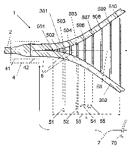
FIG. 1 shows a schematic partial view of a 1-2 or Y-splitter 1 according to
the
invention, wherein a number of transversal elements 501, 502, 503, 504, 505,
506, 507, 508, 509, 510 of varying width and position are inserted between
the two output waveguide arms 301, 302. The splitter comprises an input
core 2, and two output cores 301, 302 connected by a branching part 4
having core refractive index and consisting of a tapered section 41 which
adiabatically adapts the width of the input core to that of the sum of the two
sideways abutted output core widths and an abutting section 42 in which the
output cores abut each other over a certain length before they diverge in path
into the splitting region 7. Alternatively, the two output waveguides may
overlap in the (possibly tapered) branching part (cf. 4 in FIG. 5.b).
Alternatively, the two output waveguides may overlap in the abutting section
42 and may also be tapered. The transversal elements, having core
refractive index, are located in the splitting region 7, i.e. the area between
the
two output waveguides from the Y-splitter, where the waveguides diverge
from each other (as in FIG. 1 ). Alternatively the locations of transversal
elements may extend into the area between the output waveguides where
they run in parallel (the parallel region, cf. 8 in FIGs. 5.a and 5.b). The
signature 70 indicates that the splitting region 7 is continued over a larger
distance than shown in FIG. 1.
The input waveguide core 2, the output waveguide cores 301, 302, the
branching part 4 and the transversal elements 501-510 all have identical core
refractive index and are embedded in a cladding 6, all formed on a substrate
(cf. 10 in FIG. 7).
In the processing of the device, the transversal elements are defined
simultaneously with the waveguide structure. The j'th element has a width 52
of w~ and the separation 54 to the following element is s~. The length 53 in
the
output direction 50 over which the elements are placed is denoted by L.
CA 02488263 2004-12-O1
WO 03/102648 PCT/DK03/00367
The effect of these transversal elements is to give rise to an
"average/effective refractive index". Where in the beginning the elements are
wide and closely spaced, the "average/effective refractive index" is close to
5 the core refractive index. Seen towards the right - in the output direction
50 -
the widths of the elements are reduced (cf. e.g. the widths 51 (w;) of the
i'th
element and 52 (w~) of the j'th element) and the separation of the elements is
increased (cf. e.g. the separation 54 (s~) between the j'th and the (j+1 )'th
element and 55 (Sj+1) between the Q+1)'th and the (j+2)'th element). This in
10 turn gives rise to a lower "average/effective refractive index" that
converges
towards the cladding refractive index. After the length L (as counted from the
location of the first element), the transversal element structure is
terminated,
L being the sum of the individual separation distances s;.
15 FIG. 2 shows the dependence of the wavelength ~, of the total loss
reduction
90 and the loss reduction 91 (cf. notation on the figure) for four different
splitter designs in a 1-16 splitter tree (cf. FIG. 6), each having been
optimized
individually according to the invention compared to corresponding designs
without the transversal element structure.
In order to find the optimum distribution of the transversal elements, their
widths and the length L it is necessary to use iterative calculations. This
iteration is done by in turn varying the individual parameters, and then
calculate the insertion. loss for the component. This has been done for a 1-16
splitter design, and is depicted in FIG. 2. As appears from FIG. 2, the total
loss reduction 90 varies almost linearly with wavelength in the range between
0.5 dB (~,=1.60 Vim) and 0.9 dB (7~=1.26 Vim). The loss reduction per splitter
91 correspondingly vary between approximately 0.1 and 0.2 dB in the same
wavelength range between 1.26 and 1.60 Vim.
FIG. 3 shows measured insertion loss for vertically 95 and horizontally 96
polarized light as well as the polarization dependent loss 97 for a 1-16
splitter
tree according to the invention.
Each of the four splitter designs constituting a 1-16 splitter tree have been
optimized individually over the wavelength range typically of interest. The
CA 02488263 2004-12-O1
WO 03/102648 PCT/DK03/00367
36
loss reduction for the four new designs have been calculated, compared to
the old designs without the transversal element structure in the splitting
region, as well as the total loss reduction. In FIG. 3 measured insertion
losses for light polarized 0° and 90° with respect to vertical,
as well as the
polarization dependent loss (PDL = abs(Losso - Loss9o°)) are shown. As
appears from FIG. 3, PDL 97 varies between 0.05 and 0.23 dB for the 16
outputs. The insertion losses for light polarized 0° 95 vary between -
12.1 and
-12.5 dB, whereas the insertion losses for light polarized 90° 96 vary
between -12.23 and -12.46 dB for the 16 outputs.
FIG. 4 shows an example of an actual layout of a Y splitter 1 according to the
invention. The input 1 is connected to the branching part 4 - comprising a
tapered part 41 and an abutting part 42, the latter consisting of the two
abutted ends of the output waveguide cores 301, 302. A number (more than
30) of transversal elements 5 are inserted between the output waveguide
cores over a length of the splitting region starting from the right after the
abutting part. In determining the location of the first transversal element
following the abutting part in the output direction, the flow properties of
the
materials in question must be considered including the possibility to fill the
relatively small area (volume) between the abutting part and the first
transversal element with cladding material.
FIGs. 5.a and 5.b show examples of 2-4 branching units according to the
invention. The device consists of a X%:(100-X)% field coupler followed by
two 1-2 splitters according to the invention. It is preferred that X is
independent of wavelength and preferably 50. This can be obtained by
proper design of the directional coupler, see, e.g. J.D.Love et. al. Electron.
Lett. 30 (1994) 1853-1854 or A. Takagi et. al. Electron. Lett. 26 (1990) 132-
133.
FIGs. 5.a and 5.b show a 2-4 branching unit 101 comprising a field coupler
210 having two inputs 211, 212 and two outputs that serve as inputs to two
identical 1-2 splitters with inputs 21, 22 joined by a branching part 4 to
outputs 301, 302 and 303, 304, respectively with transversal waveguide core
elements 5 connecting the respective output waveguide cores over a fraction
of the length of the splitting region 7. The output waveguides run in parallel
in
CA 02488263 2004-12-O1
WO 03/102648 PCT/DK03/00367
37
the output direction 50 (defined by the direction of light guidance of the
input
waveguide) over a certain length in the parallel region 8.
In the branching unit of FIG. 5.a, the 2 outputs 301, 302 of an 1-2 splitter
are
sideways abutted in an abutting part 42 of the branching part 4 joining the
input 21 and output 301, 302 waveguide cores. A tapered part 41
adiabatically adapts the combined width of the two output waveguide cores to
the width of the input waveguide core.
FIG. 5.b show a corresponding 2-4 branching unit 101 having the same
structure as the branching unit in FIG. 5.a apart from the branching part 4 of
the 1-2 splitters, which in FIG. 5.b consists of a simple Y-structure
resembling
the points of a train railway, i.e. having one input gradually splitting into
2
outputs, the inputs and outputs having identical 'track-widths').
FIG. 6 shows an example of a 1-16 splitter according to the invention. The
branching unit is composed of 1-2 Y-splitters in a splitter tree. Each 1-2
splitter is provided with a number of transversal waveguide core elements
connecting the 2 output waveguide cores. The loss reduction for individual
parts of the 1-16 splitter is shown in FIG. 2.
The splitter tree of the 1-16 branching unit 110 of FIG. 6 comprises an input
201 and 16 outputs 301-316 (the reference numbers of the 14 outputs
between 301 and 316 are not indicated). The inputs and outputs are joined
by a splitter tree comprising 1-2 splitters at 4 levels as represented by 1-2
splitters 111, 112, 113, 114, each 1-2 splitter comprising transversal output
waveguide core elements inserted for optimum insertion loss. The layout of
each individual splitter may be optimized with respect to a minimum return
loss. Alternatively (or additionally), the insertion loss of the whole layout
may
be minimized in an iterative process by variation of the design parameters for
the component, including the number, location, path, width and separation of
the transversal waveguide core elements of each 1-2 splitter.
FIG. 7 shows a schematic cross sectionalview a branching element
of
according to the inventionformed on substratewith 8 output
a core
waveguides embedded in cladding. 7 showsa cross section
a FIG. of a
CA 02488263 2004-12-O1
WO 03/102648 PCT/DK03/00367
38
planar waveguide structure according to the invention. The cross section is
taken perpendicular to the intended direction of light guidance of the
waveguides. The waveguide structure comprises a substrate 10, e.g. a
silicon wafer, defining a reference plane 11. The substrate carries a number
of waveguides for guiding light comprising a cladding layer 6 in which
waveguide core elements 301-308 are embedded. The waveguide core
elements have a rectangular cross section (within processing tolerances), the
width being taken in a direction parallel to the reference plane 11 as
indicated
by 3081 for waveguide core 308. The thickness of the waveguide core is
given by its dimension in a direction perpendicular to the reference plane 11
as indicated by 3082 for waveguide core 308. The thickness is controlled by
the thickness of the core layer during processing. The 8 waveguide core
cross sections of FIG. 7 may illustrate the 4x2 outputs of 4 1-2 splitters in
a 1-
8 branching unit, i.e. (301, 302) and (303, 304) and (305, 306) and (307, 308)
constituting output waveguide pairs as seen in a cross section of the parallel
region. The opposing edges of two neighbouring output cores may be
represented by edges 3051 and 3061 of output waveguide core pair (305,
306).
FIG. 8 shows a schematic cross sectional view of an optical component
according to the invention. The component is essentially identical to that of
FIG. 7. In FIG. 8, however, the cladding layer 6 is detailed to show a lower
cladding layer 61 formed on a substrate 10 with 8 output waveguide core
sections 301-308 applied to the lower cladding layer 61, the waveguide core
sections and the parts of the lower cladding layer not being covered by the
waveguide core pattern is covered by an upper cladding layer 62.
Additionally the upper cladding layer 62 is shown to have a corrugated
surface 621 due to repeated deposition and annealing steps leading to reflow
of the upper cladding layer (the amplitude is exaggerated in the drawing).
The upper cladding layer has a lower flow temperature than that of the core
and lower cladding layers, controlled by proper addition of boron, phosphorus
and/or fluorine (or any other dopants that reduces the flow temperature) to
the upper cladding layer. The control of the cladding reflow properties is
e.g.
described in R.A. Levy, K. Nassau, "Reflow Mechanisms of Contact Vias in
VLSI Processing", J. Electrochem. Soc., Vol. 133, No. 7, p. 1417 (1986),
which is incorporated herein by reference.
CA 02488263 2004-12-O1
WO 03/102648 PCT/DK03/00367
39
FIG. 9 shows a one to two splitter 1 comprising an input waveguide core
section 2 and output waveguide core sections 301, 302 separated by a
branching part comprising a tapered branching element 41. The branching
element 41 adapts the width of the input core to that of the sum of the two
sideways abutted output core sections. Between the output core sections a
number of transversal elements 501, 502, 503 are positioned. Some of the
transversal elements 502, 503 are segmented, i.e. comprise individual pieces
of core material 555 separated by a space filled with upper cladding material.
The transversal elements are parallel, have decreasing width, increasing
mutual distance and comprise an increasing number of segments with
increasing distance from the splitting point (i.e. the point at the branching
part
where the two output waveguides separate away from each other). Stress
relieving structural elements in the form of pads 340, 341 enclose the outer
edges of the waveguide core sections of the component. The distance 370
between the neighbouring edges of, respectively, the waveguide core
sections (including the branching part) and the stress relieving pads is
around 10 pm.
FIG. 10 shows a schematic partial view of a one to three splitter 1 according
to the invention. The splitter 1 comprises an input waveguide core section 2
and output waveguide core sections 301, 302, 303 separated by a branching
part 41, 42 comprising a tapered branching element 41 and an abutting
section 42. The branching element 41 gradually adapts the width of the input
core to that of the sum of the three sideways abutted output core sections. A
number of transversal elements 501, 502, 503 are positioned. between the
three output core sections 301, 302, 303, the width of the transversal
elements decreasing and their mutual distance increasing in the direction of
light propagation from input to output as indicated by the arrow.50.
Example 1: Fabrication of splitter according to the invention.
In the following a description of one method to fabricate a branching device
according to the invention will be presented.
CA 02488263 2004-12-O1
WO 03/102648 PCT/DK03/00367
First, the core geometry and refractive index difference between core and
cladding materials should be fixed. For applications in telecommunications it
is advantageous that there is as little as possible insertion loss between the
input-/output fibres and the component as well as back-reflections from the
5 fibre-component interface. Low insertion loss and low back-reflection is
achieved by matching the integrated waveguide structure to the fibres in
geometry as well as in refractive indices of the core and cladding materials.
In telecommunication systems typically the Corning SMF-28 or equivalent
fibres are used. Using a commercial numerical mode solver, such as the
10 commercially available Selene from C2V, Enschede, The Netherlands, a
suitable combination of core dimensions and refractive indexes is found. For
good polarization dependence the core cross-sectional shape is typically
quadratic. Now, given the core cross-sectional shape and refractive index
difference the minimum bending radius (radius of curvature) of the splitter
15 output arms can be estimated using e.g. semi-analytical expressions or
better numerical BPM (Beam Propagation Method) methods. The minimum
radius of curvature should be large enough that only a negligible amount of
light is radiated out of the waveguide bend, but not too large as this yields
a
large and space consuming component.
It is advantageous, but in no way necessary, to have a tapering region in
front of the two parting waveguides as this can reduce transition-/radiation
loss from the initial straight waveguide to the bending waveguides.
When the various parts that constitute the traditional splitter have been
chosen to yield a low-loss splitter, the transversal waveguide elements in the
splitting have to be determined.
One method to determine the placement of the transversal elements is to first
choose the length of the transition region L. L should be large enough that
the loss is minimized but not larger than necessary since the remaining
transversal waveguide elements will slightly scatter light from the cores and
do not contribute to confining the light to the core. As a rule of thumb L
should be chosen such that the inner edge-to-edge distance between the
bending waveguides is approximately 2 - 4 times the waveguide core width.
CA 02488263 2004-12-O1
WO 03/102648 PCT/DK03/00367
41
When L is determined the transversal waveguide elements can be placed in
a multitude of ways, however, the width (in the horizontal direction) should
preferably decrease. This could be done e.g. by choosing a maximum (start)
width, a minimum (end) width and a number M of elements, and then let the
width w; and the mutual distance s; be a function of i, where i = 1,2, ..., M.
After the elements have been placed in the design, the total loss is
calculated
using a numerical method e.g. using BPM, e.g. the commercially available
Prometheus from C2V, Enschede, The Netherlands. The widths, spacings
and the number N are subsequently varied iteratively and the loss is
calculated. When a minimum is found the iterations are ended.
Example 2: A variable optical attenuator according to the invention.
A VOA is an important device in network management for levelling multiple
wavelength signals. It can be realised by combining two 1-2 splitters in a
Mach-Zehnder geometry. The phase difference between light that
propagates in the two arms can, e.g., be controlled by the thermo-optic effect
by means of a heater element on one of the arms. Thereby the output
intensity can be controlled. The advantage of the present invention is that
the
un-attenuated signal has low loss. Moreover, because of the better uniformity
of the splitting ratio, a larger dynamic attenuation range can be expected
(more than 25 dB attenuation).
Stress relieving structures:
The stress field across a coupler region is shown in. FIG. 11, represented by
the birefringence in the centre of the core region. ~Ny, ~NX represents the
change of refractive index N in, respectively, the width (y) and height (x)
directions, of a waveguide core section between the anneal temperature and
room temperature. As can be seen there is a noticeable asymmetry of the
birefringence in the waveguide cores (the position of the cores in a cross
section perpendicular to the intended direction of light propagation of the
waveguides are indicated by the black~rectangles 801, 802). This asymmetry
is believed to be one of the causes for un-predicted polarization issues with
CA 02488263 2004-12-O1
WO 03/102648 PCT/DK03/00367
42
directional couplers. To make this birefringence more uniform, stress
relieving structures are added on the outside of the coupler waveguides.
FIG. 12 shows the effect of adding one and two structures (821, 822 and 820,
823, respectively) of 1 pm width at each side of the 6 Nm wide and 6 pm high
coupler waveguides 801, 802, the coupler waveguides being spaced 6 Nm
apart (edge-to-edge). The edge-to-edge distance between a waveguide and
its nearest stress relieving structure is 5 pm and between two stress
relieving
structures likewise 5 Nm. The refractive indices of the waveguide core and
cladding should be suitable for sustaining an optical mode, e.g. substantially
constant (step index profile), preferably more = 1,4520 and n~lad = 1,4450 at
~.
= 1550 nm.
FIG. 13 is a close-up of the birefringence in the coupler waveguides. It is
clearly seen, that adding the stress relieving structures makes the
birefringence more uniform. This is an indication of a more uniform strain
field
across the waveguides.
The width of the stress relieving grooves between a waveguide core section
and a stress relieving structure must be chosen such that no or little light
is
coupled from the waveguides and into the relieving structures. The stress
relieving structures can also be designed as large pads that are positioned
with an appropriate distance to the couplers, e.g. around 10 Nm.
An embodiment of a waveguide coupler according to the invention is shown
in FIG. 14. Here the wide lines 801, 802 are the waveguide core structures
and the narrow lines 810, 811, 812, 813, 820, 821 822, 823 are the stress
relieving structures. The stress relieving structures are positioned around
the
waveguides in the whole coupling region 830 (the central part where the
waveguides are closest). This will give a more uniform strain field. The
stress
relieving structures will additionally have the advantage that the so-called
gap-filling will be easier. This means that void formation in the process of
depositing and reflowing the top-cladding will be eliminated.
Another embodiment of a waveguide coupler 800 according to the invention
is shown in FIG. 15. Here the stress relieving structures are designed as
CA 02488263 2004-12-O1
WO 03/102648 PCT/DK03/00367
43
large pads 840, 841, 842, 843. The pads essentially fill out the (otherwise)
open space between the waveguide core pattern of the coupler. The distance
from a pad 840 to a core 801 is in this case approximately 10 pm.
FIG. 16 shows the birefringence for a coupler as depicted in FIG. 15 with and
without the stress relieving pads (cf. 840, 841, 842, 843 of FIG. 15). Also
here, it is clear that the birefringence asymmetry in the cores is reduced by
the inclusion of the pads.
FIG. 17 shows a coupler 800 according to the invention comprising stress
relieving pads 840, 841 and segmented transversal elements 850 extending
between the waveguide core sections 801, 802 over the coupling length.
Each of the transversal elements 850 comprise a number of individual core
segments 855 separated by a space filled with upper cladding material. The
distance from a pad 840 to a core 801 is in this case approximately 15 pm.
FIG. 18 shows a coupler 800 according to the invention comprising stress
relieving pads 840, 841 and - transversal elements 850 connecting the
waveguide core sections 801, 802 of the coupler over the coupling length
and in the regions of the coupler where the waveguides diverge/merge.
FIG. 19 shows a one to two splitter 1 according to the invention comprising
stress relieving pads 340, 341, 342 surrounding the input 2 and output 301,
302 waveguide sections and the intermediate branching element 41. The
component further comprises transversal elements 5 located between the
output waveguide sections in the splitting region. The distance 370 between
the waveguide core sections (branching element and transversal elements)
and the stress relieving pads is preferably in the range between 5 and 20 pm.
An optical component comprising segmented waveguides and/or waveguides
with transversal elements aimed at gap-filling:
FIG. 21 shows a sketch of a traditional directional coupler 800 with two
separate waveguides 801, 802 closely spaced over a length L~R (the
coupling length) 830. .
CA 02488263 2004-12-O1
WO 03/102648 PCT/DK03/00367
44
FIG. 22 schematically shows two waveguide core sections forming a
directional coupler in a cross section perpendicular to the direction of light
guidance of the waveguides. FIG. 22.a shows a situation where the two
waveguide cores 801, 802 are perfectly covered by an upper cladding layer
62, and FIG. 22.b shows a situation where the two waveguide cores are too
closely spaced and the structure cannot be perfectly filled resulting in void
formation 805 in the upper cladding layer 62 between the two cores 801, 802.
FIG. 23 shows a coupler 800 according to the invention, termed type A. In
the space between the two waveguide cores 801, 802, N angled cross-bars
850 having a width W and a distance between neighbours S, are inserted.
The N cross-bars (where N can be any number from 1 and up, depending on
the actual structure) are inserted symmetrically around the central part of
the
coupling region 805 (the coupling region having the length of LcR). To reduce
back-reflections each of the cross-bars 850 are angled as shown in the insert
figure. The angle a between an angled edge of a cross-bar and a direction
perpendicular to the direction of light propagation may preferably be in the
neighbourhood of 8 degrees. However, the component will function with -45
< a < 45 degrees, which will not impact the effects of improved reflow and
reduced birefringence.
The width W, the number N and the distance between neighbours S depend
on the given geometry of the coupler. It is self-evident that the insertion of
these cross-bars affects the optical coupling between the two waveguide
cores, and the length of the coupling region LcR is calculated numerically
using suitable numerical simulation software. It can be beneficial for optical
loss reduction to distribute the cross-bars in such a way, that they e.g.
primarily are placed in regions in the coupler structure where the optical
intensity is predominantly in one of the waveguide cores and omit cross-bars
in regions where the intensity is predominantly between the two cores. In this
way the cross-bars are less likely to give rise to loss and back-reflections.
The geometry of the embodiment depicted in FIG. 23 is as follows:
~ Edge-to-edge distance between waveguide core sections 801, 802 over
the coupling length LcR 805 is 4 pm.
~ Coupling length LcR 805 is 1000 pm.
~ Core width is 6 Nm. Core height is 6 pm.
CA 02488263 2004-12-O1
WO 03/102648 PCT/DK03/00367
~ The number of cross-bars (also termed transversal elements in other
parts of the present application) is 20.
~ The width of the cross-bars is 2 pm.
~ The angle a is 8°.
5 ~ The centre-to-centre distance between cross-bars is 50 pm.
FIG. 24 shows a coupler 800 according to the invention, termed type B. In a
segment coupler of type B each of the two closely spaced waveguide cores
801, 802 are segmented having N segments 840. Each segment 840 of the
10 embodiment in FIG. 24 have 4 edges 841, 842, 843, 844 constituting a
parallelogram. The segments have the length S and a clearance between
segments of W. The facets in the segments are angled, to reduce back-
reflections, such that the facets form the angle a with vertical (in other
words
two non-opposing sides 842, 843 together define an angle 90+a). Also for
15 this coupler structure the length S and mutual separations W may be
optimized depending upon the actual structure. The distribution of W's and
S's along the coupling region must also in this case be calculated
numerically.
For this type of coupler the considerations regarding the coupler termed Type
20 A applies with minor modifications.
Since there are N punctures (i.e. the spacing between adjacent segments of
core material) where the cladding material can flow more or less freely the
reflow is eased hence a reduced stress-induced birefringence is likely to
25 result (of course depending on the geometries, dimensions, materials and
processing details).
FIG. 25 shows a coupler 800 according to the invention, termed type C. This
coupler type is a combination of the two formerly described types A and B.
In segment coupler of type C the two closely spaced waveguide cores 801,
802 are punctured with N spaces between N-1 segments 840 (as type B).
The N-1 separate waveguide core segments are connected by cross-bars
850 as described for the coupler of type A. Each cross-bar 850 is angled, i.e.
comprises two pieces (or legs) 851, 852 that together define the angle 90+a.
The considerations regarding types A and B apply to type C as well. However,
CA 02488263 2004-12-O1
WO 03/102648 PCT/DK03/00367
46
it is to be expected that this structure is more stable since the segments 840
are connected to each other by cross-bars 850. For this structure all the
appearing variables need be calculated numerically in a recursive loop until
the optimum structure is achieved (e.g. the width of the punctures and of the
cross-bars need not be identical).
FIG. 26 shows a three to three directional coupler 800 comprising transversal
elements 850 between neighbouring waveguide core sections 801, 802, 803
over the coupling length and in the regions of the coupler where the
waveguides diverge/merge.
In general N, W and S are determined from the simple coupler structure as
well as the viscosity of the cladding material during reflow. Using simulation
software as e.g. Prometheus/OlymplOs from C2V the modified coupling
length is easily calculated compared to the traditional/simple structure, and
it
is then possible to design a component which can be realised without voids,
and which exhibit improved (reduced) birefringence.
Fabrication technology
A branching component according to the present invention can be fabricated
in a number of different planar technologies such as in polymers, in Silicon-
on-insulator (SOI), Lithiumniobate (LiNb03), III-V, as well as in silica-on-
Silicon and others. In an embodiment of the present invention the silica-on-
silicon planar technology is used as this technology produces the most
advanced and technically developed planar waveguide components. Silica
waveguides possess a number of highly attractive properties such as
material compatibility (optical fibres are made from the same material,
silica),
optimum coupling between fibre and waveguide component (refractive
indices and index differences are comparable), low absorption- and
propagation losses, low birefringence, high stability and low cost.
Furthermore, the technology used to fabricate these silica waveguides is
identical to the technology used in fabricating integrated electrical circuits
such as CPU's (Central Processing Units in computers) and e.g. RAM
CA 02488263 2004-12-O1
WO 03/102648 PCT/DK03/00367
47
(Random Access Memory), thus this technology has matured during the last
more than thirty years and is known to be capable of mass production.
FIG. 20 shows a flow chart for a method of manufacturing an optical
component according to the invention. The method comprises the steps a) to
f) as discussed in the following.
In an embodiment of the present invention a clean and bare Silicon wafer
(used as substrate, step a) is firstly oxidized (step b) to provide an optical
isolation layer of silica sufficiently thick that the magnitude of the
evanescent
field tail of the field pertaining to the waveguide cores is sufficiently low
to
ensure negligible propagation loss. This first layer of silica is referred to
as
the buffer layer. On top of the buffer layer a layer of doped-silica is
deposited
(step c), containing one or more dopants that effectively act to increase the
refractive index of said layer. This doped layer of silica glass is referred
to as
the core layer. Depending upon the method used to deposit the core layer a
high temperature treatment (known as an anneal step) may be advantageous
in order to stabilize the optical and/or mechanical properties of said layer.
The optical waveguide circuitry is defined through standard optical
lithography where a UV-transparent plate containing typically a chromium
pattern replica of the waveguide design pattern and possible other structural
elements (such as stress relieving and transversal elements) (step d) is
pressed against a layer of UV-sensitive polymer which has been spin coated
onto the surface of the core silica layer, subsequently the UV-sensitive
polymer is exposed through the mask and the pattern is developed (step e).
Following the exposure and development of the waveguide pattern into the
polymer layer, the polymer pattern is used as masking material for dry
etching (e.g. RIE - Reactive Ion Etching, ICP - Inductively Coupled Plasma)
into the core silica layer (step e). Alternatively a second masking material
is
sandwiched between the silica core layer and the UV-sensitive polymer layer,
which is used to enhance selectivity and waveguide core profile. In this way
the design waveguide pattern is transferred into the core silica layer having
predetermined cross-sectional properties as well as refractive index. In order
to protect the recently defined waveguide core, and in order to enhance
symmetry in the structure transverse to the direction of propagation a layer
of
silica with optical properties as close to those of the buffer layer as the
CA 02488263 2004-12-O1
WO 03/102648 PCT/DK03/00367
48
chosen fabrication technology permits is deposited on top of the core
structure (step f). The formation of the latter layer (e.g. termed the upper
cladding layer) may be formed using successive deposition and annealing
steps (step f).
Various relevant aspects of the silica-on-silicon technology is e.g. discussed
in M. Kawachi, "Silica waveguide on silicon an their application to integrated-
optic components", Opt. Quant. Electr. 22 (1990) 391-416, which is
incorporated herein by reference. Various relevant aspects of low loss plama
enhanced chemical vapour deposited planar waveguides are e.g. discussed
in Christian Laurent-Lund, "PECVD grown Multiple Core Planare Waveguides
with Extremely Low Interface Reflections and Losses", Photon. Technol. Lett.
10 (1998) 1431-1433, which is incorporated herein by reference. Various
aspects of the technique of cladding deposition and reflow annealing using
boron-phosphorus silica glass (BPSG) are disclosed in US-6,044,192, which
is incorporated herein by reference.
Some preferred embodiments have been shown in the foregoing, but it
should be stressed that the invention is not limited to these, but may be
embodied in other ways within the subject-matter defined in the following
claims. The components described above are intended for use with light
propagated from input to output. It is, however, possible to reverse the
direction of light propagation, so that light is propagated from an output to
an
input of a component.