Note: Descriptions are shown in the official language in which they were submitted.
CA 02488903 2004-11-29
DC/DC CONVERTER INCLUDING A ZENER DIODE HAVING
A SUBSTANTIALLY ZERO TEMPERATURE COEFFICIENT
This application claims priority to prior Japanese patent application JP
2004-16575, the disclosure of which is incorporated herein by reference.
Background of the Invention:
This invention relates to a DC/DC converter and, in particular, to a step-
down DC/DC converter.
In the manner which is well known in the art, the DC/DC converter is a
power converter for converting a DC voltage (an input DC voltage) having a
voltage level into another DC voltage (an output DC voltage) having anther
voltage level. The DC/DC converter is also called a switching regulator, a
switching power source, or a ringing choke converter. The DC/DC converter
where the output DC voltage has the voltage level higher than that of the
input
DC voltage is called a step-up DC/DC converter. The DC/DC converter where
the output DC voltage has the voltage level lower than that of the input DC
voltage is called a step-down DC/DC converter. This invention relates to the
step-down DC/DC converter.
The step-down DC/DC converter uses a transistor as a switch, switches
the transistor, converts an input DC voltage into an AC voltage, steps the AC
voltage down by using a transformer, and rectifiers it to convert an output DC
voltage.
In general, the DC/DC converter of the type described comprises a
transformer having a primary winding, a secondary winding, and an auxiliary
winding. The auxiliary winding is called a feedback winding, a positive
CA 02488903 2004-11-29
2
feedback winding, a feedback coil, or a base winding. A switching transistor
is
connected in series to the primary winding of the transformer. By making the
switching transistor self-oscillation, energy is transmitted to the secondary
winding. The DC/DC converter further comprises a control transistor for
turning the switching transistor on or off. A feedback control circuit
including a
Zener diode is connected between the control transistor and the auxiliary
winding.
Various DC/DC converters of the type are already known. By way of
example, a switching power source for controlling current characteristics on a
primary side is described in Japanese Published Patent Application (A) No.
H11-98838 or JP 11-98838 A. The switching power source disclosed in JP
11-98838 A realizes stable performance which is independent of an input
voltage and external factors such as environmental temperature. The
switching power source uses, as the above-mentioned Zener diode, a diode
having a positive temperature coefficient (e.g. a "positive temperature
characteristic" where its Zener voltage becomes high when the temperature
becomes high). In addition, the switching power source comprises a
temperature detecting resistor for correcting variations of the current
characteristics due to variations of the environmental temperature. That is,
in
JP 11-98838 A, the switching power source needs the temperature detecting
resistor because of use of the diode having the positive temperature
coefficient
as the Zener diode.
On the other hand, a ringing choke converter is disclosed in Japanese
Published Patent Application (A) No. H8-275523 or JP 8-275523 A. The
ringing choke converter disclosed in JP 8-275523 A comprises, as the Zener
diode, a diode having a negative temperature coefficient (e.g. a "negative
temperature characteristic" where its Zener voltage becomes low when the
temperature becomes high). In JP 8-275523 A, the ringing choke converter
CA 02488903 2004-11-29
3
needs any temperature compensation because of use of the diode having the
negative temperature coefficient as the Zener diode.
In addition, a DC/DC converter is disclosed in Japanese Examined
Utility Model Application Publication (Y) No. S56-5507 or JP 56-5507 Y The
DCIDC converter disclosed in JP 56-5507 Y comprises a Zener diode for
controlling an output voltage without the above-mentioned control transistor.
The above-mentioned JP 56-5507 Y merely discloses the DC/DC converter
which carries out an output voltage control on the primary side of the
transformer but which does not carry out an output current control on the
primary side of the transformer.
Summary of the Invention:
It is therefore an object of the present invention to provide a DC/DC
converter which dose not need a particular part for temperature compensation.
Other objects of this invention will become clear as the description
proceeds.
On describing the gist of an aspect of this invention, it is possible to be
understood that a DC/DC converter comprises a transformer having a primary
winding, a secondary winding, and an auxiliary winding, a switching transistor
connected in series to the primary winding of the transformer, a control
transistor for turning the switching transistor on or off, and a feedback
control
circuit connected between the control transistor and the auxiliary winding of
the
transformer. The feedback control circuit includes a Zener diode.
According to the aspect of this invention, in the above-mentioned
DC/DC converter, the Zener diode has a substantially zero temperature
coefficient. Preferably, the Zener diode may have a Zener voltage which lies
in
a range between 5 volts and 6 volts. Desirably, the temperature coefficient of
said Zener diode may be selected so as to cancel a temperature characteristic
of the control transistor.
CA 02488903 2004-11-29
4
In addition, each of the switching transistor and the control transistor
may be composed of, for example, an npn-type bipolar transistor. In this
event,
the switching transistor has a collector connected to an end of the primary
winding while the switching transistor has an emitter which is grounded. The
control transistor has a collector connected to a base of the switching
transistor,
while the control transistor has an emitter which is grounded. The auxiliary
winding has an end which is grounded. The feedback control circuit is inserted
between another end of the auxiliary winding and a base of the control
transistor. The feedback control circuit may comprise, for example, the Zener
diode which has an anode connected to a base of the control transistor and a
cathode connected to the other end of the auxiliary winding, and a resistor
connected in parallel to the Zener diode.
Alternatively, the feedback control circuit may comprise the Zener diode
having an anode connected to a base of the control transistor, a first
resistor
having an end connected to a cathode of the Zener diode, a second resistor
which has an end connected to the base of the control transistor and another
end connected to another end of the first transistor, and a third resistor
connected between the other end of the second resistor and the other end of
the auxiliary winding. The above-mentioned DC/DC converter further may
comprise a capacitor having an end which is grounded, and a second Zener
diode which has an anode connected to another end of the capacitor and a
cathode connected to the base of the switching transistor.
Brief DescriQti~n of th~Drawing_
Fig. 1 is a circuit diagram of a DC/DC converter according to a first
embodiment of this invention;
Fig. 2 is a view showing a temperature characteristic of the DC/DC
converter illustrated in Fig. 1; and
CA 02488903 2004-11-29
Fig. 3 is a circuit diagram of a DC/DC converter according a second
embodiment of this invention.
Description of the Preferred Embodiments:
In the manner which is described above, the conventional DC/DC
converters use, as a Zener diode, a diode having a positive or a negative
temperature coefficient. Therefore, it is understood that various temperature
compensations are necessary to the conventional DC/DC converters.
Accordingly, the present co-inventors reached an idea that uses, as the
Zener diode, a diode having a substantially zero temperature coefficient.
Now, attention will be directed to a Zener diode. There are two causes
why current flows abruptly when a voltage is applied to the Zener diode in a
reverse direction. One cause is a Zener breakdown due to a tunnel effect.
Another cause is an avalanche breakdown due to an avalanche effect. The
Zener diode is a diode where both effects are mixed little by little. The
Zener
breakdown dominates in the Zener diode having a relatively low Zener voltage
while the avalanche breakdown dominates in the Zener diode having a
relatively high Zener voltage. Both of the Zener breakdown and the avalanche
breakdown are mixed at a proper rate in the Zener diode having the Zener
voltage of about 5 volts.
The description will proceed to a temperature characteristic of the Zener
diode. The tunnel effect has a negative temperature coefficient. The
avalanche effect has a positive temperature coefficient. As a result, the
temperature characteristic of the Zener diode largely changes dependent on the
Zener voltage. Inasmuch as the tunnel effect and the avalanche effect are
effective at the similar rate when the Zener voltage is equal to about 5
volts, the
both temperature coefficients are cancelled to each other, whereby the Zener
voltage hardly changes even if the temperature changes.
CA 02488903 2004-11-29
6
On the other hand, the above-mentioned control transistor has a
temperature characteristic. In general, a transistor has a negative
temperature
characteristic of -2mVl°C which is generally used. As a result, it is
necessary
to take account of the temperature characteristic of the control transistor
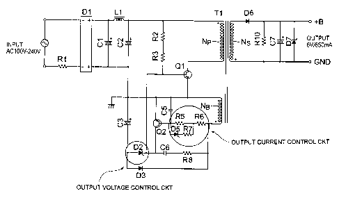
Referring to Fig. 1, the description will proceed to a DCIDC converter
according to a first embodiment of shit invention. The illustrated DC/DC
converter comprises a transformer T1 having a primary winding NP, a
secondary winding Ns, and an auxiliary winding NB.
The DCIDC converter includes, on a primary side of the transformer T1,
a rectifying circuit D1, a first input capacitor C1, an input inductor L1, a
second
input capacitor C2, a switching transistor Q1, a control transistor Q2, a
control
feedback circuit (which will later be described), and so on. The first input
capacitor C1, the input inductor L1, and the second input capacitor C2
constitute a smoothing circuit.
An AC power source is connected to the rectifying circuit D1 through a
resistor R1. The illustrated AC power source generates, as an input AC
voltage, a voltage between 100 volts and 240 volts. The input AC voltage is
rectified by the rectifying circuit D1, is smoothed by the above-mentioned
smoothing circuit, and is stored in the second input capacitor C2 as an input
DC
voltage.
The switching transistor Q1 is connected in series to the primary
winding NP of the transformer T1. Specifically, the second input capacitor C2
has an end connected to an end of the primary winding NP of the transformer
T1.
The illustrated switching transistor Q1 consists of an npn-type bipolar
transistor.
The primary winding NP of the transformer T1 has another end connected to a
collector of the switching transistor Q1. The switching transistor Q1 has an
emitter which is grounded. Resistors R2 and R3 are connected in series
between a base of the switching transistor Q1 and the end of the second input
CA 02488903 2004-11-29
7
capacitor C2.
The input DC voltage is applied to the primary winding NP of the
transformer T1 to turn the input DC voltage on or off by the switching
transistor
Q1. The control transistor Q2 is for turning the switching transistor Q1 on or
off.
Between the control transistor Q2 and the auxiliary winding NB of the
transformer T1, the feedback control circuit, which will be presently
described, is
connected.
The control transistor Q2 consists of an npn-type bipolar transistor.
The feedback control circuit comprises resistors R5, R6, R7 and a Zener diode
D5. The resistors R5 and R6 are connected in series between a base of the
control transistor Q2 and one end of the auxiliary winding NB of the
transformer
T1. The resistor R7 and the Zener diode D5 are connected in series between
both ends of the resistor R5.
The control transistor Q2 has an emitter which is grounded. Between
the base and the emitter of the control transistor Q2, a capacitor C5 is
connected. Between the end of the auxiliary winding NB of the transformer T1
and an collector of the control transistor Q2, a resistor R8 and a capacitor
C6
are connected in series. The collector of the control transistor Q2 is
connected
to the base of the switching transistor Q1.
A capacitor C3 has an end which is grounded. The capacitor C3 has
another end which is connected to the base of the switching transistor Q1
through a Zener diode D2 and which is connected to the end of the auxiliary
winding NB of the transformer T1 through a diode D3. In other words, between
both ends of the diode D3, the Zener diode D2, the capacitor C6, and the
resistor R8 are connected in series.
As one part in the feedback control circuit, the Zener diode D5 has a
diode having a substantially zero temperature coefficient. More specifically,
the Zener diode D5 has a Zener voltage which lies in a range between 5 volts
CA 02488903 2004-11-29
8
and 6 volts. As a result, the illustrated DC/DC converter does not need a
particular part for temperature compensation.
In addition, the feedback control circuit serves as an output current
control circuit while the Zener diode D2 serves as an output voltage control
circuit.
The DC/DC converter comprises, on a secondary side of the
transformer T1, a diode D6, a resistor R10, an output capacitor C7, and a
Zener
diode D7. The secondary winding NS of the transformer T1 has an end
connected to a grounding terminal GND of the DC/DC converter and another
end connected to a power source terminal +B of the DC/DC converter through
the diode D6. The resistor R10, the capacitor C7, and the Zener diode D7 are
connected in parallel between the power source terminal +B and the grounding
terminal GND.
Induced in the secondary winding NS of the transformer T1, an AC
voltage is rectified by the diode D6 and is smoothed by the output capacitor
C7
to produce a secondary output voltage between the power source terminal +B
and the grounding terminal GND.
In the example being illustrated, the DC/DC converter produces the
secondary output voltage of 6 volts and can flow an output current of 650
milliamperes from the power source terminal +B.
According to the DC/DC converter having the above-mentioned
structure, it is possible to control the output constant voltage and the
constant
current on the primary side of the transformer T1 in the manner which will
later
be described and to stabilize the output concerning input fluctuations of the
AC
input voltage (100 volts to 240 volts).
First, the description will be made as regards a constant voltage control.
A minus voltage of the auxiliary winding NB of the transformer T1 is
controlled
by the Zener diode D2 to control the secondary output voltage at a constant.
CA 02488903 2004-11-29
9
By making coupling between the secondary winding NS and the auxiliary
winding NB of the transformer T1 good, the input fluctuations of the AC input
voltage is improved.
Subsequently, the description will be made as regards a constant
current control. By adjusting a base current of the control transistor Q2 by
the
feedback control circuit (the output current control circuit), a collector
current of
control transistor Q2 is controlled so as to control the output current. By
adding the Zener diode D5 having the substantially zero temperature
coefficient,
the input fluctuations of the AC input voltage is improved.
!n the manner which is described above, the control transistor Q2 has
the temperature characteristic. Accordingly, the temperature coefficient of
the
Zener diode D5 is selected so as to cancel the temperature characteristic of
the
control transistor Q2. As a result, as a whole of the DC/DC converter, a
stable
current characteristic is realized.
Fig. 2 shows a temperature characteristic of the output voltage in the
DC/DC converter illustrated in Fig. 1. In Fig. 2, the abscissa represents
temperature [°Cj and the ordinate represents current [mA]. Fig. 2 shows
results measured at three temperatures of -20°C, 25°C, and
60°C. It may be
understood that results change linearly at intermediate temperatures.
A temperature characteristic illustrated in Fig. 2 is obtained as follows.
The DC/DC converter (product) used to measure has a rated output
voltage/output current of 5.3 volts/600 milliamperes. When the output current
flows 600 milliamperers or more, the output voltage reduces gradually. Date
shown in Fig. 2 represent current values measured on a time when the output
voltage is equal to 3.6 volts. That is, by changing the environmental
temperature of the produce and by measuring the current value when the output
voltage becomes 3.6 volts, the temperature characteristic shown in Fig. 2 is
obtained.
CA 02488903 2004-11-29
In the manner which is apparent from Fig. 2, the measured results are
settled in a dispersion range within about 10% at a temperature range between
-20°C and 60°C. From such a fact, it is understood that the
temperature
characteristic is adjusted in a range where can sufficiently use as actual
products.
Although both controls of the output current control and the output
voltage control are carried out on the primary side of the transformer in the
DC/DC converter according to the first embodiment of this invention
illustrated
in Fig. 1, only the output current control may be carried out on the primary
side
of the transformer in a DCIDC converter according to a second embodiment of
this invention which will later be described.
Referring to Fig. 3, the description will proceed to the DC/DC converter
according to the second embodiment of this invention. The same reference
symbols are attached to those having similar functions to those illustrated in
Fig.
1.
The AC power source is connected to the rectifying circuit D1 through a
fuse F2. The illustrated AC power source generates an input AC voltage of AC
100 volts. The output terminals of the rectifying circuit D1 are connected to
a
smoothing circuit which consists of the first input capacitor C1, a first
inductor
L1, the second input capacitor C2, and a second inductor L2.
The smoothing circuit has an end connected to an end of the primary
winding NP of the transformer T1. The primary winding NP of the transformer
T1 has another end connected to the collector of the switching transistor Q1.
The switching transistor Q1 has a base connected to the end of the primary
winding NP of the transformer T1 through the resistors R3 and R2 which are
connected in series to each other. Between the base and the emitter of the
switching transistor Q1, a diode D10 is connected. The emitter of the
switching transistor Q1 is grounded through a fuse F1.
CA 02488903 2004-11-29
11
The emitter of the switching transistor Q1 is connected to an end of the
auxiliary winding NB of the transformer T1. Another end of the auxiliary
winding NB of the transformer T1 is connected to the base of the control
transistor Q2 through a feedback control circuit (an output current control
circuit).
The feedback control circuit comprises a parallel circuit which consists of
the
resistor R5 and a series circuit consisting of the Zener diode D5 and the
resistor
R7. Both ends of the auxiliary winding NB of the transformer T1, a capacitor
C9 and a diode D11 are connected in series. Between a connecting point of
the capacitor G9 and the diode D11 and the base of the control transistor Q2,
a
Zener diode D9 and a resistor R15 are connected in series. Between the other
end of the auxiliary winding Ns of the transformer T1 and the collector of the
control transistor Q2, the resistor R8 and the capacitor C6 are connected in
series. The collector of the control transistor Q2 is connected to the base of
the switching transistor Q1. The emitter of the control transistor Q2 is
connected to the base of the switching transistor Q1 through the diode D10.
On the other hand, the secondary winding NS of the transformer T1 has
an end connected to the power source terminal +B through a parallel circuit
consisting of the diode D6 and a capacitor C9 and an inductor L2. The
secondary winding Ns of the transformer T1 has another end which is
connected to the grounding terminal GND. Between the power source terminal
+B and the grounding terminal GND, the capacitor C7 and the Zener diode D7
are connected in parallel. In addition, between the power source terminal +B
and the grounding terminal GND, a capacitor C18 is connected.
The DC/DC converter produces the secondary output voltage between
the power source terminal +B and the grounding terminal GND. In the
example being illustrated, the DC/DC converter produces the secondary output
voltage of 5.6 volts and can flows an output current of 700 milliamperes from
the power source terminal +B.
CA 02488903 2004-11-29
12
The DCIDC converter according to the second embodiment of this
invention comprises a photocoupler IC1 for feeding the output voltage on the
secondary side back to the primary side. The photocoupler IC1 comprises a
photodiode and a phototransistor. The description will be made as regards a
circuit for feeding back the output voltage.
Between the power source terminal +B and the grounding terminal GND,
a resistor R17 and a Zener diode D8 are connected in series. A connecting
point between the resistor R17 and the Zener diode D8 is connected to a
cathode of the photodiode of the photocoupler IC1. The photodiode of the
photocoupler IC1 has an anode which is connected to the grounding terminal
GND through a capacitor C8 and which is connected to the power source
terminal +B through a resistor R12 and the inductor L2.
On the other hand, the phototransistor of the photocoupler IC1 has a
collector which is connected to the other end of the auxiliary winding NB of
the
transformer T1 through the diode D11 and which is connected to the base of the
control transistor Q2 through a series circuit consisting of the diode D9 and
the
resistor R15. The phototransistor of the photocoupler IC1 has an emitter
connected to the base of the control transistor Q2 through a resistor R12.
At any rate, the DC/DC converter according to the second embodiment
of this invention carries out the output voltage control by feeding the output
voltage on the secondary side of the transformer T1 back to the primary side
of
the transformer T1 by using the photocoupler IC1.
In the DC/DC converter according to the second embodiment of this
invention, the Zener diode D5 as one part in the feedback control circuit has
a
diode having a substantially zero temperature coefficient. More specifically,
the Zener diode D5 has a Zener voltage which lies in a range between 5 volts
and 6 volts. As a result, the illustrated DC/DC converter does not need a
particular part for temperature compensation.
CA 02488903 2004-11-29
13
In addition, in the manner which is described above, the control
transistor Q2 has the temperature characteristic. Accordingly, the temperature
coefficient of the Zener diode D5 is selected so as to cancel the temperature
characteristic of the control transistor Q2. As a result, as a whole of the
DC/DC converter, a stable current characteristic is realized.
Now, the description will be made as regards an output current control
in the DC/DC converter having such a structure. It will be assumed that the
output current of the DC/DC converter increases. In proportion to the output
current, a voltage is induced in the auxiliary winding NB of the transformer
T1.
By the induced voltage, a current flowing through the resistor R5 in the
feedback control circuit turns the control transistor Q2 on or off. By
controlling
the switching transistor Q1 by turning the control transistor Q2 on/off, the
output
current control is carried out.
While this invention has thus far been described in conjunction with a
few preferred embodiments thereof, it will now readily possible for those
skilled
in the art to put this invention into various manners. For example, the
feedback control circuit may be not restricted to those in the above-mentioned
embodiments.