Note: Descriptions are shown in the official language in which they were submitted.
CA 02491913 2005-O1-06
WO 2004/012484 PCT/US2003/023697
PRINTED CIRCUIT BOARD ASSEMBLY HAVING A BGA CONNECTION
Field of the Invention
This invention relates to a printed circuit board assembly having a ball grid
array (BGA) connection.
Background of the Invention
Ball grid array connectors are generally known in the art and a general
discussion of such connectors can be found in United States Patent No.
5,730,606, which
is hereby incorporated by reference. These types of connectors generally
include fusible
elements, preferably spherical solder balls, that are positioned on electrical
contact pads of
a circuit substrate or disposed within a ball pocket. The plurality of solder
balls is
generally referred to as a ball grid array. An integrated circuit may be
mounted to a plastic
or ceramic substrate PCB Materials (FR-4) and electrically connected to the
ball grid
array. Among the advantages of ball grid array connectors are smaller package
sizes, good
electrical performance and lower profiles.
Ball grid arrays have been used in connection with printed circuit boards.
For example, FCI Electronics, Inc.'s United States patent nos. 6,183,301 B1
and 6,083,047
disclose printed circuit boards having a ball grid array connection and are
hereby
incorporated by reference. Broadly, this invention relates-to an improved
electrical
connector having an improved BGA connection. In an embodiment, this invention
relates
to improved printed circuit board assemblies that have an improved connection
between
the traces of the printed circuit board and the fusible elements or solder
balls.
Summary of the Invention
An electrical connector of this invention includes a housing, which has a
base, at least one circuit board, at least one fusible element, and a metallic
element. The at
least one circuit board is disposed witlun the housing and includes at least
one signal trace.
The at least one fusible element is disposed within the housing base, and the
metallic
element couples a first end of the signal trace to the at least one fusible
element. Although
the metallic elements may have a number of embodiments, the metallic element
preferably
has a pair of arms between which at least one circuit board fits.
CA 02491913 2005-O1-06
WO 2004/012484 PCT/US2003/023697
2
The connector may also have at least one solder pad that couples the
metallic element to the signal trace first end. Preferably, the solder pad is
disposed on part
of one lateral face of the circuit board. In another preferred embodiment, the
connector
has another solder pad disposed on the other lateral face of the solder pad,
so that the
metallic element is in contact with both solder pads to place the printed
circuit board signal
trace in electrical communication with the at least one fusible element.
In a preferred embodiment, at least one circuit board includes a module that
can be inserted into and removed from the housing. Preferably, the at least
one circuit
board is inserted into a slot in the housing base, and the metallic elements
are disposed
within the base slot.
Preferably, the housing base has holes disposed within each slot that
correspond to each signal trace of the printed circuit bond assembly. Disposed
beneath
each hole is a pocket in which a fusible element is disposed. Each of the
metallic elements
preferably extend from a slot, through a hole, and into a pocket. Thus, an
electrical
comlection is made from the signal trace, to the metallic element, and to the
fusible
element. Another electrical component can be mated with the connector by
mating
contacts of pads of the other electrical component with the fusible elements.
In other preferred embodiments, the metallic elements are not used. In
these embodiments, the circuit board assembly is inserted into a base slot and
solder paste
is heated and flows within the base slot to form an electrical connection
between the solder
paste and the circuit board signal traces. The solder paste also flows through
the base and
into contact with the fusible element. Thus, an electrical connection is
formed from the
PCB signal traces to the solder paste and to the fusible elements.
Other features of the invention are set forth below.
Brief Description of the Drawings
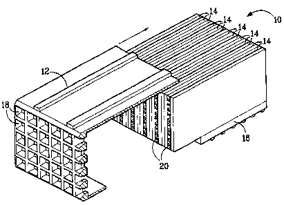
Figure 1 is an assembly view of a connector according to a preferred
embodiment of this invention;
Figure 2 is an assembly view of a portion of the preferred embodiment of
Figure 1;
Figure 3 is an perspective top view of a preferred embodiment of the base
portion of the connector of Figure 1;
Figure 3A is an enlarged view of detail 3A of Figure 3;
Figure 4 is a perspective bottom view of the base of Figure 3;
Figure 5 is an assembly view of a printed circuit board and a base according
to a preferred embodiment of this invention;
Figure SA is an assembly view of a printed circuit board and a base
according to a second preferred embodiment of this invention;
CA 02491913 2005-O1-06
WO 2004/012484 PCT/US2003/023697
Figure SB is a cross-section taken through one of the base pockets of Figure
5A with the assembly installed;
Figure 6A is an assembly view of a printed circuit board and a base
according to a second preferred embodiment of this invention;
Figure 6B is a cross-section taken through one of the base pockets of Figure
6A with the assembly installed; and
Figure 7 is a side view of the preferred embodiment of the connector of
Figure 1 being connected to an electrical component.
Detailed Description of Preferred Embodiments
Figurel depicts an assembly of a preferred embodiment of an electrical
connector 10 according to a preferred embodiment of this invention. Although
it need not
be, the connector 10 is in the embodiment shown a right angle connector. The
connector
10 preferably has a housing 12, a plurality of printed circuit board
assemblies 14, and a
base 16. Preferably, the printed circuit board assemblies 14 are removeable
from the
housing 12.
In the preferred embodiment of Figure 1, the connector 10 has five printed
circuit board assemblies 14. The connector 10 of this invention can have any
number of
printed circuit boards 14, and eleven are shown for illustrative purposes. The
printed
circuit boards 14 can have a number of applications and circuits depending
upon their
application.
Figure 1 depicts a portion of an embodiment of the housing 12. The
housing 12 can be made from any suitable material such as a thermoplastic. The
housing
12 has a plurality of lead in holes 18. The lead in holes are for receiving a
terminal of a
mating connector (not shown). The housing 12 may have any number of lead in
holes, and
therefore only a portion of the housing 12 is shown in Figure 1. As shown,
each of the
lead in holes 18 is aligned with a contact terminal 20 of a printed circuit
board assembly
14.
The printed circuit board assemblies 14, which are best shown in Figure 2,
each preferably include a substrate 16 that has a plurality of signal traces
22 and a plurality
of ground traces 24. The substrate 16 may have a ground contact that is in
communication
with the ground trace 24. The ground contact is preferably a fusible element,
and even
more preferably a solder ball. In a preferred embodiment, a plurality of
printed circuit
board pads 28 may be attached to the signal traces 22. In other preferred
embodiments,
solder pads are not used. Preferably, the printed circuit board pads 28 are
constructed
from solder. Disposed over the substrate may be a dielectric material which
may be an
insulating spacer 30. Disposed over the insulating spacer may be an insulating
cover 32.
CA 02491913 2005-O1-06
WO 2004/012484 PCT/US2003/023697
4
The dielectric material 30 and the insulating cover 32 are attached to the
substrate 16 to
form a printed circuit board assembly 14 as shown in Figure 2. Disposed at an
end of each
signal trace 22 is a contact terminal 20. As shown in Figures 1 and 2, the
contact terminals
20 are aligned with the housing lead in holes 18. The contact terminals 20 are
for
receiving a corresponding contact of another connector to make an electrical
connection
between the signal traces 22 and another electrical component.
Shown in the perspective views of Figures 3 and 4 is the housing base 16,
which is attached to the printed circuit board assemblies 14 as shown in
Figure 1. Figure 3
is a perspective view of the top of the base 16, and Figure 4 is a perspective
view of the
bottom of the base 16. The housing base 16 is preferably constructed of a high
temperature plastic material. Although the base 16 need not be, the base 16 is
preferably
constructed as a single piece and is molded. The base 16 serves to form a
connection
between the signal traces 22 and the ground trace 24 and another electrical
element, such
as a printed circuit board, as shown (and explained below) in the cross-
sectional view of
Figure 6.
As shown in Figure 3, there may be a plurality of slots 36 disposed within
the base 12. Each of these slots 36 receives a printed circuit board assembly
14 as shown
in the assembly drawing of Figure SA. Although only one printed circuit board
assembly
14 is shown as being inserted into one slot 36 in Figure 5, it will be
appreciated that a
printed circuit boaxd assembly 14 is disposed in each base slot 36 as shown in
Figure 1. It
will further be appreciated that the base 16 could have any number of slots
36.
Disposed within each of the slots 36 are a plurality of holes 38. There is a
hole 38 for each signal trace 22 of a printed circuit board, as is best
understood from
Figure 5. Any number of holes can be used. The holes 38 extend from the top of
the base
to the pockets 39 disposed in the bottom of the base, as understood with
reference to
Figures 3, 4 and SA. As opposed to the base top, the bottom of the base is
preferably flat
and does not have slots.
Figure SB is a cross-section taken through one of the pockets 39 of Figure
SA with the assembly installed and is representative of each pocket. As shown
one of the
metallic elements 44 extends down through a hole 38 into the pocket 39. In the
preferred
embodiment shown, the hole 38 is smaller in diameter or in cross section than
the pocket
39. This is because the hole 38 needs only to be large enough to receive the
prong 44,
while the pocket 39 needs to be large enough to house the fusible element 48.
The shape
and the size of the holes 38 and pockets 39 can be varied, however, to fit any
suitable
metallic element 44 and fusible element 48.
In a preferred embodiment, there is a metallic element 40 disposed in each
hole 38. The metallic elements 40 extend from the top of the base through a
hole 38 and
CA 02491913 2005-O1-06
WO 2004/012484 PCT/US2003/023697
into the base pockets 39 as shown in Figures 3 and 4. The metallic elements 40
may take
any of a variety of shapes. For example, as shown in Figure 5, the metallic
elements 42
may have a single prong 44 which extends through to the bottom of the hole,
and a pair of
prongs 46 that are electrically connected to a signal trace of the circuit
board, as shown in
5 Figures 5 and 6. Preferably, each of the printed circuit board assemblies 14
has a solder
pad 28 disposed over the lower portion of the lateral face. The solder pads 28
are in
electrical connection with the signal traces 22. The pair of prongs 46 can
contact the
solder pads, thereby placing the signal traces 22 in electrical connection
with the metallic
elements 40.
Disposed within each pocket 39 is a fusible element 48, as shown in Figure
4. When the connector 10 is attached to another element such as another
circuit board, the
fusible elements 48 provide an electrical connection between the signal traces
22 of the
printed circuit board assemblies and the circuits of the second element. The
fusible
elements 48 are preferably solder balls. Each of the fusible elements 48 are
disposed
within one of the base pockets 39. The metallic elements' single prongs 44
extend into the
pockets so that when the fusible element is melted it attaches to the
respective single prong
44 in the base pocket 39 to form an electrical connection.
Illustrated in Figure 7 is a schematic cross sectional view depicting the
mating of the connector 10 to another electrical component 50, which in the
embodiment
shown is a printed circuit board. Figure 7 also depicts the electrical
connections between
the electrical component 50, the fusible elements 48, and the circuit board
assemblies 14.
As shown, each of the fusible elements 48 of the printed circuit board
assembly 14 extends
proximal to a corresponding receptacle 52, which is preferably a solder pad,
of the mating
printed circuit board assembly 50. Thus, an electrical connection is provided
between the
printed circuit board 10 and the mating printed circuit board assembly 50. The
mating
printed circuit board assembly 50 is provided here by way of example. It will
be
appreciated that numerous other mating assemblies or connectors can be used
with the
assembly 10 and the assembly SO is used here for illustrative purposes.
As shown, the assembly 14 is inserted into a base slot 36, and fits between
the prongs 46 of the metallic element 40. The solder pads 28 contact one of
the prongs 46
to make an electrical connection between the assembly signal traces and the
metallic
element 40. The single prong 44 extends from the pair of prongs 46 and the
slot 36 into
the pocket 39, where it is attached to a fusible element 48. As shown, the
hole 38 may be
narrower than the pocket 39 and houses the single prong 44, while the pocket
39 houses
the larger fusible element 48. Disposed within the slot 36, the hole 38 and
the pocket 39
may be solder paste which is melted to fuse the metallic element 40, solder
pads 28, and
fusible elements to each other.
CA 02491913 2005-O1-06
WO 2004/012484 PCT/US2003/023697
6
Connector 50 as described above mates with the base 16. Figure 7 also
shows the contact 52 of connector mated with the fusible element 48.
In another preferred embodiment, which is shown in Figures 6A and 6B,
metallic elements 44 are not used. These figures are similar to Figures SA and
SB except
that no metallic element 40 is used. Each printed circuit board assembly 14 is
inserted into
a base slot 36. Solder paste 70 or another suitable material is disposed
within the slot 36
and in the base holes 38 and pockets 39. The solder paste 70 is heated so that
it flows in
the slot 36, the holes 38 and the pockets 39, and adheres to the solder pads
or the signal
traces. The solder paste 70 then provides an electrical connection from the
signal traces to
the fusible elements. Solder pads need not be used, but may be used in this
embodiment.
The method of forming the connector 10 preferably includes assembling
each of the printed circuit board assemblies 14, and then inserting each
printed circuit
board assembly 14 into a housing 12. This includes disposing each of the
signal traces
between the prongs of a metallic element 40, if a metallic element 40 is used.
This is
accomplished by inserting the circuit board assemblies into the base slots.
Solder paste if
used is heated and flows in the slots 36 and around the signal traces and
metallic elements
40. Each of the fusible elements 48 is then inserted into the housing base
pockets 39. The
base 16 is attached to the printed circuit board assemblies, and the base 16
and assemblies
14 are attached to the housing 12. An electrical component is then aligned
with the base
16 and attached to the base 16. This includes forming the electrical
connection between
each fusible element 48 and a corresponding element of the electrical
connector 50 by
heating and flowing the fusible elements 48 to form the electrical
connections, as shown in
Figure 5.
An advantage of one embodiment of this invention that uses metallic
components 40 to make the electrical connection between the circuit board
assemblies 14
and the solder balls 48 is that the metallic components 40 provide better more
reliable
connections than solder balls 48 melted and adhered directly to the circuit
board
assemblies 14. Moreover, the metallic elements 40 provide better lateral
support for the
circuit board assemblies 14.
An advantage of embodiments of this invention that employ the base 16 is
that the base 16 provides a mating structure between the circuit board
assemblies 14 and
another electrical component 50. The base houses the solder balls, provides a
structure on
which to mount the circuit board assemblies, and provides discrete pockets for
melting the
solder balls to obtain a reliable connection between the solder balls and the
electrical
component 50.
The broad sense of this invention includes a printed circuit board assembly
10 that has fusible elements on a wall of the printed circuit board. It is to
be understood,
CA 02491913 2005-O1-06
WO 2004/012484 PCT/US2003/023697
7
however, that even though numerous characteristics and advantages of the
present
invention have been set forth in the foregoing description, together with
details of the
structure and function of the invention, the disclosure is illustrative only,
and changes may
be made in detail, especially in matters of shape, size and arrangement of
parts within the
principles of the invention to the full extent indicated by the broad general
meaning of the
terms in which the appended claims are expressed.