Language selection

Search

Patent 2491919 Summary

Third-party information liability

Some of the information on this Web page has been provided by external sources. The Government of Canada is not responsible for the accuracy, reliability or currency of the information supplied by external sources. Users wishing to rely upon this information should consult directly with the source of the information. Content provided by external sources is not subject to official languages, privacy and accessibility requirements.

Claims and Abstract availability

Any discrepancies in the text and image of the Claims and Abstract are due to differing posting times. Text of the Claims and Abstract are posted:

  • At the time the application is open to public inspection;
  • At the time of issue of the patent (grant).
(12) Patent Application: (11) CA 2491919
(54) English Title: A METHOD OF REALIZING COMMUNICATING BETWEEN MODULES OF SYSTEM DEVICES
(54) French Title: PROCEDE DE COMMUNICATION ENTRE MODULES DE DISPOSITIFS DE SYSTEME
Status: Dead
Bibliographic Data
(51) International Patent Classification (IPC):
  • H04L 12/44 (2006.01)
  • H04L 49/351 (2022.01)
  • H04Q 1/20 (2006.01)
  • H04L 49/201 (2022.01)
  • H04L 12/24 (2006.01)
  • H04L 12/56 (2006.01)
  • H04L 29/14 (2006.01)
(72) Inventors :
  • SHI, XINMING (China)
(73) Owners :
  • HUAWEI TECHNOLOGIES CO., LTD. (China)
(71) Applicants :
  • HUAWEI TECHNOLOGIES CO., LTD. (China)
(74) Agent: GOWLING WLG (CANADA) LLP
(74) Associate agent:
(45) Issued:
(86) PCT Filing Date: 2003-04-24
(87) Open to Public Inspection: 2004-01-15
Examination requested: 2005-01-05
Availability of licence: N/A
(25) Language of filing: English

Patent Cooperation Treaty (PCT): Yes
(86) PCT Filing Number: PCT/CN2003/000300
(87) International Publication Number: WO2004/006591
(85) National Entry: 2005-01-05

(30) Application Priority Data:
Application No. Country/Territory Date
02123683.6 China 2002-07-08

Abstracts

English Abstract


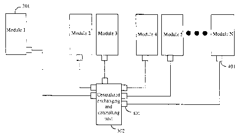
The invention disclosed a method of realizing communicating between modules of
system devices, particularly relates to : setting a centralized exchanging and
controlling unit in the devices , connecting the each modules in the devices
to the centralized exchanging and controlling unit through respective
communicating and controlling interface ; when communicating among the
modules, resource module send the signal to centralized exchanging and
controlling unit , after processing by the centralized exchanging and
controlling unit send the signal to destination module. In the invention,
because each module directly connected to the centralized exchanging and
controlling unit in singles, and adopting the communicating and controlling
interface of high-speed to communicate, then the method have so many advantage
,for example, the ability to communicate among any modules, the high
reliability, easy to locate where is accident, no limit to the number of
modules, easily to design and so on.


French Abstract

L'invention concerne un procédé de communication entre modules de dispositifs de système, visant en particulier à mettre en place une unité centralisée d'échange et de contrôle dans les dispositifs, et à relier les modules des dispositifs à cette unité via des interfaces respectives de communication et de contrôle. Dans la communication entre ces modules, un module source transmet le signal à l'unité considérée qui, après traitement, transmet à son tour le signal au module de destination. Le procédé offre de nombreux avantages, car chaque module est relié directement à ladite unité, utilisant par ailleurs une interface de communication et de contrôle grande vitesse, ce qui assure une communication intermodule fiable et permet de déceler aisément les défaillances, sans limitation du nombre de modules, sur la base d'une conception simple, entre autres.

Claims

Note: Claims are shown in the official language in which they were submitted.


Claims

1. A Method of realizing communicating between modules of system devices,
wherein:
setting a centralized exchanging and controlling unit in device;
connecting the centralized exchanging and controlling unit with every module
through communication control interface of the module in the device;
when communicating between the modules, sending the message to the
centralized exchanging and controlling unit by a source module, processing the
message by the centralized exchanging and controlling unit, and forwarding the
processed message to a destination module by the centralized exchanging and
controlling unit.
2. The method according to the Claim 1, further comprising:
broadcasting the message by the centralized exchanging and controlling unit,
comparing the destination address of the message with address of the module by
each
module in device, and if the two addresses are identical, receiving the
message by the
module.
3. The method according to the Claim 2, further comprising:
presetting address pins of each module, and getting address of the module by
reading the current state of address pins by each module.
4. The method according to the Claim 3, further comprising:
presetting the state of address pins in each module by setting the voltage
state on
the backplane circuit.
5. The method according to the Claim 1, wherein:
sending the message from a source module to a destination module directly
through exchanging by the centralized exchanging and controlling unit .

7

Description

Note: Descriptions are shown in the official language in which they were submitted.


CA 02491919 2005-O1-05
PCT/CN03/00300
A Method of Realizing Communicating between Modules of
System Devices
Field of the Technolo~y
The invention relates to the internal communication within devices, especially
a
method of realizing communicating between modules of system devices.
Background of the Invention
In larger devices, such as transmission facilities, exchange devices and
wireless
base stations etc., the modules have direct or indirect connection, so it is
necessary to
communicate between the modules frequently. The communication information
includes not only those for normal service, but also those for maintenance,
such as
alarm, fault detection etc.
At present, there are two ways for communication between modules in devices:
The first way is to communicate through a mailbox, as shown in figure 1. The
control module 101 is connected with every module 102 through the data bus,
address
bus and control bus, and because the mailbox can bi-directional communicate,
the
control module 101 can make communication with every module 102.
The second way is shown in figure 2. The control module 201 is connected with
every module 202 through the 485 buses, and the communication can be
implemented
through the 485 buses between the module 201 and every module 202, or between
different modules of 202.
Although the bus mode of the above two ways has a simple structure that is
easy
to implement, and supports various protocols, but there are several
disadvantages as
follow: the load capacity of a bus is limited, so it does not support
communication of
many modules; if a fault happens at a point, it is easier that the whole bus
cannot
communicate or the communication reliability become worse, and also it is
difficult to
locate the fault point; furthermore, since there are many connection lines,
the back-
plane circuit design and layout are complex.
Summary of the Invention
1


CA 02491919 2005-O1-05
PCT/CN03/00300
In view of the above-mentioned facts, objective of the invention is to provide
a
method of realizing communicating between modules of system devices in order
that
a large amount of modules can reliably communicate with each other and a fault
is
easy to be located.
To archive the above objective, technical scheme of the invention is as
follow:
A method of realizing communicating between modules of system devices,
wherein:
Setting a centralized exchanging and controlling unit in device;
Connecting the centralized exchanging and controlling unit with every module
through its own communication control interface in the device;
When communicating between the modules, sending the message to the
centralized exchanging and controlling unit by a source module, processing the
message by the centralized exchanging and controlling unit, and forwarding the
processed message to a destination module by the centralized exchanging and
controlling unit.
The method further comprising:
Broadcasting the message by the centralized exchanging and controlling unit,
comparing the destination address of the message with its own address by each
module in device, and if the two addresses are identical, receiving the
message by the
module.
The method further comprising:
Presetting address pins of each module, and getting its own address by reading
the current state of address pins by each module.
The method further comprising:
Presetting the state of address pins in each module by setting the voltage
state on
the backplane circuit.
Wherein:
Sending the message from a source module to a destination module directly
through exchanging by the centralized exchanging and controlling unit.
In the invention, every module is directly connected with the centralized
exchanging and controlling unit with high-speed communication control
interfaces, so
comparing with the present technique, the invention can implement any two
modules
2


CA 02491919 2005-O1-05
PCT/CN03/00300
communication, achieve high reliability, locate a fault point easily, also,
because of
the invention, the number of the modules that take part in the communication
is
unlimited, the system design is simple, easier and flexible.
Brief Description of the Drawings
Figure 1 shows a structure diagram of one way that implements communication
between the modules with the present technique.
Figure 2 shows a structure diagram of another way that implements
communication between the modules with the present technique.
Figure 3 shows the system structure diagram of the invention.
Figure 4 shows an implementation structure diagram of the invention.
Figure 5 shows principle diagram of an embodiment in the invention.
Figure 6 shows principle diagram of another embodiment in the invention.
Embodiments of the Invention
The invention will be described in more detail with reference to drawings and
embodiments.
Figure 3 shows a system structure diagram of the invention. In this diagram,
modules 1 to N are modules 301 that need to communicate with each other within
the
device, and every module is connected with the centralized exchanging and
controlling unit 302, respectively. During communication, a message is
transmitted
from a source module of the modules 301 to the centralized exchanging and
controlling unit 302, the centralized exchanging and controlling unit 302
processes the
message and then forwards the processed message to the destination module in
the
modules 301. Said message includes not only service message, but also
maintenance
message, such as alarm and fault detection messages etc.
3


CA 02491919 2005-O1-05
PCT/CN03/00300
Figure 4 shows an implementation diagram of the invention. In this diagram,
there are the modules 301, the centralized exchanging and controlling unit 302
and the
communication control interfaces 401 that are individually located on each
module
301 and the centralized exchanging and controlling unit 302. Each module 301
takes
its interface 401 to connect with the centralized exchanging and controlling
unit 302,
and communicates each other through the centralized exchanging and controlling
unit
302. Taking the communication between modules 1 and 3 as an example, the
specific
communication procedure is as follows: through the interface 401, the module 1
transmits a message with the module 3 address to the centralized exchanging
and
controlling unit 302; the centralized exchanging and controlling unit 302
receives the
message through the interface 401; after processing, the centralized
exchanging and
controlling unit 302 forwards the message to the destination module 3.
In fact, the invention takes the thought of forming net in a local area
network to
the internal communication of device, and the centralized exchanging and
controlling
unit servers as the central network unit, other modules communicate each other
through the centralized exchanging and controlling unit, therefore, the
centralized
exchanging and controlling unit may take the HUB structure or SWITCH structure
to
perform its functionalities.
When applying a HUB as the centralized exchanging and controlling unit, the
connection between the HUB and the modules is the same as the connection shown
in
figure 4, the only difference is that the HUB substitutes the centralized
exchanging
and controlling unit 302 and the lOM or 100M Ethernet interface substitutes
the
interface 401; figure 5 shows the detail implement procedure. In figure 5, the
Ethernet
interface SO1, which is leaded from every module 301 that need to communicate,
is
connected to the HUB 502 through the backplane circuit; and the HUB 502
comprises:
the transformer 503, the physical layer 504 and the message regenerating and
broadcasting unit 505. Taking communication between the module 1 and the
module
3 as an example which lOM Ethernet interface 501 is applied, the communication
procedure is as follows: the module 1 sends a message with the module 3
address to
the HUB 502 through lOM Ethernet interface 501; in the HUB 502, the message
passes the transformer 503, which makes isolation and impedance
transformation, and
the physical layer 504, which implements the carrier interception, code
conversion
4


CA 02491919 2005-O1-05
PCT/CN03/00300
and collision detect; and then the message enters the regenerating and
broadcasting
unit 505 that makes message amplification, shaping; and then the message is
sent to
every module 301 through the physical layer 504, the transformer 503 and the
Ethernet interface 501. When the message is coming, every module 301 compares
the
destination address in the message and its address; if the two addresses are
different,
the message is rejected; when the message is coming to the module 3, and the
two
addresses are identical as a result of the comparing, the module 3 receives
the
message. The communication between other modules 301 in device is also as
described above. In the above communication procedure, each module 301 needs
to
know its address because the HUB 502 cannot implement the function of
recognizing
address and storing so as to implement the communicatian with the modules 301
in
the manner of broadcasting; in this embodiment, it is implemented by setting
state on
the address pins of a module with backplane circuit to preset each module
address
uniquely, every module gets its address from the current state on the address
pins,
wherein every module has its unique address pins.
In order to transmit easily and support the communication between more
modules, a SWITCH structure severs as the centralized exchanging and
controlling
unit in figure 4. The connection between the SWTTCH and the modules is the
same as
the connection shown in figure 4, the only difference is that the SWITCH
substitutes
the centralized exchanging and controlling unit 302 and the Ethernet interface
501
substitutes the interface 401; figure 6 shows the implement procedure. In
figure 6,
every module 301 is connected with the SWITCH 601 through the Ethernet
interface
501, and the SWITCH 601 is a two layers exchange that includes: the
transformer 602,
the physical layer 603, the exchange part 604 and the Synchronous Dynamic RAM
(SDRAM) 605. The transformer 602 and the physical layer 603 have the same
functions as the transformer 503 and the physical layer 504 in the figure 5.
The
exchange part 604 mainly performs the address self-learning function and the
packet
exchange function, and the SDRAM 605 stores an address table and the packets.
Suppose the embodiment takes a lOM Ethernet interface 501, and when taking
communication between the module 1 and the module 3 as an example, the
communication procedure is as follows: a message with module 3 address is sent
from
the module l; the message passes the lOM Ethernet interface 501, the
transformer 602,
the physical layer 603 and enters the exchange part 604 in which the message
is
5


CA 02491919 2005-O1-05
PCT/CN03/00300
packed and exchanged, and then the packet and the address table are stored in
the
SDRAM 605; after that it is waiting for an idle output line; once there is an
idle line,
the message packet is sent out by the SDRAM 605 along the path: the exchange
part
604, the physical layer 603, the transformer 602 and the Ethernet interface
501. What
difference with the HUB 502 is that the SWITCH 601 can process messages of
multiple modules 301 simultaneously and has self-learning ability: once the
message
is processed by the SWITCH 601, the exchange part 604 will store the address
of the
processed message in the SDRAM 605 automatically. Therefore, when the module
301 is a destination module of a message for the first time, the exchange part
604 of
the SWITCH 601 store the address of the destination module, when processing
later,
according to the address table stored in the SDRAlI~ 60~, the message can be
sent to
the corresponding destination module directly by the SWITCH 601. When a module
is a destination module of a message for the first time, the SWITCH 601
broadcasts
the message to all modules 301 to find out which one matches the destination
module
in the message, and the procedure is same as those in the embodiment of the
figure 5.
The advantages of using SWITCH are that the SWITCH has better utility of
bandwidth and supports multiple modules communication simultaneously, and the
advantages of using HUB are low cost, simple and reliable.
All mentions above are some better embodiments, and they do not limit the
protection scope of the invention.
6

Representative Drawing
A single figure which represents the drawing illustrating the invention.
Administrative Status

For a clearer understanding of the status of the application/patent presented on this page, the site Disclaimer , as well as the definitions for Patent , Administrative Status , Maintenance Fee  and Payment History  should be consulted.

Administrative Status

Title Date
Forecasted Issue Date Unavailable
(86) PCT Filing Date 2003-04-24
(87) PCT Publication Date 2004-01-15
(85) National Entry 2005-01-05
Examination Requested 2005-01-05
Dead Application 2008-12-15

Abandonment History

Abandonment Date Reason Reinstatement Date
2007-12-13 R89 - Failure to Respond
2007-12-13 R30(2) - Failure to Respond
2007-12-13 R29 - Failure to Respond
2008-04-24 FAILURE TO PAY APPLICATION MAINTENANCE FEE

Payment History

Fee Type Anniversary Year Due Date Amount Paid Paid Date
Request for Examination $800.00 2005-01-05
Application Fee $400.00 2005-01-05
Maintenance Fee - Application - New Act 2 2005-04-25 $100.00 2005-01-05
Registration of a document - section 124 $100.00 2005-06-22
Maintenance Fee - Application - New Act 3 2006-04-24 $100.00 2006-04-10
Maintenance Fee - Application - New Act 4 2007-04-24 $100.00 2007-04-10
Owners on Record

Note: Records showing the ownership history in alphabetical order.

Current Owners on Record
HUAWEI TECHNOLOGIES CO., LTD.
Past Owners on Record
SHI, XINMING
Past Owners that do not appear in the "Owners on Record" listing will appear in other documentation within the application.
Documents

To view selected files, please enter reCAPTCHA code :


To view images, click a link in the Document Description column. To download the documents, select one or more checkboxes in the first column and then click the "Download Selected in PDF format (Zip Archive)" or the "Download Selected as Single PDF" button.

List of published and non-published patent-specific documents on the CPD .

If you have any difficulty accessing content, you can call the Client Service Centre at 1-866-997-1936 or send them an e-mail at CIPO Client Service Centre.


Document
Description 
Date
(yyyy-mm-dd) 
Number of pages   Size of Image (KB) 
Abstract 2005-01-05 1 22
Claims 2005-01-05 1 35
Drawings 2005-01-05 3 51
Description 2005-01-05 6 280
Representative Drawing 2005-03-14 1 6
Cover Page 2005-03-15 1 44
Claims 2006-06-02 2 50
Claims 2006-10-16 2 51
PCT 2005-01-05 4 175
Assignment 2005-01-05 3 90
Correspondence 2005-03-11 1 26
Assignment 2005-06-22 4 106
Prosecution-Amendment 2005-12-05 3 79
Fees 2006-04-10 1 40
Prosecution-Amendment 2006-06-02 6 195
Prosecution-Amendment 2006-08-08 2 56
Prosecution-Amendment 2006-10-16 7 222
Fees 2007-04-10 1 40
Prosecution-Amendment 2007-06-13 4 142