Note: Descriptions are shown in the official language in which they were submitted.
CA 02492199 2005-O1-10
WO 2004/008202 PCT/US2003/020202
-1 -
SCHEME FOR CONTROLLING POLARIZATION IN WAVEGUIDES
The present invention relates to the propagation, modulation, and switching
of optical signals in optical devices and, more particularly, to the
polarization of the
optical signals. Modern telecommunications networks, for example, utilize a
variety of optical components to affect propagation, modulation, and switching
of
optical signals and the present invention presents a scheme for enhancing the
performance of such networks by controlling the polarization of the optical
signals
in the network. For the purposes of defining and describing the present
invention,
it is noted that polarization "control" is not limited to mere alteration of
the
polarization state of an optical signal but contemplates, among other things,
polarization-specific attenuation, delay, or other polarization-specific
treatment of
an optical signal as well.
The polarization direction of light propagating in optical fiber and the
associated optical components is usually unknown and may fluctuate over time.
For this reason, optical components that switch, attenuate, amplify or process
the
light in the optical fiber need to carry out their function without regard to
polarization or, in other words, be polarization independent. This leads to
requirements for low polarization dependent loss (PDL) and low polarization
mode
dispersion (PMD). Unfortunately, many optical components have polarization
dependence due to mechanical disturbances, environmental fluctuations, or
asymmetries in the geometrical properties of the component, to name a few.
Many embodiments of the present invention present a means for addressing PDL,
PMD, and other polarization-related perFormance issues in optical components.
In accordance with one embodiment of the present invention, an integrated
optical device is provided. The device comprises: (i) first and second optical
waveguide arms arranged to define an optical signal splitting region near an
input
side of the integrated optical device and an optical signal combining region
near
an output side of the integrated optical device and (ii) a functional region
between
the optical signal splitting and combining regions. The first optical
waveguide arm
CA 02492199 2005-O1-10
WO 2004/008202 PCT/US2003/020202
-2-
comprises a first waveguide core passing through a first electrooptic portion
of the
functional region. The second optical waveguide arm comprises a second
waveguide core passing through a second electrooptic portion of the functional
region. A first set of control electrodes are positioned to generate an
electric field
in the first portion of the functional region. A second set of control
electrodes are
positioned to generate an electric field in the second portion of the
functional
region. The first set of control electrodes, the first waveguide core, and the
first
portion of the functional region are configured such that a TE electromagnetic
polarization mode of an optical signal propagating along the first waveguide
core
encounters an electrooptically induced change in refractive index that is more
predominant than an electrooptically induced change in refractive index
encountered by a TM electromagnetic polarization mode of the optical signal
propagating along the first waveguide core. The second set of control
electrodes,
the second waveguide core, and the second portion of the functional region are
configured such that a TM electromagnetic polarization mode of an optical
signal
propagating along the second waveguide core encounters an electrooptically
induced change in refractive index that is more predominant than an
electrooptically induced change in refractive index encountered by a TE
electromagnetic polarization mode of the optical signal propagating along the
second waveguide core.
In accordance with another embodiment of the present invention, an
integrated optical device configured for splitting TE and TM modes of an
optical
signal is provided. The device comprises: (i) first and second optical
waveguide
arms arranged to define an optical signal splitting region near an input side
of the
integrated optical device and an optical signal combining region near an
output
side of the integrated optical device, (ii) a functional region between the
optical
signal splitting and combining regions, and (iii) a controller coupled to the
functional region. The controller is programmed to establish the voltages
applied
to the first and second sets of control electrodes to affect optical coupling
at the
CA 02492199 2005-O1-10
WO 2004/008202 PCT/US2003/020202
-3-
optical signal combining region of TE and TM polarized portions of the optical
signals propagating along the first and second waveguide cores such that one
of
the first and second waveguide cores following the optical signal combining
region
includes an enhanced TE signal while the other of the first and second
waveguide
cores following the optical signal combining region includes an enhanced TM
signal.
In accordance with yet another embodiment of the present invention, a
method of operating an integrated optical device configured for splitting TE
and
TM modes of an optical signal is provided. According to the method, suitable
voltages are applied to the first and second set of control electrodes
associated
with respective ones of two optical waveguide arms to TE and TM predominant
portions of a functional region of the waveguide device. The voltages applied
to
the first and second sets of control electrodes are established to affect
optical
coupling at the optical signal combining region of TE and TM polarized
portions of
the optical signals propagating along the first and second waveguide cores
such
that one of the first and second waveguide cores following the optical signal
combining region includes an enhanced TE signal while the other of the first
and
second waveguide cores following the optical signal combining region includes
an
enhanced TM signal.
In accordance with yet another embodiment of the present invention, an
integrated optical device configured for variable optical attenuation of an
optical
signal is provided. In this embodiment of the present invention, the optical
device
includes a controller is programmed to establish the voltages applied to the
first
and second sets of control electrodes to affect selective attenuation of TE
and TM
polarized portions of an optical signal coupled to an input port of a selected
one of
the waveguide cores on the input side of the integrated optical device. In
this
manner, the TE and TM polarized portions of the optical signal are attenuated
to
substantially equal extents at an output port of the selected waveguide core
on the
output side of the integrated optical device.
CA 02492199 2005-O1-10
WO 2004/008202 PCT/US2003/020202
-4-
In accordance with yet another embodiment of the present invention, a
method of operating an integrated optical device configured for variable
optical
attenuation of TE and TM modes of an optical signal is provided. According to
the
method, voltages are applied to the first and second sets of control
electrodes to
affect selective attenuation of TE and TM polarized portions of an optical
signal
coupled to an input port of a selected one of the waveguide cores on the input
side of the integrated optical device, such that the TE and TM polarized
portions
of the optical signal are attenuated to substantially equal extents at an
output port
of the selected waveguide core on the output side of the integrated optical
device.
In accordance with yet another embodiment of the present invention, an
integrated optical device configured to control delay in respective TE and TM
modes of polarization of an optical signal is provided. The device comprises a
polarization splitter, a polarization combiner, and a delay section. The
polarization
splitter is configured to direct a TE mode of an input optical signal to a
first optical
waveguide arm of the device and a TM mode of the input optical signal to a
second optical waveguide arm of the device. The polarization combiner is
configured to combine the TE mode of the first optical waveguide arm with the
TM
mode of the second optical waveguide arm into an output optical signal. The
delay section is positioned in a propagation path between the polarization
splitter
and the polarization combiner and is configured to affect a relative phase
delay
between the TE mode of polarization in the first optical waveguide arm and the
TM mode of polarization in the second optical waveguide arm.
In accordance with yet another embodiment of the present invention, a
method of controlling delay in respective TE and TM modes of polarization of
an
optical signal in an integrated optical device is provided. The method
comprises
(i) splitting TE and TM polarized components of an optical signal with a
polarization splitter by directing a TE mode of an input optical signal to a
first
optical waveguide arm of the device and directing a TM mode of the input
optical
signal to a second optical waveguide arm of the device; (ii) combining the
split TE
CA 02492199 2005-O1-10
WO 2004/008202 PCT/US2003/020202
-5-
and TM modes of polarization with a polarization combiner by combining the TE
mode of the first optical waveguide arm with the TM mode of the second optical
waveguide arm into an output optical signal; and (iii) prior to combining the
TE and
TM modes of polarization, affecting a relative phase delay between the TE mode
of polarization in the first optical waveguide arm and the TM mode of
polarization
in the second optical waveguide arm in a delay section in a propagation path
between the polarization splitter and the polarization combiner.
In accordance with yet another embodiment of the present invention, an
integrated optical device configured to convert a selected TE or TM mode of
polarization of an optical signal is provided. The device comprises a
polarization
splitter, a polarization rotator, a delay section, and an output coupler. The
polarization splitter is configured to direct a TE mode of an input optical
signal to a
first optical waveguide arm of the device and a TM mode of the input optical
signal
to a second optical waveguide arm of the device. The polarization rotator is
positioned in one of the first and second optical waveguide arms to rotate a
polarization mode of an optical signal following propagation through the
polarization splitter. The delay section is in a propagation path between the
polarization splitter and the polarization combiner and is configured to
affect a
relative phase delay between signals in the first and second optical waveguide
arms. The output coupler is configured to combine optical signals of the first
and
second optical waveguide arms following propagation through the delay section.
In accordance with yet another embodiment of the present invention, a
method of converting a selected TE or TM mode of polarization of an optical
signal in an integrated optical device is provided. The method comprises the
steps of (i) splitting TE and TM polarized components of an optical signal
with a
polarization splitter by directing a TE mode of an input optical signal to a
first
optical waveguide arm of the device and directing a TM mode of the input
optical
signal to a second optical waveguide arm of the device; (ii) rotating a mode
of
polarization of one of the TE and TM polarized components in one of the first
and
CA 02492199 2005-O1-10
WO 2004/008202 PCT/US2003/020202
-6-
second optical waveguide arms following propagation of the optical signal
through
the polarization splitter; (iii) causing a relative phase delay between
optical signals
in the first and second optical waveguide arms following the rotation of one
of the
TE and TM polarized components of the optical signal; and (iv) combining
optical
signals of the first and second optical waveguide arms following causation of
the
relative phase delay.
In accordance with yet another embodiment of the present invention an
optical network is provided comprising at least one transmitter, at least one
receiver, a network of transmission lines interconnecting the transmitter and
the
receiver, and at least one integrated optical device according to the present
invention.
In accordance with yet another embodiment of the present invention an
optical network is provided comprising at least one transmitter, at least one
receiver, a network of transmission lines interconnecting the transmitter and
the
receiver, at least one optical component, a polarization dependent phase
shifter,
and a phase shift controller. The optical component is configured to introduce
a
polarization dependent phase delay in an optical signal propagating through
the
optical network. The controller is programmed to compensate for the
polarization
dependent phase delay introduced by the optical component by inducing a
suitable change in the refractive indices encountered by the TE and TM
polarization modes of the optical signal.
Accordingly, it is an object of the present invention to provide a variety of
optical waveguide devices that utilize polarization control to enhance the
functionality of the devices and systems employing the devices. Other objects
of
the present invention will be apparent in light of the description of the
invention
embodied herein.
The following detailed description of specific embodiments of the present
invention can be best understood when read in conjunction with the following
CA 02492199 2005-O1-10
WO 2004/008202 PCT/US2003/020202
-7-
drawings, where like structure is indicated with like reference numerals and
in
which:
Figs. 1A and 1B illustrate electrode/core configurations according to the
present invention;
Fig. 2 illustrates relative electrooptic effect as a function of the position
of a
waveguide core within a contoured electric field;
Figs. 3A and 3B illustrate an integrated optical device according to one
embodiment of the present invention;
Figs. 4A-4E illustrate a number of suitable alternative structures for
splitting
and combining optical signals;
Fig. 5A illustrates the operational characteristics of one specific voltage
controlled polarization splitter/switch according to the present invention;
Fig. 5B is a graph illustrating the calculated response of a polarization
splitter/switch as a function of common voltage applied to both sets of
control
electrodes of an optical device according to the present invention;
Fig. 6 illustrates relative positioning of control electrodes and waveguide
cores for an optical device according to the present invention;
Fig. 7 is a schematic illustration of a multiple wavelength optical system
incorporating variable optical attenuators;
Fig. 8 is a graph illustrating polarization dependent loss as a function of
attenuation for a typical thermooptic waveguide variable optical attenuator;
Fig. 9 is a schematic representation of an integrated optical device
configured to control polarization delay;
Fig. 10 is a graph illustrating the calculated relationship between change in
delay for the TE signal, the TM signal and the difference between the two;
Fig. 11 is a graph illustrating examples of delays as a function of voltage
for
several different fixed length difFerences;
Fig. 12 is schematic illustration of an integrated optical device according to
one embodiment of the present invention;
CA 02492199 2005-O1-10
WO 2004/008202 PCT/US2003/020202
_g_
Figs. 13A-13H are schematic illustrations of a variety of electrode/core
configurations according to the present invention; and
Fig. 14 is an illustration of an optical network according to the present
invention.
Functional cladding materials can be utilized in optical waveguide devices
to alter the effective refractive index of the optical waveguide. Although the
present invention is specifically illustrated in the context of an optical
waveguide
including an electrooptic functional cladding material, the functional
material may
be thermooptic, electrooptic, magnetooptic, or another controllable optical
material. For the purposes of defining and describing the present invention,
it is
noted that the wavelength of "light" or an "optical signal" is not limited to
any
particular wavelength or portion of the electromagnetic spectrum. Rather,
"light"
and "optical signals," which terms are used interchangeably throughout the
present specification and are not intended to cover distinct sets of subject
matter,
are defined herein to cover any wavelength of electromagnetic radiation
capable
of propagating in an optical waveguide. For example, light or optical signals
in the
visible and infrared portions of the electromagnetic spectrum are both capable
of
propagating in an optical waveguide. An optical waveguide may comprise any
suitable signal propagating structure. Examples of optical waveguides include,
but are not limited to, optical fibers, slab waveguides, and thin-films used,
for
example, in integrated optical circuits.
In the context of an electrooptically clad waveguide, the refractive index of
the waveguide changes under application of an electric field. The change in
refractive index is dependent on the orientation of the applied electric
field, the
orientation of the electrooptic coefficient of the cladding material, and the
orientation of the light propagating along the waveguide. In some electrooptic
materials, such as electrooptic crystals (i.e. lithium niobate), the
orientation of the
electrooptic coefficient is fixed while the crystal is being grown. However,
in some
electrooptic polymers, the orientations of the electrooptic coefficients are
set
CA 02492199 2005-O1-10
WO 2004/008202 PCT/US2003/020202
_g_
during the poling process or vary as a function of applied electric field and
can be
made to form any number of orientations.
A number of waveguide/electrode configurations are discussed below with
reference to Figs. 1A-1 B and 13A-13H. The positioning of the waveguide within
the contoured electric field alters the relative efficiency of the
electrooptic
interaction with the two dominant polarizations. In some configurations, the
TE
polarization is altered more than the TM polarization. In other orientations,
the
opposite is true. For the purposes of describing and defining the present
invention, it is noted that TE and TM polarized light represent two
independent
electromagnetic modes of an optical signal. The electromagnetic field
distribution
is referred to as the transverse electric (TE) mode where the electric field
of the
optical signal is perpendicular to the plane extending along the primary axis
of
propagation of the waveguide core. The electromagnetic field distribution is
referred to as the transverse magnetic (TM) mode where the magnetic field of
the
optical signal is perpendicular to the plane extending along the primary axis
of
propagation of the waveguide core. It is also noted that in a channel
waveguide of
the illustrated type, the propagating modes are not purely TE or TM polarized.
Rather, the modes are typically more predominantly one or the other and are
commonly so designated. Accordingly, a TE polarized mode may merely
comprise a distribution where the electric field component parallel to the
plane of
propagation is the largest component of the signal. Similarly, a TM polarized
mode may merely comprise a distribution where the magnetic field component
parallel to the plane of propagation is the largest component of the signal.
Electrooptic polymers can be poled in a contour to provide an electrooptic
effect that is dependent on the position of the waveguide core within the
contour.
At positions where the contoured electric fields are predominately horizontal,
the
electrooptic effect will predominately alter TE polarized light. To a lesser
extent
(about 1/3) these horizontal fields will also affect the TM polarized light.
At
positions where the contoured electric fields are predominately vertical, the
CA 02492199 2005-O1-10
WO 2004/008202 PCT/US2003/020202
-10-
electrooptic effect will predominately alter the TM polarized light. Again, to
a
lesser extent (about 1/3), these vertical fields will affect the TE polarized
light.
Figs. 1 A and 1 B show two different waveguide/electrode configurations
where a waveguide device 10 is provided including a functional cladding
material
14 surrounding a core 12 and supported by a silica slab 15 and protected by an
overlayer 19. First and second control electrodes 16, 18 are positioned to
define
an electric field across the functional cladding material 14. The intensity
cross
section of an optical signal propagating along the waveguide device 10 is also
illustrated in Figs. 1A and 1B. The specific compositions forming the
components
of the present invention are beyond the focus of the present invention and may
be
gleaned from state of the art waveguide technology. It is noted however, that
electrooptic materials suitable for use in the present invention as the
functional
cladding material 14 should have an index of refraction that is lower than the
index
of the waveguide core bounded by the cladding layers. Such low-index materials
are described in copending U.S. Patent Publication No. US 2002/0185633
entitled
FUNCTIONAL MATERIALS FOR USE IN OPTICAL SYSTEMS, the disclosure of
which is incorporated herein by reference.
Generally, the polymeric electrooptic materials disclosed in the above-
noted patent application include thermoplastic or thermosetting polymers that
are
blended or co-polymerized with an electrooptic chromophore. The thermoplastic
or thermosetting polymer is typically selected from the group consisting of
acrylics
/ methacrylics, polyesters, polyurethanes, polyimides, polyamides,
polyphosphazenes, epoxy resins, and hybrid (organic-inorganic) or
nanocomposite polyester polymers. Combinations of thermoplastic and
thermosetting polymers (interpenetrating polymer networks) are also
contemplated. The thermoplastic and/or thermosetting polymers typically have
glass transition temperatures above 100°C. One embodiment for low-index
materials has a refractive index value less than 1.5 while another embodiment
for
high-index materials has a refractive index value greater than 1.5. The
polymers
CA 02492199 2005-O1-10
WO 2004/008202 PCT/US2003/020202
-11-
are combined with chromophores, either as part of the backbone chain or
blended
and typically contain compatibilization additives or groups and/or adhesion-
promotion additives or groups. The electrooptic chromophore according to the
invention is typically a substituted aniline, substituted azobenzene,
substituted
stilbene, or substituted imine.
In Fig. 1A, the waveguide device 10 includes a core 12 located between
the first and second control electrodes 16, 18 at a position where the
electric field
E is predominately horizontal. In such a configuration, TE oriented light will
be
altered more than TM oriented light. In the configuration of Fig. 1 B, the
waveguide 10 includes a core 12 located closer to one of the electrodes 16, 18
at
a position where the electric field E is predominately vertical. In such a
configuration, the TM oriented light is altered more than the TE oriented
light.
Figure 2 shows the relative electrooptic effect as a function of the position
of the waveguide core 12 within the contoured electric field E. In this
example, the
electrodes 16, 18 are positioned 15 micrometers apart and the top of the
waveguide core 12 is positioned 3 microns below the plane of the electrodes
16,
18. As is illustrated in Fig. 2, when the waveguide core 12 is positioned
between
the electrodes 16, 18 in the manner illustrated in Fig. 1A, the TE polarized
light is
influenced about 3 times as much as the TM polarized light. Similarly, when
the
waveguide core 12 is positioned directly beneath one of the electrodes 16, 18
in
the manner illustrated in Fig. 1 B, the TM polarized light is influenced about
3 times
as much as the TE polarized light.
Polarization Splitter/Switch.
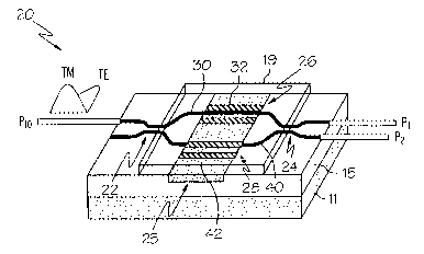
Referring now to Figs. 3A and 3B, an integrated optical device 20
according to one embodiment of the present invention is illustrated. As is
described in detail below, the device of Figs. 3A and 3B is configured to
split TE
and TM polarizations of an optical signal input at Pro and direct the
respective
modes of polarization selectively to a first output port at P~, a second
output port
CA 02492199 2005-O1-10
WO 2004/008202 PCT/US2003/020202
-12-
at P2, or both output ports at P~ and P~. Specifically, Fig. 3 shows an
integrated
optical device 20 having first and second optical waveguide arms 30, 40
arranged
to define a first directional coupling region 22 near an input side of the
integrated
optical device 20 and a second directional coupling region 24 near an output
side
of the integrated optical device 20.
A functional region 25 is defined between the first and second coupling
regions 22, 24 and includes first and second electrooptic portions 26, 28
corresponding respectively to the first and second waveguide arms 30, 40.
First
and second sets of control electrodes are associated with respective ones of
the
first and second electrooptic portions 26, 28 of the functional region 25. The
first
and second electrooptic portions 26, 28 may be rendered electrooptic by the
presence of an electrooptic cladding 14, as is illustrated in Figs. 1A and 1B,
or an
electrooptic waveguide core 16, or both. In any case, it will be appropriate
to
describe and define a waveguide core as "passing through" an electrooptic
portion
of the functional region, regardless of whether the core, cladding, or both
the core
and the cladding, are composed of an electrooptic material. Generally, the
integrated optical device 20 includes a substrate 11, a silica slab 15, the
functional
region 25, and an insulative overlayer 19 and takes the form of a modified
Mach-
Zehnder interferometer configured for electrooptic control in each of the arms
30,
40.
Although many embodiments of the present invention are illustrated herein
with reference to optical signal splitters and combiners in the form of
directional
coupling regions, it is noted that the present invention contemplates
utilization of
any suitable conventional or suitable yet to be developed structure for
optical
signal splitting or combining. For example, referring to Figs. 4A to 4E, a
number
of suitable alternative structures for splitting and combining optical signals
are
illustrated. Fig. 4A illustrates 2x2 directional coupling regions 22, 24
disposed on
the input and output sides of the functional region 25. Fig. 4B illustrates
1x2
directional coupling regions 22', 24' disposed on the input and output sides
of the
CA 02492199 2005-O1-10
WO 2004/008202 PCT/US2003/020202
-13-
functional region 25. Fig. 4C illustrates a 1x2 Y signal splitter 22' and
combiner
24' disposed on the input and output sides of the functional region 25. Fig.
4D
illustrates a 1x2 multimode interference element splitter 22' and a 1x2
multimode
interference element combiner 24' disposed on the input and output sides of
the
functional region 25. Fig. 4E illustrates a 2x2 multimode interference element
splitter 22' and a 2x2 multimode interference element combiner 24' disposed on
the input and output sides of the functional region 25. The specific design
parameters of these structures are beyond the scope of the present invention
and
may be gleaned from existing or yet to be developed sources.
Returning to the embodiment illustrated in Figs. 3A and 3B, the directional
coupling region 22 on the input side evenly splits the light into each arm 30,
40 of
the device 20 independent of the polarization state of the input light. In the
illustrated configuration, the first waveguide core 34 of the first arm 30 is
positioned between the control electrodes 32 to predominately influence the TE
component of the light. In the second arm 40, the second waveguide core 44 is
positioned beneath one of the control electrodes 42 to predominately influence
the
TM polarization.
Given an input signal having an input intensity Pro, the output intensities
P~,
P2 can be described using the following two equations:
2 ~rcL
P, = Po sin
Z~~ZL
PZ = P, p co ' Js
where L is the length of the first and second waveguide arms 30, 40, ~, is the
wavelength of the input light, and n is the refractive index of the arms 30,
40.
With electrooptic control, the effective refractive index of each arm 30, 40
can be varied by utilizing the first and second sets of control electrodes 32,
42 to
create respective electric fields in first and second portions 26, 28 of the
functional
CA 02492199 2005-O1-10
WO 2004/008202 PCT/US2003/020202
-14-
region 25. To account for a change in refractive index, the output intensities
P~,
P2 can be described as:
P, = Po sinz~~(n° +~n)L~
Z~~c(no +~n)L~
Pz=lio~o Js
where do is the effective refractive index difference in respective waveguide
arms
30, 40. The index change can occur in only one arm or in a combination of the
two arms in a push-pull configuration where one index increases while the
other
decreases. It should be noted that, to achieve push-pull operation, the
polarity of
the electric field in one of the function portions 26, 28 needs to be inverted
relative
to the electric field used to pole the selected functional portion 26, 28.
Where the
output intensities P~, P2 are expressed as a function of the effective
refractive
index difference in the respective waveguide arms 30, 40, the equations reveal
that light will cross over from the output port at P~ to the output port at
P2, if the
term within the sine and cosine expressions are an even multiple of ~c/2.
Similarly,
light will remain at the output port at P~ if the term is an odd multiple of
~/2. This
relationship, and the fact that the TM and TE polarizations see a different
electrooptically-induced refractive index, can be used to form a polarization
splitter
and a polarization switch. Specifically, according to one embodiment of the
present invention, a polarization splitter is realized by using the
electrooptic effect
to adjust the refractive indices of the TE and TM polarizations separately so
that
one polarization will cross over from the first output port at P~ to the
second output
port at P2 and the other will remain in the same channel. A polarization
switch is
realized by varying at least one of the electric fields imposed across the
functional
region 25 to selectively control which polarization crosses over from the
first
output port to the second output port and which polarization remains.
CA 02492199 2005-O1-10
WO 2004/008202 PCT/US2003/020202
-15-
The resulting outputs at ports P~ and P2 may be referred to as "enhanced"
TE or TM signals because the optical signal strength of a polarization mode at
one
or both of the respective ports P~ and P2 is greater than the optical signal
strength
of the corresponding mode in the input signal at P~o. It is contemplated that
present invention will also have utility where less than the entire portion of
a TE or
TM mode is effectively switched from one channel to the other. Specifically,
the
electrooptic effect may be utilized to adjust the refractive indices of the TE
and TM
polarizations separately so that a substantial portion, but less than all, of
one
polarization will cross over from the first output port at P~ to the second
output port
at P2. The resulting output signal at P2 will thus comprise a signal that is
enhanced with respect to a selected mode of polarization. The output signal at
P2
will also comprise a component in the opposite polarization but this portion
of the
signal may be removed through use of a polarization filter or another suitable
means. The degree to which a waveguide with a functional cladding may be
subject to electrooptic control depends on the orientation and magnitude of
the
electric field used to drive the functional region and the strength of the
electrooptic
properties of the functional material. In addition, for waveguides with poled
functional claddings, electrooptic control is dependent upon the orientation
and
magnitude of the electric field used to pole the functional region 25. As a
first
approximation, assume that a poling electric field in the first waveguide arm
30
produces an electrooptic coefficient along a contour such that the TE
polarized
light in the first waveguide arm 30 sees an electrooptic coefficient rPP~ and
the TM
polarized light sees the electrooptic coefficient r~P~. Furthermore, assume
that a
poling field in the second waveguide arm 40 produces an electrooptic
coefFicient
along a contour such that the TM polarized light in the second waveguide arm
40
sees rPP2 and the TM polarized light sees r~P2. Also assume, in general, that
r~P =
rPP/3, which is a common relationship between electrooptic coefficients for
polarizations parallel to the poling field (rPP) and perpendicular to the
poling field
CA 02492199 2005-O1-10
WO 2004/008202 PCT/US2003/020202
-16-
(r~P). The electric fields E~, E2 produced by the coplanar electrodes can be
roughly approximated as
E,=I'
and
Ez=Yz
gz
where V~ and V2 are the voltages applied to the electrodes and g~ and g2 are
the
gaps of the coplanar electrodes in the first waveguide arm 30 and the second
waveguide arm 40, respectively. For the two waveguide core positions described
in this example, the difference in refractive index in the two arms 30, 40, as
seen
by the TE and TM polarized light can be approximated as:
~72TE = ~T2~ -OTZZ
- 1 7T 3 T pP~ ~ - ~~ pz ~2 (FCF
2 TES
gl g2
OTdTM = 072 - OTZz
- 1 TZ3 rlP,~ -~PPz~2 ~FCF~
2 TMo
gl g2
where, nTEo and nTMo are the effective refractive indices of the waveguide
arms 30,
40, rPP~ and rPP2 are the primary electrooptic coefficients for the functional
material
in the first and second arms 30, 40, respectively, and FCF is a functional
cladding
factor that accounts for the fact that the effective index of the waveguide is
only
somewhat dependent on the index of the functional cladding.
It is contemplated that a suitable FCF will fall between about 0.1 and about
0.5 but may take on values outside of this range. As stated earlier, the
functional
CA 02492199 2005-O1-10
WO 2004/008202 PCT/US2003/020202
-17-
cladding factor depends on the refractive index of the core and cladding
material
and the geometry of the waveguide. If the waveguide core 12 is also made of an
electrooptic material, FCF would be about 1. It should be noted that the
orientation of the rPP coefficient is different for the two arms 30, 40 - the
first arm
30 having a horizontal orientation and the second arm 40 having a vertical
orientation. It should also be noted that, since the magnitude of rPP is
dependent
of the magnitude of the poling field, each arm could have a different poling
field
and thus a different electrooptic coefficient. For the examples below,
however,
rPP~ = rPP2. It should also be noted that to achieve push-pull operation, one
of the
sets of control electrodes must be driven to generate an electric field that
is
opposite to the poling electric field while the other set of control
electrodes must
be driven to generate an electric field that is in the same direction as the
poling
field. This push-pull arrangement will lower the refractive index in one arm
and
raise the index in the other arm.
Using the expressions above, the output of the integrated optical device 20
can be calculated and graphed. Fig. 4 illustrates the operational
characteristics of
one specific voltage controlled polarization splitter/switch according to the
present
invention. It is considered a splitter because it has the ability to split the
TE and
TM polarizations. It is also considered a switch since the polarization
splitting can
be switched with voltage. For this example, the length L of the arms 30, 40 is
2
cm and the electrooptic coefficient rPP was 30 pm/V. The voltage V2 applied
across the second set of control electrodes 42 was fixed at -12.3 volts and
the
voltage V~ applied across the first set of control electrodes 32 is varied
from 0 to
100 volts. The FCF was set to 0.25 (i.e. a change in cladding index of on will
change the effective index of the waveguide by 0.25 4n).
In this example, if V~ is set to 22 volts, the TM component of the input light
will come out of the first output port at P~ and the TE component will come
out of
the second output port at P2. If V~ is set to 60 Volts, both polarizations
will be split
CA 02492199 2005-O1-10
WO 2004/008202 PCT/US2003/020202
-18-
equally out both ports. If V~ is set to 98 volts, the TM component of the
input light
will be output at P2 and the TE component will be output at P~.
Referring to Fig. 5, an alternative to keeping one voltage fixed is to vary
each voltage to the appropriate value. In this example, the length L is 2.5
cm, and
the electrooptic coefficient rPP is 30 pm/V. An offset voltage of -1.4 volts
is applied
to one of the sets of electrodes 32, 42 and a common voltage is applied to
both
sets of electrodes 32, 42. Fig. 5 shows the calculated response. If a common
voltage of -14 volts is applied to both sets of electrodes 32, 43 TE polarized
light
will be output at P2 and TM will be output at P~. If the common voltage is
changed
to +16 volts, the TE component will be output at P~ and the TM component will
be
output at P2.
Regarding the push-pull mode of operation noted above, assume that the
functional material that serves as the cladding 14 on the silica slab 15 has
an
electrooptic coefficient of 30 pm/V in the functional material when a voltage
of
1000 volts is applied across a 15 micron electrode gap. Fig. 6 shows the
relative
positioning of the electrodes 32, 42 (listed more particularly as 32~, 322,
42~, and
422) and the waveguide cores 34, 44. The following table illustrates four
different
cases of suitable voltage configurations for a polarization splitter/switch
according
to the present invention. It is contemplated, of course, that a variety of
additional
suitable voltage configurations will fall within the scope of the present
invention.
Case Elect rodes
32~ 322 42~ 422 P~ Pa
A 16 Ground Ground 14.6 TE TM
B Drive -14 Ground Ground -15.4 TM TE
C Voltages 16 Ground -14.6 Ground TE TM
D -14 Ground 15.4 Ground TM TE
Variable Optical Attenuator
Referring to Fig. 7, variable optical attenuators (VOAs) 50 are used in fiber-
CA 02492199 2005-O1-10
WO 2004/008202 PCT/US2003/020202
-19-
optic telecommunications, and elsewhere, to apply a variable amount of
attenuation to an optical signal. They are well suited for use with
demultiplexing
circuits 52 to level the power of respective optical signals at all of the
wavelengths
in a multiple wavelength system, as shown schematically in Fig. 7. As with
most
fiber optic components, the input polarization is unknown and fluctuates.
Therefore, it is important to have a variable optical attenuator with low
polarization-dependent loss (PDL).
Integrated optical devices are often used to make VOAs. Such waveguide
devices are often based upon a Mach-Zehnder interferometer configuration and
may use the thermooptic, electrooptic, or other similar effect to alter the
refractive
index of one or both of the waveguide arms of the device. For most VOAs, PDL
increases with increased attenuation. Fig. 8 shows a graph of PDL as a
function
of attenuation for a typical thermooptic waveguide VOA. The graph shows that
the PDL increases with attenuation. Electrooptic waveguides exhibit similar
PDL.
Waveguides with electrooptic cladding materials can be configured to
eliminate attenuation-dependent PDL. Referring to the integrated optical
device of
Figs. 3A and 3B, to operate the device 20 as a VOA, the signal output at P~
would
be used as the VOA output and the signal output at P2 would be ignored. Since
one arm of the interferometer predominately controls the TM polarization and
the
other arm predominately controls the TE polarization, the applied voltages can
be
configured to eliminate PDL.
Using the equations presented above in reference to Figs. 3A and 3B, the
signal output at P~ can be calculated as a function of applied voltage, V~ and
V2
on the first and second sets of control electrodes 32, 42. Fig. 8 shows the
calculated response of a VOA as a function of voltage. A small offset voltage
is
applied to one of the sets of control electrodes 32, 42 to compensate for the
attenuation-dependent PDL. In this example, V2 = V~-Vo~set. The following
table
summarizes several points on the graph of Fig. 8:
CA 02492199 2005-O1-10
WO 2004/008202 PCT/US2003/020202
-20-
Vottset Va VOA-TE VOA-TM PDL
31.71 volts0.21 volts31.5 volts 5.04 dB 5.13 dB 0.095 dB
40.77 volts0.27 volts40.5 volts 10.26 dB 10.36 dB 0.1 dB
45 volts 0.3 volts 44.7 volts 14.92 dB 15.01 dB 0.09 dB
Polarization Delay Controller.
A waveguide device configured to utilize the electrooptic effect is inherently
polarization dependent. More specifically, either the TE polarized light or
the TM
polarized will be more affected by the change in refractive index resulting
from the
electrooptic effect. The change in delay down a length of waveguide, L, is
given
by:
delay - ~W z
c
where ~n is the change in the effective index (TE and TM polarizations).
A 2.5 cm functionally-clad waveguide can only provide limited differential
phase shift. To achieve additional differential delay between two
polarizations, the
TE and TM polarizations of an optical signal may be split and subsequently
directed through a separate delay paths. According to an additional embodiment
of the present invention, the polarization splitter/switch described above
with
reference to Figs. 3A and 3B is combined with a polarization-dependent phase
shifter.
Fig. 9 is a schematic representation of an integrated optical device 20
configured to control polarization delay by combining a polarization
splitter/switch
60 and a polarization-dependent phase shifter 70. The structure and operation
of
the polarization splitter/switch 60 is described above with reference to Figs.
3A
and 3B. The polarization-dependent phase shifter 70 introduces a delay in one
of
the polarization modes by introducing a longer optical path length in one of
the
optical waveguide arms 72, 74 of the phase shifter 70, introducing a relative
CA 02492199 2005-O1-10
WO 2004/008202 PCT/US2003/020202
-21 -
difference in refractive index of the waveguide arms 72, 74, or both (as is
illustrated in Fig. 9).
If the polarization splitter 60 is set to send the TE portion of the optical
signal through an optical waveguide arm having a longer path length, then the
difference in phase shift through the device 20 is given by:
OdelayTE = LjLLIZTE. +L012TE
c
OdelayTM = L~nT"'
a
where 4L is the difference in the lengths of the optical path in the phase
shifter 70
and L is the length of the functionally active region 75 of the phase shifter
70.
Clearly, if the state of polarization splitter is switched, the TM light will
experience
the additional length.
A polarization combiner 80 recombines the polarizations split by the
polarization splitter and outputs the recombined signal at P~. It is important
to
note that the two polarizations will not interfere at the input of the
polarization
combiner 80. In other words, the phase shifter 70 does not operate as an
interferometer; simply as two independent delay lines. The state of the
polarization combiner 80 should be set to the same state as the polarization
splitter 60 in order for both of the polarizations to be output at P~. If the
polarization splitter 60 is configured to keep the TE portion of the input
signal in
the first arm 72 and cross over the TM portion of the signal to the second arm
74,
then the polarization combiner 80 should do the same.
If the delay lines 72, 74 in the phase shifter 70 define equal path lengths,
then a difference in delay for the TE and TM portions of the optical signal is
introduced by introducing a relative difference in refractive index of the
waveguide
CA 02492199 2005-O1-10
WO 2004/008202 PCT/US2003/020202
-22-
arms 72, 74 in the functional region 75. This may be accomplished by changing
the refractive index in one or both arms 72, 74. Assume, for example, that the
first
and second sets of control electrodes 76, 78 associated with each arm 72, 74
are
configured to optimize index change for a given polarization (TE or TM,
depending
on which delay line). The electrodes 76, 78 can be configured so that a
positive
voltage will retard the TE polarization (i.e. increase the index in the TE
path) and
advance the TM polarization (i.e. reduce the index in the TM path) and a
negative
voltage will do the opposite (retard the TM and advance the TE). Fig. 10 shows
the calculated relationship between change in delay for the TE signal, the TM
signal and the difference between the two. As the voltage is changes from -100
to 100 volts, the difference in delay (denoted as Delta Delay on graph)
changes
from about -0.04 pS to 0.04 pS.
If the delay lines defined by the waveguide arms 72, 74 are different in
length, then a fixed delay is inserted in one of the signals. Consider, for
example,
that the TE path is longer than the TM path by a length DL. Assuming that the
electrooptic portion of each path is still fixed at L, the difference in delay
can be
increased by an amount given by:
Odelay = ~ ~ ~
2o c
Fig. 11 shows examples of delays as a function of voltage for several
different
fixed length differences (denoted as DeIL in the graph).
Polarization Converter.
It is often desirable to convert an optical signal with unknown polarization
to
a known polarization. One concept for doing this is illustrated in Fig. 12. In
the
integrated optical device 20 of Fig. 12, a polarization splitter 60, as
described
CA 02492199 2005-O1-10
WO 2004/008202 PCT/US2003/020202
-23-
previously, splits an optical signal into its two primary components of
polarization
(i.e., the TE and TM polarization modes) and directs the split signals into
separate
delay lines defined by waveguide arms 72, 74 of a phase shifter 70. A half-
wave
plate 90 is used in one of the waveguide arms 72, 74 to rotate the
polarization
state by 90 degrees (e.g. from TM to TE or TE or TM). The half-wave plate
described in this concept is assumed to be a drop-in filter that is inserted
into a
groove in the silica waveguide device. Typically, a 20 ~m groove is cut
perpendicular to the channel waveguide. A half-wave plate is then inserted and
epoxied into place.
Following rotation, both delay lines of the waveguide arms 72, 74 contain
light of a common polarization and can interfere. Therefore, an electrooptic
phase
shifter is needed to set the initial state of the output coupler 79 of the
phase shifter
70 so an unattenuated optical signal may be output at P~. It is contemplated
that
the electrooptic control in the delay lines 72, 74 can also be used attenuate
the
output signal by directing some of the light to the unconnected output port at
P2. It
will be appreciated that the state of the polarization switch may be
configured to
direct either TM or TE polarized light to the output port at P~ because the
half
wave plate can convert either TE polarized light to TM polarized light or TM
polarized light to TE polarized light.
Referring now to Figs. 13A-13H, although the present invention has been
described herein with primary reference to the electrode/core configurations
of
Figs. 1A and 1 B, it is noted that a variety of additional electrodelcore
configurations will fall within the scope of the present invention. By way of
example, and not by way of limitation, Figs. 13A-13H illustrate a variety of
suitable
electrode/core configurations where the electrodes are indicated generally as
V~,
V2, and V3 and the optical waveguide cores are denoted by reference to the
predominate mode of polarization to be afFected by the particular core
position.
Each of the figures includes at least one example of a core position suitable
for
CA 02492199 2005-O1-10
WO 2004/008202 PCT/US2003/020202
-24-
affecting the two different primary modes of polarization of an optical signal
in a
waveguide.
Referring to Fig. 14, it is noted that integrated optical devices according to
the present invention may be employed in a telecommunications or other type of
optical network 5. An optical network 5 according to the present invention may
comprise, among other things, one or more transmitters 2, a network of optical
transmission lines 4, a variety of optical components 6, one or more
integrated
optical devices 20 according to the present invention, and one or more
receivers
8. The network may further comprise electrical or other non-optical components
and transmission lines (not shown). The optical transmitter 2 is configured to
transmit an optical signal characterized by a plurality of different modes of
polarization, e.g., the TE and TM polarization modes. The variety of optical
components commonly utilized in an optical network are illustrated herein with
reference to a single block element to preserve clarity of illustration and
may
include, for example, optical switches, amplifiers, couplers, regenerators,
filters,
etc.
One or more of the optical components 6 may introduce polarization
dependent phase delays in the optical signals propagating through the optical
network 5. Integrated optical devices 20 of the present invention may be
configured as a polarization dependent phase shifter, as is illustrated in
Figs. 1A
and 1 B, for example, to correct for the polarization dependent phase delays
introduced by one or more of the optical components 6. More specifically, and
by
way of example, where an input optical signal is characterized by a phase
difference between the TM and TE modes of the optical signal, an integrated
optical device 20 may comprise a polarization dependent phase shifter 10
configured and controlled by controller 21 to alter the phase of TE oriented
light
more than TM oriented light, or vice-versa, as is illustrated in Figs. 1 A and
1 B.
The controller 21 may be programmed to compensate for the polarization
dependent phase delay on a fully automated basis or in response to an operator
CA 02492199 2005-O1-10
WO 2004/008202 PCT/US2003/020202
-25-
command. The operator command may comprise a simple "compensate"
command directed at initiating a compensation operation or may, for example,
represent input of an actual quantification of the polarization dependent
phase
delay introduced by the optical component.
Several embodiments of the present invention described herein are
directed to affecting refractive index using functional electrooptic
claddings.
However, it is contemplated that many of the embodiments described herein are
also applicable for functional electrooptic waveguide cores - with or without
functional claddings.
Some embodiments of the present invention have been illustrated with
reference to functional regions including poled electrooptic portions.
However, it
is noted that the concepts of the present invention are equally applicable to
devices where the electrooptic portions of the functional regions are not
characterized by a predetermined poling.
For the purposes of defining and describing the invention, it is noted that
reference to directional coupling regions near an input or output side of the
device
merely refers generally to the relative locations of the regions on the device
and
does not require that the regions are defined at the input or output face of
the
device. Rather, the regions merely need be arranged in different portions of
the
device, where one portion may be characterized as near the input side of the
device and the other portion may be defined as near the output side of the
device.
It is noted that terms like "preferably," "commonly," and "typically" are not
utilized herein to limit the scope of the claimed invention or to imply that
certain
features are critical, essential, or even important to the structure or
function of the
claimed invention. Rather, these terms are merely intended to highlight
alternative or additional features that may or may not be utilized in a
particular
embodiment of the present invention.
For the purposes of describing and defining the present invention it is noted
that the term "substantially" is utilized herein to represent the inherent
degree of
CA 02492199 2005-O1-10
WO 2004/008202 PCT/US2003/020202
-26-
uncertainty that may be attributed to any quantitative comparison, value,
measurement, or other representation. The term "substantially" is also
utilized
herein to represent the degree by which a quantitative representation may vary
from a stated reference without resulting in a change in the basic function of
the
subject matter at issue.
Having described the invention in detail and by reference to specific
embodiments thereof, it will be apparent that modifications and variations are
possible without departing from the scope of the invention defined in the
appended claims. More specifically, although some aspects of the present
invention are identified herein as preferred or particularly advantageous, it
is
contemplated that the present invention is not necessarily limited to these
preferred aspects of the invention.