Note: Descriptions are shown in the official language in which they were submitted.
CA 02492785 2005-01-11
1
SPECIFICATION
TITLE OF THE INVENTION
Light receiving element module
TECHNICAL FIELD
The present invention relates to a light receiving element
module on which a semiconductor light receiving element such as a
photodiode is mounted, and in particular to a coaxial type light receiving
element module attached with an optical fiber or a light receiving
element module with a receptacle type adapter for connection of an
optical fiber.
BACKGROUND ART
In recent years, in an optical communication system which
transmits an optical signal via an optical fiber, a speedup of a
transmission of an opticai signal is remarkable for responding to
increase of communication traffic due to population of the Internet,
where the transmission speed is being switched from 2.5Gb/s to 10Gb/s
and research and development is being now advanced toward
realization of a transmission speed of 40Gbls. According to such
trends, it is required to meet a speeding-up regarding a transmission
speed of a signal which is handled by an optical transmitting/receiving
device.
The optical transmitting/receiving device converts a data signal
CA 02492785 2005-01-11
2
to be transmitted from an electric signal to an optical signal to transmit
the optical signal via an optical fiber for transmission, and receives an
optical signal via an optical fiber for reception to reproduce the received
optical signal to an electric signal.
As a light receiving element module used in such a kind of light
receiver, for example, the technique described in Japanese Patent
Publication No. 2907203 has been well known. In the patent
publication, an optical module has been disclosed which is provided
with a box-like housing which accommodates a light receiving element
and has a mounting face on which the light receiving element is
mounted, a sleeve which extends from a side wall of the box-like
housing in a predetermined direction and supports a ferrule mounted at
a distal end of an optical fiber in a state that the ferrule has been
accommodated therein, an oval face reflecting mirror which is
accommodated in the box-like housing for coupling the optical fiber and
the light receiving element optically, and a supporting structure for
holding the oval face reflecting mirror at a predetermined position inside
the box-like housing in a state that the oval face reflecting mirror has
been separated from the mounting face in the box-like housing by a
predetermined distance.
In the technique described in the patent publication, however,
since the oval face reflecting mirror is used, it is necessary to elongate
a focal length of the reflecting mirror in order to arrange the optical fiber
and the light receiving element optimally, which causes such a problem
that the light receiving element module can not be reduced in size.
CA 02492785 2005-01-11.
3
Further, since a space between a reflecting point of the reflecting mirror
and the light receiving element is large and the focal length is long, a
thermal expansion of the material for the reflecting mirror occurs due to
an environmental temperature. As a result, there is a problem that
since change of an image point position becomes large, a
compensation unit for the image point position illustrated in the
Japanese Patent Publication No. 2907203 is required for preventing the
change, which results in complication in structure. Furthermore, since
the shape of the reflecting mirror has the oval face, there occurs such a
problem that it is necessary to use a mirror-finishing milling machine for
manufacturing a forming mold for a mirror face used in a plastic mold
and it is difficult to secure a face accuracy.
Accordingly, an object of the present invention is to provide a
light receiving element module with a simple structure, which does not
require a complicated structure such as a temperature compensation
unit for an image point position, and which can be reduced in size.
DISCLOSURE OF THE INVENTION
A light receiving element module according to claim 1 receives
signal light emitted from an optical fiber and includes a lens which
condenses signal light emitted from the optical fiber; a reflecting mirror
which has a quadric surface which reflects the signal light condensed
by the lens; and a light receiving element which receives the signal light
reflected by the reflecting mirror to convert the signal light to an electric
signal.
CA 02492785 2005-01-11
4
The reflecting mirror may be a parabolic mirror.
The signal light condensed by the lens may be incident on the
reflecting surface generally in parallel with the axis of the reflecting
surface, and the signal light which is incident on a position offset from
the center of the reflecting mirror by approximately a radius may be
reflected on the reflecting surface.
The signal light condensed by the lens may be incident on the
reflecting surface generally in parallel with the axis of the reflecting
surface, and the signal light incident may be reflected at an
approximately right angle on the reflecting surface.
The reflecting mirror may be a hyperboloid mirror.
The lens may be a spherical lens.
The light receiving element module may include a
trans-impedance amplifier which is arranged on the same flat face as
the light receiving element in proximity to the light receiving element
and amplifies the electric signal converted by the light receiving
element.
The reflecting mirror may be a member which is formed by using
a plastic mold and on which a reflecting surface is provided.
Adjustment of the optical axis of the optical fiber in three axial
directions of the optical axis direction and two directions perpendicular
to the optical axis with respect to an optical axis provided by the optical
fiber and the lens, may be performed.
Next invention is a light receiving element module which
receives signal light emitted from an optical fiber, and includes a stem
CA 02492785 2009-11-03
28964-102
where signal pins penetrate; a base which is fixed in a direction
perpendicular to the stem; a cap member which has a light
passing-through hole and is fixed to the stem; a spherical lens which is
inserted into the light passing-through hole and condenses signal light
5 emitted from the optical fiber; a parabolic mirror which is arranged on
the base and reflects the signal light condensed by the spherical lens
at an approximately right angle; a light
receiving element which is arranged on the base and receives the
signal light reflected by the parabolic mirror to convert the signal light to
an electric signal; and a trans-impedance amplifier which is arranged on
the base in proximity to the light receiving element and amplifies the
electric signal converted by the light receiving element.
Next invention is a light receiving element module which
receives signal light emitted from an optical fiber, and includes a stem
where signal pins penetrate; a base which is fixed in a direction
perpendicular to the stem; a cap member which has a first light
passing-through hole and is fixed to the stem; a window member which
covers the first light passing-through hole; a lens holding member which
has a second light passing-through hole and is fixed to the cap
member; a spherical lens which is inserted into the second Iight
passing-through hole and condenses signal light emitted from the
optical fiber; a parabolic mirror which is arranged on the base and
reflects the signal light condensed by the spherical lens
at an approximately right angle; a light receiving element
which is arranged on the base and receives the signal light reflected by
CA 02492785 2008-12-12
28964-102
6
the parabolic mirror to convert the signal light to an
electric signal; and a trans-impedance amplifier which is
arranged on the base in proximity to the light receiving
element and amplifies the electric signal converted by the
light receiving element.
According to one aspect of the present invention,
there is provided a light detecting element module
comprising: a lens condensing signal light emitted from an
optical fiber; a reflecting mirror having a quadric
reflecting surface, an axis, and a center intersected by the
axis, the reflecting mirror reflecting the signal light
condensed by the lens; and a light detecting element
detecting the signal light reflected by the reflecting
mirror and converting the signal light into an electrical
signal, wherein the signal light condensed by the lens is
incident on the quadric reflecting surface generally
parallel to the axis of the quadric reflecting surface, and
the signal light incident on the quadric reflecting surface
within approximately one-half radius of the center of the
quadric reflecting surface is reflected at approximately a
right angle to the axis of the quadric reflecting surface.
According to another aspect of the present
invention, there is provided the light detecting element
module comprising: a stem through which signal pins
penetrate; a base fixed in a direction perpendicular to the
stem; a cap member having a light-passing through hole and
fixed to the stem; a spherical lens inserted into the light-
passing through hole and condenses signal light emitted from
an optical fiber; a parabolic mirror located on the base and
reflecting the signal light condensed by the spherical lens
at approximately a right angle, wherein: the spherical lens
has a magnification of at least one and no more than three,
the parabolic mirror has a magnification of at least 1/6 and
CA 02492785 2008-12-12
28964-102
6a
no more than one, and overall magnification, including the
spherical lens and the parabolic mirror is at least 0.5 and
no more than one; a light detecting element located on the
base, receiving the signal light reflected by the parabolic
mirror, and converting the signal light received into an
electrical signal; and a trans-impedance amplifier located
on the base proximate the light detecting element and
amplifying the electrical signal produced by the light
detecting element.
According to still another aspect of the present
invention, there is provided a light detecting element
module, comprising: a stem through which signal pins
penetrate; a base fixed in a direction perpendicular to the
stem; a cap member having a first light-passing through hole
and is fixed to the stem; a window member covering the first
light-passing through hole; a lens holding member having a
second light-passing through hole and fixed to the cap
member; a spherical lens inserted into the second
light-passing through hole and condensing signal light
emitted from the optical fiber; a parabolic mirror located
on the base and reflecting the signal light condensed by the
spherical lens at approximately a right angle; a light
detecting element located on the base, receiving the signal
light reflected by the parabolic mirror, and converting the
signal light received into an electrical signal; and a
trans-impedance amplifier located on the base proximate the
light detecting element and amplifying the electrical signal
produced by the light detecting element, wherein the
spherical lens has a magnification of at least one and no
more than three, the parabolic mirror has a magnification of
at least 1/6 and no more than one, and overall
magnification, including the spherical lens and the
parabolic mirror is at least 0.5 and no more than one.
CA 02492785 2009-11-03
28964-102
6b
BRIEF DESCRIPTION OF THE DRAWINGS
Fig. 1 illustrates an appearance constitution
of a light receiving element module according to a
first embodiment; Fig. 2 schematically illustrates a
vertical sectional view of the light receiving element
module in Fig. 1; Fig. 3 is a diagram for explaining
spreading of a Gaussian beam; Fig. 4 is a diagram for
explaining various symbols (the first); Fig. 5 is a
diagram for explaining various symbols (the second);
Figs. 6A and 6B are diagrams indicating a relationship
between a space between an object point and a lens;
Figs. 7A and 7B are diagrams indicating a relationship
between a space between an object point and a lens and
a distance between an R point and an image point;
Fig. 8A is a horizontal sectional view of the light
receiving element module in Fig. 1; Fig. 8B is a
vertical sectional view of the light receiving element
module in Fig. 1; Fig. 9A is a longitudinal sectional
view of the light receiving element module in Fig. 1;
Fig. 9B is a cross sectional view of the ligh't
receiving element module in Fig. 1; Fig. 10A is a
vertical sectional view of the periphery of a parabolic
mirror in the light receiving element module; Fig. 10B
is a front view of the parabolic mirror; Fig. 10C is a
plan view when the parabolic mirror has been removed;
Fig. 11A is a vertical sectional view of the periphery
of another parabolic mirror in the light receiving
element module; Fig. 11B is a front view of the another
parabolic mirror; Fig. 11C is a plan view when the
another parabolic mirror has been removed; Fig. 12A is
a vertical sectional view of the periphery of another
parabolic mirror in a light receiving element module
according to a second embodiment; Fig. 12B is a front
CA 02492785 2009-11-03
28964-102
6c
view of the parabolic mirror; Fig. 12C is a plan view
when the parabolic mirror has been removed; Fig. 13
explains a light receiving element module of a third
CA 02492785 2009-11-03
28964-102
7
embodiment; and Fig. 14 explains a light receiving element module of a
fourth embodiment.
BEST MODE FOR CARRYING OUT THE INVENTION
Exemplary embodiments of a light receiving element module
according to the present invention are described below with reference
to the accompanying drawings.
First Embodiment
With reference to Fig. 1 to Figs. 11A, 11 B and 11 C, a light receiving
element module of the first embodiment of this invention will be explained.
The
light receiving element module of this first embodiment take a module
aspect of an inexpensive can-package type, and a photodiode is
housed in a package as a light receiving element. Further, in the
description, the light receiving element module is a generic name given
to ones including a light receiving element module which does not have
a cap (a lid) for sealing.
Fig. 1 illustrates an appearance constitution of a light receiving
element module 3. As illustrated in Fig. 1, the light receiving element
module 3 includes a can-package 1 provided with a cap member 13 and
a stem 10, and a receptacle 2 in which a ferrule 21 connected with an
optical fiber 20 is inserted. The stem 10 generally has a diameter of 6
millimeters or less.
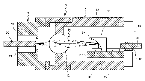
Fig. 2 schematically illustrates a vertical sectional view of the
light receiving element module 3 for explaining a light receiving
CA 02492785 2009-11-03
28964-102
8
principle of the light receiving element module 3 of Fig. 1. Fig. 2
illustrates a structure of Figs. 8A and 8B described later in a simplified
manner, where illustration of some portions is omitted and some
portions are illustrated in simplified manner.
As illustrated in Fig. 2, the light receiving element module 3
includes a stem 10 which a signal pin 40 (corresponds to signal pins
41a and 41b, ground pins 42a and 42b, and voltage supplying pins 43a
and 43b) penetrates, a base 11 fixed to the stem 10 in a direction
perpendicular thereto, a cap member 13 which has a light
passing-through hole 14 and is fixed to the stem 10, and a spherical
lens 12 which condenses signal light emitted from the optical fiber 20.
Further, the light receiving element module includes a parabolic mirror
16 which is disposed on the base 11 and reflects the signal light
condensed by the spherical lens 12 approximately at a right angle, a
light receiving element 18 which is disposed on the base 11 and
receives the signal light reflected by the parabolic mirror 16 to convert
the same to an electric signal, a trans-impedance amplifier 19 which is
disposed on the base 11 in proximity to the light receiving element 18
and amplifies the electric signal converted by the light receiving
element 18 and the like. With the light receiving element 18, a
photodiode is used in this embodiment.
The signal pin 40 penetrates the stem 10 via a dielectric 60
(corresponding to dielectrics 61, 63a, and 63b), and the base 11 and
the cap member 13 are fixed to the stem 10 in a direction perpendicular
thereto. The light receiving element 18, the parabolic mirror 16 and
CA 02492785 2005-01-11
9
the trans-impedance amplifier 19 are put on the base 11 in proximity to
one another. The light passing-through hole 14 for inserting the
spherical lens 12 is formed in the cap member 13, and the spherical
lens 12 is inserted into the light passing-through hole 14 of the cap
member 13 so that a sealed structure of the interior of the cap member
can be achieved. The spherical lens 12 can be constituted by, for
example, an inexpensive BK7 (having a reflection index of 1.51: Trade
Name of Shot Inc.). Further, the receptacle 2 formed with an insertion
hole 22 for inserting the ferrule 21 is fixed to the cap member 13. The
parabolic mirror 16 has a reflecting surface 16a, and it is arranged such
that the signal light condensed by the spherical lens 12 is incident on a
portion of the parabolic face (the reflecting surface) which is offset from
a rotation symmetry axis at a distance corresponding to about a radius.
Incidentally, the radius used here means a radius of curvature of the
parabolic face described later.
A transmission route of signal light emitted from the optical fiber
will be explained next. Signal light emitted from the optical fiber 20
is incident on the spherical lens 12. The spherical lens 12 condenses
incident signal light. A principal ray of the signal light condensed by
20 the spherical lens 12 is incident on the reflecting surface 16a generally
in parallel to the rotation symmetry axis of the reflecting surface 16a of
the parabolic mirror 16. The incident signal light is reflected generally
at a right angle on the reflecting surface 16a of the parabolic mirror 16
to be incident on the light receiving element 18. The signal light is
condensed by the reflection due to the characteristic of the parabolic
CA 02492785 2009-11-03
= 28964-102
mirror 16. The light receiving element 18 converts incident signal light
to an electric signal to output the same to the trans-impedance amplifier
19. In the trans-impedance amplifier 19, the electric signal from the
light receiving element 18 is amplified, is outputted through the signal
5 pin 40 to an external upper system. Thus, according to the light
receiving element module of the present invention, two-stage
condensation is performed at the spherical lens 12 and the parabolic
mirror 16.
The arrangement of the optical fiber 20, the spherical lens 12,
10 the parabolic mirror 16, and the light receiving element 18 will be
explained briefly. A virtual image of a light receiving face (a photo
detector, (hereinafter, "PD") light receiving face) of a light receiving
element is formed on an optical axis of signal light emitted from the
optical fiber. On the other hand, a portion (hereinafter, "an emitting
point") of the optical fiber from which a signal light is emitted is
arranged on an object point, and a real image is imaged at the imaging
point of the optical fiber on the optical axis of the signal.Iight by the
spherical lens. At this time, the optical fiber 20, the spherical lens 12,
the parabolic mirror 16 and the light receiving element 18 are arranged
such that the position of the real image of the emitting point of the
optical fiber is imaged on the position of the virtual image of the light
receiving face. That is, the virtual image is formed on the light
receiving face of the light receiving element by the reflecting mirror on
the optical axis of the lens, and the lens transfers the light emitting
point of the optical fiber placed at the object point to the virtual image
CA 02492785 2009-11-03
28964-102
11
plane of the light receiving face of the light receiving element. In other
words, such a constitution can be employed that a fiber image is formed
on the optical axis of the lens, and the fiber image is transformed to the
light receiving face of the light receiving element by the parabolic mirror.
A specific design example of the spherical lens 12 and the
parabolic mirror 16 will be explained next with reference to Fig. 3 to Figs.
7A
and 7B. The magnification of the spherical lens 12 will be first explained
using Fig. 3 to Fig. 5. Fig. 3 is a diagram for explaining spreading of a
Gaussian beam, and Fig. 4 and Fig. 5 illustrate diagrams for explaining
various symbols.
Supposing an ideal lens, a spot radius ao2 of an image, where an
optical fiber with a spot radius w1 which is located on an object point
and emits light with a wavelength X, is on an image plane defocused
from a paraxial image point by a distance z via an ideal lens of a lateral
magnification m, can be expressed by the following equation (1).
~.z
C02 (z)=mw1 1+ 2 ... (1)
~(mwi)
Fig. 3 illustrates spot radiuses on an image plane between the
paraxial image point and the defocus from 0 to 60 micrometers obtained
via an ideal lens with a lateral magnification of 0.5 to 1 for each 10
micrometers regarding an optical fiber with a wavelength of 1.3
micrometers and a spot radius of 5 micrometers utilizing the equation
(1). Since the Gaussian beam outside about 1.5 times a spot radius (a
light intensity of 1/e2) causes loss of about 2%, a spot radius of 7.5
micrometers or less to the light receiving element with a radius of 10
CA 02492785 2009-11-03
28964-102
12
micrometers used for light transmission of 10 Gb/s satisfies a suitable
condition. Incidentally, introductory remarks in Fig. 3 mean a lateral
magnification and a defocus amount (millimeter). That is, for example,
co2 (m, 60X10"3) means a spot radius (co2) obtained when the lateral
magnification is m times and the defocus amount is 60 micrometers.
When considering, for example, a thickness tolerance of 30
micrometers from Fig. 3, it is understood that the lateral magnification
of 0.7 is optimal, however, the lateral magnification of about 1 is excellent
in an
optical system having a large optical axis shift (for example, of the
defocus amount of 60 micrometers) and so on. Practically, considering
an image blur due to the aberration of the optical system and an
assembling tolerance, the lateral magnification of the whole optical
system is set to a range of 0.5 to 1.
The optical system including the lens 12 and the parabolic
mirror 16 will be explained next with reference to Fig. 4. In Fig. 4, it is
assumed that the lens 12 is an ideal lens 120 with a focal length f1 and
the parabolic mirror 16 has a reflecting surface 16a constituting a
paraboloid 16 with a radius of curvature r in the vicinity of a rotation
symmetry axis z. The parabolic face 16 is a paraboloid of z = y2/2r to
an axis y perpendicular to the optical axis, and a principal ray from the
lens is incident on a position (a point R) of the height h from the rotation
symmetry axis and is reflected. An inclination of a principal ray
generated in a manner shifted from the optical axis by S is defined as u,
a crossing point between a ray reflected at a time of u = 0 and the
rotation symmetry axis is defined as a point Q, an angle formed
CA 02492785 2005-01-11
13
between the reflected beam and y axis is defined as 0, and the position
where the point Q is shifted by b' at a time of angle u is defined as Q'.
According to the paraxial and coaxial optical system, it is assumed that
the magnification is defined as y = b'/b in the optical system of Fig. 4.
Since b=f, tan u, RQ'= h, and b'=RQ . sinu _ hsinu is obtained from
cos B cos 9 cos z B
Fig. 4, the magnification is obtained by the following equation.
h sinu 1 h 1 (2)
Y f l tan u cos z 9 f, cos ` fI
z
Since the paraboloid is z= y , the angle 0 can be obtained from
2r
r h2
tan0= 2 2r
h
According to the equation (2), it will be understood that the
magnification y is influenced by the position h on the paraboloid 16
upon the principal ray is incident. When such a usage is applied, the
parabolic mirror 16 may be used in the vicinity of h;:z, r for reducing
aberration, and it can be thought that the focal length is f2=r, and a
principal plane is a plane including R point at which the principal ray is
incident upon the reflecting mirror.
A partial system of an optical system constituting the parabolic
mirror 16 with reference to Fig. 5. Considering that the parabolic
mirror 16 is an ideal lens 162 with a focal length f2, and assuming that
a spot radius formed on a light receiving face of the light receiving
element is copd, a space between the light receiving face and the
CA 02492785 2009-11-03
28964-102
14
principal plane is dO, a spot radius of a virtual image is copd', and the
distance between the virtual image and the principal plane is dl (which
is a virtual image and takes a negative number), the lateral
magnification m2 of the partial system and dl can be expressed by the
following equations.
( ,
,
m'- - ~m ,~ ~.f, ) +lI 1- f. (3)
,
2
~0 10 2
( .fz ) ' -d o (]-'
f J
~ d,= nTU (4)
Z 2 Z d ~
.f2 J 1 f
Fig. 6A illustrates a lateral magnification m2 of the partial
system corresponding to the distance dO showing the space between
the principal plane and the light receiving face (PD light receiving face)
18a of the light receiving element 18 regarding the parabolic mirror 16
having a parabolic face with a radius r varying from 0.55 millimeters to
0.95 millimeters. Further, Fig. 6B illustrates the virtual image position
dl versus the distance dO regarding the reflecting mirror having the
paraboloid 16 with the radius r varying from 0.55 millimeter to 0.95
millimeter. Incidentaily, introductory remarks in *respective diagrams of
Figs. 6A and 6B mean the radius (millimeters) of the paraboloid of the
parabolic
mirror 16 and the space (millimeters) between the principal plane and
the light receiving face (PD light receiving face) 18a of the light
receiving element 18. That is, for example, m2 (0.55, dO) means the
lateral magnification (m2) when the radius is 0.55 millimeter and the
CA 02492785 2009-11-03
28964-102
space between the principal plane and the PD light receiving face is dO.
For simple example, assuming that the lateral
magnification m of the entire optical system is one time and the lateral
magnification m2 of the partial system obtained by the reflecting mirror of
5 the parabolic face 16 is 0.5 times, the distance between the point R
(principal plane) and the PD light receiving face 18a varies from 0.28
millimeter to 0.48 millimeter according to variation of the radius r of the
reflecting mirror having the paraboloid 16 from 0.55 millimeter to 0.95
millimeter, which is suitable for keeping ttie height of the rising portion
10 of a wire bond used for wiring of the light receiving element 18, so that
the wire bond and the reflecting mirror face of ttie parabolic mirror 16
must not come in contact with each other.
A partial system of the spherical lens 12 wili be explained next.
A first lens on which light emitted from the optical fiber 20 is incident is
15 a spherical lens 12 with a radius R and a refractive index n, and its
focal length is f1 = R/(2(n - 1)). A ray trace in Fig. 2 illustrates a
diagram where 11 rays have been traced in a range of NA 0.2 for each
NA 0.04, where a ray with NA 0.16 and a ray with NA 0.2 cross. In this
manner, the spherical lens 12 is inexpensive, however, its spherical
aberration is large. Decrease in the lens power (a refractive power)
decreases the aberration, and the lateral magnification of the partial
system of the lens is then designed about two times. In this connection,
since NA of the optical fiber for the wavelength of 1.3 micrometers is 0.1
and the spot radius is 5 micrometers at an intensity
CA 02492785 2009-11-03
28964-102
16
of 1/e2, a light intensity distribution of about 98% can be included within
NA of 0.15, and blur of an image is very small with such optical design
noted above.
Incidentally, for example, assuming the reflecting mirror of the
parabolic mirror 16 is a flat mirror and aberration is achieved by an
finite system including one lens, even assuming a preferable lateral
magnification is about 0.8 to 0.9 or so, a shading loss to a light
receiving radius of 10 micrometers becomes large as about 5%.
Therefore, the lateral magnification of the partial system of the lens is
preferably designed one time or more.
The constitution of the parabolic reflecting mirror will be
explained next. A hyperbolic reflecting mirror can achieve an aplanatic
condition in the optical system
illustrated in Fig. 2, and a parabolic reflecting mirror (the parabolic
mirror 16) can achieve an aplanatic condition when it converges a
collimated beam. However, the parabolic reflecting mirror has a merit
that its rotation symmetry axis and its optical axis are parallel to each
other, a merit that forming molds can be manufactured by a mirror
finishing lathe with a high cutting accuracy instead of a mirror finishing
milling machine for manufacturing an oval surface or a hyperboloid, and
a merit that assembling of the forming molds can be made easy
because there are the rotation symmetry axes in the forming molds.
A coefficient of thermal expansion a of plastic suitable for
manufacturing a parabolic reflecting mirror (the parabolic mirror 16) is
5.6 x 10"5. For example, a movement of the reflecting point (R point)
CA 02492785 2009-11-03
28964-102
17
from a bottom of the reflecting mirror is about 2.5 micrometers when a
parabolic mirror with a radius r of 0.85 millimeters is used with lateral
magnification of 0.5 and the temperature varies from 25 C to 85 C,
assuming that a space between a reflecting point (R point in Fig. 4) and
a light receiving face (the PD light receiving face) 18a of the light
receiving element 18 is 450 micrometers, the thickness of a light
receiving element 18 is 150 micrometers, and the thickness of a
substrate (a chip carrier) for a light receiving element 17 made of
ceramic is 145 micrometers. On the other hand, focal point change is
small because of the longitudinal magnification of 0.25, though the focal
length change of the parabolic mirror is 2.8 micrometers. Similarly,
when the radius is 1 millimeter or less and the lateral magnification of
the.partial system of the parabolic reflecting mirror is one time or less,
blur of an image due to a temperature change of the image point is
reduced, and a suitable optical system can be obtained with a simple
structure.. without arranging the image point compensation unit with a
complicated structure described in Japanese Patent Publication No.
2907203.
The merits of the optical system are further explained with
reference to Figs. 7A and 7B. As illustrated in Fig. 2, the lens
12 is mounted in the cap 13, and the cap 13 is welded on the stem 10
so as to attain an air-tight structure by such a method as a projection
welding. However, it is relatively difficult to secure position accuracy in
the welding step. For example illustrated in Fig. 7A, if the
misalignment A between the reflecting point R of the parabolic mirror 16
CA 02492785 2009-11-03
28964-102
18
and the central axis of the lens 12 takes place when the welding is
performed, decrease in the light receiving sensitivity about 2% when the
misalignment A is 100 micrometers as shown in Fig. 7B due to the
optical fiber 20 alignment 0/m1 from the lens center 12, and also proper
adjustment g between the lens principal plane and the fiber 20, where
the ml is lateral magnification of the partial system of the lens. With
such a constitution, when the optical fiber 20 or the receptacle 2 is
adjusted properly in the optical axial direction and a direction
perpendicular to the optical axis, misalignment of respective parts are
compensated for, so that a suitable optical coupling can be obtained.
A detailed constitution of the light receiving element module 3 of
Fig. 1 will be explained next. Figs. 8A and 8B illustrate a horizontal
sectional view and a vertical sectional view of the light receiving
element module 3 of Fig. 1. As illustrated in Figs. 8A and 8B, the light
receiving element module 3 is provided with a disc-like stem 10 mounted with
signal pins 41a and 41b constituted differential feed, a supplying pin
43a for a bias voltage to a photodiode 18, a supplying pin 43b for a
power source voltage to the trans-impedance amplifier 19, ground pins
42a and 42b and the like, a trapezoidal column-shape base 11 mounted
with a parabolic mirror 16 and a plurality of elements, a spherical lens
12 for condensing signal light emitted from the optical fiber 20, a
cylindrical cap member 13 for sealing the base 11 and the like from the
outside, a receptacle 2 in which a ferrule 21 connected with the optical
fiber 20 is inserted, and the like.
The cap member 13 exhibits a two-stage cylindrical shape so as
CA 02492785 2005-01-11
19
to include a first cap member 13a fixed to the stem 10 by projection
welding or the like and a second cap member 13b fitted on a distal end
of the first cap member 13a and fixed to the first cap member 13a by
YAG welding or the like.
A light passing-through hole 14 for insertion of the spherical lens
12 is formed at a distal end of the first cap member 13a, and the
spherical lens 12 is inserted into the light passing-through hole 14.
The spherical lens 12 is constituted with, for example, BK7 (a refractive
index of 1.51), and it is fixed to the first cap member 13a by solder
glass with a low melting point. An inner space 15 of the first cap
member 13a is isolated by the spherical lens 12 from the outside, so
that the inner space 15 in which the base 11 is accommodated is
maintained in an air-tight state.
By positioning and adjusting the second cap member 13b in a
direction in which the ferule 21 (refer to Fig. 2) is inserted (in an optical
axial direction) to fix the same to the first cap member 13a, alignment
between the spherical lens 12 and the optical fiber 20 inserted into the
receptacle 2 in the optical axial direction is performed.
The receptacle 2 has a ferule insertion hole 22 in which the
ferule 21 connected with the optical fiber 20 and a light passing-through
window 23 for allowing passing-through of signal light emitted from the
optical fiber 20. The receptacle 2 is fixed to the second cap member
13b by YAG welding or the like. When the receptacle 2 is fixed to the
second cap member 13b, positioning between the spherical lens 12 and
the optical fiber 20 mounted to the receptacle 2 regarding two directions
CA 02492785 2009-11-03
28964-102
perpendicular to the optical axis is aligned by conducting positioning
and adjusting in the two directions perpendicular to the optical axis.
Thus, when the second cap member 13b and the receptacle 2 are fixed,
they are positioned and adjusted, so that adjustment in three axial
5 directions to the optical axis is performed.
The ferrule 21 connected with the optical fiber 20 has a proper
mechanism (not illustrated) for, when the ferrule 21 is inserted into the
ferrule insertion hole 22 of the receptacle 2, pressing the ferrule 21 to
lock and fix the ferrule 21 to the receptacle 2.
10 The constitution of the interior of the can package 1 will be
explained next. Figs. 9A and 9B illustrate arrangement relationship among the
stem 10, the pins and the base 11. As illustrated in Figs. 9A and 9B, the can
package I is constituted with a disc-like stem 10 mounted with a
plurality of pins and a trapezoidal column-like base 11 fixed to an inner
15 wall face of the stem 10 in a perpendicular direction thereto by Ag
brazing or the like.
The stem 10 constituting a ground is mounted with a pair of
signal pins 41a and 41b constituted differential feed for signal
transmission of the light receiving element 18, two ground pins 42a and
20 42b placed on both sides of the signal pins 41 a and 41b, and voltage
supplying pins 43a and 43b for supplying a power source voltage of the
trans-impedance amplifier 19 and supplying a bias voltage to the light
receiving element 18.
The signal pins 41a and 41b and the ground pins 42a and 42b
constitute a field-through which penetrates the stem 10. These
CA 02492785 2009-11-03
28964-102
21
respective signal pins are fixed to the stem 10 in an air-tight sealing
state via dielectrics (61, 63a, and 63b) formed from material such as
glass. The ground pins 42a and 42b are fixed to an outer wall face
10z of the stem 10 constituting the ground by pressure-fitting and
welding.
In further detailed explanation, the stem 10 is formed of metal
such as kovar (Fe - Ni alloy), soft iron or CuW (copper tungsten), and
plating of Ni, gold or the like is ordinarily performed on an upper layer
of the stem. Further, for example, in case of kovar (Fe - Ni alloy) or
soft iron, the stem 10 can be manufactured by punching out a metal
plate thereof by a die. For example, in the case of CuW, the stem can
be manufactured using a metal injection molding technique, and the
manufacturing cost is inexpensive because of the process is simple.
The stem 10 is laid out with a plurality of holes 51, 53a and 53b, and
dielectrics 61, 63a, and 63b are respectively inserted into these holes
51, 53a and 53b.
A pair of pin insertion holes (reference numerals are omitted)
are formed in the dielectric 61, and the signal pins 41a and 41b are
inserted and fixed in these pin insertion holes. Similarly, holes
(reference numerals are omitted) are respectively formed in the
dielectrics 63a and 63b, and voltage supplying pins 43a and 43b are
inserted and fixed in the respective holes. The shape of the dielectric
61 in which the pair of signal pins 41a and 41b are inserted is an elliptic
shape in this case. Correspondingly, the hole 51 in which the dielectric
61 is inserted is also an elliptic shape. The other dielectrics 63a and
CA 02492785 2009-11-03
28964-102
22
63b are formed in a circular shape. Incidentally, the ground pins 42a
and 42b do not penetrate the stem and are fixed to the outer wall face
lOz of the stem 10 by pressure-fitting and welding, as described above.
As the dielectrics 61, 63a, and 63b, for example, kovar glass
(soda barium glass), boro-silicated glass or the like is used. Further,
as the signal pins 41 a and 41 b, the voltage supplying pins 43a and 43b,
and the ground pins 42a and 42b, for example, such a metal as kovar,
50% Ni - Fe alloy or the like is used.
When the stem 10 and the base 11 are manufactured as
separate members from each other, the base 11 is connected and fixed
to the stem 10 by Ag brazing or the like. Of course, the stem 10 and
the base 11 may be manufactured as an integral member.
A differential line substrate 31, a trans-impedance amplifier
circuit element 33, a light receiving element circuit element 32, a
trans-impedance amplifier 19, a parabolic mirror 16, and a light
receiving element substrate 17 are mounted on an upper face of the
base 11. When a capacitor of a ceramic chip type is used as the
substrate 17 for a light receiving element, connection with the light
receiving element is achieved by soldering fixation so that inductance
can be reduced and resonance due to wiring with the trans-impedance
amplifier 19 or the like can be prevented, which is preferable. The
base 11 constitutes a whole ground conductor layer (hereinafter, "solid
ground") by plating, and the solid ground is connected to a ground
formed on a back face of each element as flat conductor plates.
The differential line substrate 31 includes a pair of differential
CA 02492785 2005-01-11
23
microstrip lines 31 a and 31 b formed symmetrically, and a solid ground
(not illustrated) formed on a back face of the substrate. One ends of
the differential microstrip lines 31 a and 31 b are formed with a pair of
pads (91 a and 91 b), wider portions 92, and stubs 93a and 93b for
taking impedance matching with a field-through portion and front side
and rear side circuits. End portions of the signal pins 41 a and 41 b
mounted on the stem 10 are connected and fixed to the pads of the
differential line substrates 31 by brazing or soldering.
The light receiving element circuit element 32 is mounted with a
circuit element (a capacitor, a resistance, a coil or the like) for
eliminating noises in a certain frequency band when a bias voltage is
applied to the light receiving element 18 mounted on the substrate 17
for a light receiving element. The light receiving element circuit
element 32 is formed with a plurality of pads (reference numerals are
omitted), it is connected to the voltage supplying pin 43a via a wire
bond 95a and is connected to a pad of the light receiving element
substrate 17 via another wire bond 70c.
A trans-impedance amplifier circuit element 33 is mounted with a
circuit element (a capacitor, a resistance, a coil or the like) for
eliminating noises in a certain frequency band of a power source
voltage supplied to the trans-impedance amplifier 19. The
trans-impedance amplifier circuit element 33 is formed with a plurality of
pads (reference numerals are omitted), and it is connected to the
voltage supplying pin 43b via a wire bond 95b and is connected to the
pad of the trans-impedance amplifier 19 via a wire bond 70d.
CA 02492785 2009-11-03
28964-102
24
An output terminal for a differential signal from the
trans-impedance amplifier 19 is connected to pads of the differential
line substrate 31 and the like via wire bonds 96a and 96b. Further, the
trans-impedance amplifier 19 is connected to pads of the light receiving
element 18, the light receiving element circuit element 32 and the like
via wire bonds (which will be described later in explanation regarding
Figs. 10A to 10C). The trans-impedance amplifier 19 performs
current/voltage conversion on an electric signal inputted from the light
receiving element 18 to amplify the same.
The light receiving element substrate 17 is mounted with a light
receiving element 18 such as, for example, a pin-type photodiode, and
it is formed with a plurality of pads (reference numerals are omitted)
and is connected to the light receiving element circuit element 32 and
the trans-impedance amplifier 19 via wire bonds. The light receiving
element 18 receives signal light reflected by the parabolic mirror 16 to
convert it to an electric signal (a monitor signal). After the electric
signal is amplified by the trans-impedance amplifier 19, the amplified
signal is outputted from output terminals for a differential signal in the
trans-impedance amplifier 19, and outputted from the signal pins 41a
and 41b mounted on the stem 10 via a pair of differential data lines 31a
and 31b of the differential line substrate 31 to an upper system.
The parabolic mirror 16 is formed in a plastic mold. As
illustrated in Figs. 8A and 8B, the parabolic mirror 16 has a reflecting
surface
16a shaping a paraboloid, and it is formed with a groove (refer to Figs. 10A
to 10C) for connecting the light receiving element 18 and the trans-impedance
CA 02492785 2009-11-03
28964-102
amplifier 19 via a wire bond. The reflecting surface 16a is given with a
base film with an excellent adhesion such as chromium and then
applied with such a metal film as gold, aluminum, silver with a high
reflectivity using such a method as electron beam vapor deposition or
5 sputtering. Further, the reflecting film may be one where dielectric
multi-layer of titanium dioxide or silicon dioxide, or alumina or tantalum
pentoxide has been used, or it may be one where a protective film of
dielectric has been applied on a metal film. Incidentally, an effect for
prevention of short-circuiting with a wire bond can be achieved by
10 applying an insulating film on a surface of the reflecting surface 16a,
which is preferable.
The reflecting surface 16a of the parabolic mirror 16 serves to
reflect signal light condensed by the spherical lens 12 at an angle of
about 900 to reach the
15 light receiving face 18a of the light receiving element 18, and the
reflecting surface 16a is formed in a parabolic shape, so that aberration
is hardly generated and the responsivity of the light receiving element
18 can be increased.
By reflecting a raypath of signal light at almost a right angle by
20 the parabolic mirror 16 in this manner, it is made possible to arrange
the spherical lens 12 and various electric parts at a position horizontal
direction to the surface of the light receiving element 18, and it is made
possible to reduce the thickness of the light receiving element module.
Figs. 10A to 10C are diagrams for explaining electric connection
25 of the light receiving element 18 and the trans-impedance amplifier 19,
CA 02492785 2009-11-03
28964-102
26
wherein Fig. 10A is a vertical sectional view of the periphery of the
parabolic mirror 16, Fig. 10B is a front view, and Fig. 10C is a plan
view when the parabolic mirror 16 has been removed. As illustrated in
Figs. 10A to 10C, the light receiving element 18 and the
trans-impedance amplifier 19 are mounted on one flat face of the base
11 in proximity to each other. The light receiving element 18 mounted
on the light receiving element substrate 17 includes a photodiode of a
surface incident type having a light receiving face on a surface side,
and a light receiving face (a photodiode portion) 18a and a pad 18b (for
example, a p-side electrode) which is an electrode are formed on the
surface side. Further, an electrode (for example, an n-side electrode)
is formed on the side of the light receiving element substrate 17.
A groove 16b for connecting the light receiving element 18 and
the trans-impedance amplifier 19 by a wire bond is formed on the
parabolic mirror 16. Incidentally, the groove 16b has a semi-cylindrical
shape in, the drawing, but it is not limited to this shape. For example,
the groove may have a rectangular parallelepiped shape. That is., if
the groove penetrates the parabolic mirror 16 like a tunnel in a state
that the parabolic mirror 16 has been mounted on the base 11, it can
take any shape. A pad 19b for inputting an electric signal and a
ground 19a are formed on the trans-impedance amplifier 19. A pad
18b on an anode side of the light receiving element 18 and the pad 19b
of the trans-impedance amplifier 19 are respectively bonded to one end
side and the other end side of a wire bond 70b. An electrode (not
illustrated) on a cathode side of the light.receiving element 18 is
CA 02492785 2009-11-03
28964-102
27
soldered an electrode 17a of the light receiving element substrate 17.
An electrode 17a of the light receiving element substrate 17 is
connected to a light receiving element circuit element 32 via a wire
bond 17c, and the light receiving element circuit element 32 is
connected to a voltage pin 43a. An electrode on a back face of a
capacitor 32b is connected to the electrode 17a of the light receiving
element substrate 17. An electrode on a surface of the capacitor 32b
is connected to a ground face 17b of the light receiving element
substrate 17 via a wire bond 70e. Further, an electrode on a surface
of the capacitor 32b is connected to the ground 19a of the
trans-impedance amplifier 19 via a wire bond 70a. The ground face
17b of the light receiving element substrate 17 is connected to a
surface (a ground face) of the base 11 via a through hole 17c.
Figs. 11A to 11 C are diagrams for explaining electric connection
of the light receiving element 18 and the trans-impedance amplifier 19,
wherein, as another example of Figs. 10A to 10C, Fig. 11A is a vertical
sectional view of the periphery of the parabolic mirror 16, Fig. 11 B is a
front view and Fig. 11 C is a plan view when the parabolic mirror 16
has been removed. As illustrated in Figs. 11A to 11C, a structure may
be simplified by using a parallel flat-plate capacitor 170 of a ceramic
chip type instead of the light receiving element substrate 17. In this
case, a back face of the light receiving element 18 is mounted on an
upper face of the capacitor 170 of a ceramic chip type and the back
face of the capacitor 170 of a ceramic chip type is connected to a
ground face of the base 11. That is, flat faces of electrodes at both
CA 02492785 2009-11-03
28964-102
28
ends of the capacitor 170 are made parallel, fixation is made such that
the electrode at a lower end of the capacitor 170 is electrically
connected to the ground face of the base 11, and placement is made
such that the electrode at an upper end of the capacitor 170 is
electrically connected to the electrode at a back face side of the
photodiode. Further, the ground 19a of the trans-impedance amplifier
19 is connected to the ground face of the base 11 in the same manner
as Figs. 10A to 10C. Furthermore, the pad 19b of the trans-impedance
amplifier 19 is connected to the pad 18b of the light receiving element
18.
According to the light receiving element module of the first
embodiment, since such a constitution is employed that signal light
emitted from the optical fiber 20 is condensed by the spherical lens 12
and the condensed signal light is reflected by the parabolic mirror 16,
the region of the reflecting surface 16a of the parabolic mirror 16 can be
made small, and the parabolic mirror 16 can be reduced in size.
Thereby, it is made possible to reduce the light receiving element
module in size. Furthermore, influence of a thermal expansion
coefficient due to material for the reflecting mirror is reduced and
structure is simplified.
Further, since the parabolic mirror 16 is constituted so as to
reflect signal light to an approximately right angle at a position
approximately offset from the center of the paraboloid by an
approximately half radius and to incident the signal light to the light
receiving element 18, aberration due to the parabolic face (the
CA 02492785 2009-11-03
28964-102
29
reflecting surface) of the parabolic mirror 16 can be decreased and
image blur can be reduced.
Furthermore, since such a constitution is employed that signal
light is condensed by the spherical lens 12 and the parabolic face of the
parabolic mirror 16, it is made possible to reduce the refractive power
due to the spherical lens 12 to reduce image blur due to the spherical
aberration.
Moreover, since use of three-axis alignment in the fixing process
of the second cap member 13b and the receptacle 2, an image of signal
light can be accurately positioned to the light receiving face 18a of the
light receiving element 18.
In addition, since the light receiving element 18 and the
trans-impedance amplifier 19 are mounted on the base 11 in proximity
to each other, it is made possible to improve a high frequency
characteristic.
Further, by using the capacity of the ceramic chip type on the
light receiving element substrate 17, it is made possible to prevent
resonance owing to inductances of wire bonds 70a and 70b connecting
the light receiving element 18 and the trans-impedance amplifier 19.
Since the light passing-through hole 14 in which the spherical
lens 12 is inserted is formed in the cap member 13 and a sealed
structure is realized by inserting the spherical lens 12 into the light
passing-through hole 14, the reliable sealed structure can be realized
inexpensively.
In this connection, in the first embodiment, the parabolic mirror
CA 02492785 2009-11-03
28964-102
is used as a reflecting mirror having a quadric surface reflecting surface,
a hyperboloid mirror whose reflecting surface is a hyperboloid may be
used. Further, in the first embodiment, though the photodiode is used
as the light receiving element 18, another photo-semiconductor element
5 such as an avalanche photodiode can be used.
Second Embodiment
A light receiving element module of the second embodiment will
be explained with reference to Figs. 12A to 12C. In the light receiving
element
10 module of the first embodiment, the photodiode 18 of the surface
incident type is used as the light receiving element. In the light
receiving element module of the second embodiment, a photodiode 180
of a back surface incident type is used so that a groove.of the parabolic
mirror 16 for connecting the light receiving element 180 and the
15 trans-impedance amplifier 19 via a wire bond becomes unnecessary.
Figs. 12A to 12C are diagrams for explaining electric connection of the light
receiving element 180 and the trans-impedance amplifier 19, wherein
Fig. 12A is a vertical sectional view of the periphery of the parabolic
mirror 16, Fig. 12B is a front view and Fig. 12C is a plan view where
20 the parabolic mirror 16 tias been removed. In Figs. 12A to 12C, like
reference numerals are designated to portions having functions
equivalent to those in Figs. 10A to 10C.
As illustrated in Figs. 12A to 12C, a light receiving element 180
mounted on a light receiving element substrate 175 includes a photodiode
25 of a back face incident type having a light receiving face on a back face,
CA 02492785 2009-11-03
28964-102
31
and a light receiving face (a photodiode portion) 180a is formed on the
back face side. A pair of electrodes 175a and 175c (a pair of p-side
and n-side electrodes) are formed on surface side of the light receiving
element substrate 175. A pair of unillustrated terminals (an anode and
a cathode) of the light receiving element 180 are respectively
connected to the electrodes 175a and 175c of the light receiving
element substrate 175 by soldering. Further, a back surface electrode
of a capacitor 32b is soldered on an upper face of the electrode 175a.
A surface electrode of the capacitor 32b is connected to another
conductor pad 175b of the light receiving element substrate 175. The
conductor pad 175b is connected to a surface of the base 11 via a
through hole 175e. One end of a wire bond 70a is bonded to another
conductor pad 175d of the light receiving element substrate 175, and
the other end of the wire bond 70a is connected to a pad 19a of the
trans-impedance amplifier 19. The surface electrode of the capacitor
32b is also connected to a conductor pad 175d of the light receiving
element substrate 175. One end of a wire bond 70b is connected to an
electrode 175c and the other end of the wire bond 70b is bonded to a
pad 19b of the trans-impedance amplifier 19.
According to the light receiving element module of the second
embodiment, since the photodiode of the back face incident type is
used as the light receiving element 180, it is made unnecessary to
provide the groove 16b (refer to Figs. 10A to 10C) of the parabolic mirror 16
for connecting the light receiving element 180 and the trans-impedance
amplifier 19 via a wire bond, so that working for the groove 16b of the
CA 02492785 2009-11-03
28964-102
32
parabolic mirror 16 is made unnecessary and manufacturing cost of the
parabolic mirror 16 can be reduced.
Third Embodiment
A light receiving element module of the third embodiment will be
explained with reference to Fig. 13. In the light receiving element
module of the first embodiment, the trans-impedance amplifier 19 is
arranged on a rear stage side of the light receiving element 18 on the
base 11. In the light receiving element module of the third embodiment,
the trans-impedance amplifier 19 is arranged on a front stage of the
light receiving element 18 on the base 11, so that space saving in a
widthwise direction (a horizontal direction) of the light receiving element
module 3 is achieved. Fig. 13 schematically illustrates a vertical
sectional view of the light receiving element module 3 of Fig. 1, where
some portions are omitted and some portions are illustrated in a
simplified manner. In Fig. 13,1ike reference numerals are designated
to portions having functions equivalent to those in Fig. 2. As illustrated
in Fig. 13, the trans-impedance amplifier 19 is arranged on a front stage
side of the light receiving element 18 and the parabolic mirror 16 is
arranged on a rear stage side of the light receiving element 18. At this
time, the parabolic mirror 16 is provided to the strip differential data
lines 31a and 31b such that the differential microstrip lines 31a and 31b
do not interfere with the light receiving element 18.
According to the light receiving element module of the third
embodiment, since the trans-impedance amplifier 19 is arranged on the
CA 02492785 2009-11-03
28964-102
33
front stage side of the light receiving element 18 on the base 11, it is
made possible to save a space in the widthwise direction (a horizontal
direction) of the light receiving element module by a space for arranging
the trans-impedance amplifier 19, as compared with the light receiving
element module of the first embodiment.
Furthermore, the wire bonds 70a and 70b for connecting the
trans-impedance amplifier 19 and the light receiving element 18 can be
arranged ahead of the parabolic mirror 16 (on the side of the optical
fiber 20), and the trans-impedance amplifier 19 and the light receiving
element 18 can be connected to each other unless the groove 16b as
shown Figs. 10A to 10C.
Fourth Embodiment
A light receiving element module of the fourth embodiment will
be explained with reference to Fig. 14. In the (ight receiving element
module of the first embodiment, the sealed structure is formed by
inserting the spherical lens 12 into the light passing-through hole
formed in the cap member 13. In the light receiving element module of
the. fourth embodiment, a sealed structure is formed by arranging a
transparent member in the light passing-through hole formed in the cap
member 13. Fig. 14 schematically illustrates a vertical sectional view
of the light receiving element module of Fig. 1, where some portions are
CA 02492785 2009-11-03
28964-102
34
omitted and some portions are illustrated in a simplified manner. In
Fig. 14, like reference numerals are designated to portions having
functions equivalent to those in Fig. 2.
A lens holding member 80 which holds the lens 12 is provided
between the receptacle 2 and the cap member 13. An end face of the
lens holding member 80 is joined to one end face of the cap member 13
on the side of a light passing-through hole 81 by welding or the like.
Further, an outer periphery of the lens holding member 80 is fitted into
an inner periphery of a connection member 85 on its one end side, and
the connection member 85 is slid to the lens holding member 80 and
welded thereto. An end face of the connection member 85 on the
other end is welded to an end face of the receptacle 2 opposed to the
hole 22 thereof.
As illustrated in Fig. 14, a light passing-through hole 81 is
formed in the cap member 13, and the light passing-through hole 81 is
covered with. a transparent member (a window member) 82 which is
formed of.cover glass or the like and is fixed to an inner wall of the cap
member 13 formed with the light passing-through hole 81 by a solder
glass or the like. A sealed structure is achieved by the
transparent member 82. The lens holding member 80 which is
cylindrical shape and where a light passing-through hole for inserting
the spherical lens 12 is formed is fixed to the cap member 13. The
spherical lens 12 is inserted into the light passing-through hole and
fixed therein by adhesive or the like. Further, the receptacle 2 is fixed
in the lens holding member 80.
CA 02492785 2009-11-03
28964-102
According to the light receiving element module of the fourth
embodiment, since the sealed structure is realized by fixing the
transparent member 82 to the inner wall side of the cap member 13
formed with the light passing-through hole 81 to cover the light
5 passing-through hole 81, the sealed structure can be realized
inexpensively and it is made possible to realize a reliable sealed
structure.
It should be noted that the present invention is not limited to the
embodimcnts described above, and various modifications may be
10 embodied without changing the gist of the invention.
As explained above, according to the present invention, since
the light receiving element module is constituted so as to includes a
lens which condenses signal light emitted from an optical fiber, a
reflecting mirror which has a quadric surface reflecting surface
15 reflecting the signal light condensed by the lens, and a light receiving
element which receives the signal light reflected by the reflecting mirror
to convert the same to an electric signal, so that the region of the
reflecting surface of the reflecting mirror can be made small and the
reflecting mirror can be reduced in size. As a result, influence of a
20 thermal expansion coefficient due to material for the reflecting mirror
can be reduced and structure of the module can be simplified. Further,
it is made possible to provide an inexpensive light receiving element
module which can be reduced in size.
CA 02492785 2005-01-11
36
INDUSTRIAL APPLICABILITY
As described above, the light receiving element module
according to the present invention can be widely applied to a receiver
and a transceiver for an optical communication system using an optical
fiber.