Note: Descriptions are shown in the official language in which they were submitted.
CA 02493351 1998-12-09
1
Pb-FREE SOLDER-CONNECTED STRUCTURE AND
ELECTRONIC DEVICE
This is a division of co-pending Canadian
Patent Application.Serial No. 2,314,116 filed on
December 9, 1998.
TECHNICAL FIELD
The present invention relates to a bonded
structure by a lead-free solder, in which an electronic
device is bonded to an electrode of a lead frame, etc. by
means of the lead-free solder of low toxicity, and an
electronic article with the bonded structure.
BACKGROUND ART
In order to produce an electric circuit board
by bonding electric devices (e. g. LSIs) to a circuit
board made of an organic material, for example,
conventionally, there has been used a eutectic Sn-Pb
alloy solder, another Sn-Pb alloy solder which has a
chemical composition and a melting point each close to
that of the eutectic Sn-Pb alloy solder, and other solder
alloys which are obtained by adding small amounts of
bithmuth (Bi) and/or silver (Ag) to the solders recited
above. These solders comprise about 40 wt$ Pb and have a
melting point of about 183°C, which permit soldering at
220-240°C.
With regard to electrodes of electronic
devices, such as QFP (Quad Flat Package)-LSIs, to be
soldered, there have been usually used those made of 42
CA 02493351 1998-12-09
2
alloy which is an Fe-Ni alloy and on which a layer of
90 wt% Sn-10 wt% Pb alloy (hereinafter referred to "Sn-
lOPb") is formed. This is because such electrodes have
good wettability, good preservation and no problem of
formation of whiskers.
However, the lead (Pb) in the Sn-Pb solders
is a heavy metal harmful to humans and pollution of the
global environment caused by dumping of lead-containing
products and their bad effect on living things have
presented problems. The pollution of the global
environment by electrical appliances occurs when lead
is dissolved by rain, etc. from the dumped
lead-containing electrical appliances exposed to
sunlight and rain. The dissolution of Pb tends to be
accelerated by the recent acid rain. In order to
reduce environmental pollution, therefore, it is
necessary to use a lead-free soldering material of low
toxicity not containing lead as a substitute for the
above eutectic Sn-Pb alloy solder which is used in
large quantity and to employ a structure of the
electrode of a device not containing lead as a
substitute material to replace the Sn-lOPb layer
provided on the electrode of a device. An Sn-Ag-Bi
alloy solder is a promising candidate as a lead-free
soldering material in terms of low toxicity,
obtainability for raw materials, production cost,
wettability, mechanical properties, reliability, etc.
Soldering is usually performed at a temperature of
CA 02493351 1998-12-09
3
about 220-240°C so as to produce compounds between an
electrode of a component and a solder, and between an
electrode of a board and a solder. From this, because
the bonding interfaces differs from one another
depending upon different kinds of combinations of
solder materials and electrode materials of components,
an electrode material suitable to the respective solder
is required in order to obtain a stable bonding
interface.
An object of the present invention is to
provide a bonded structure by a lead-free-solder, in
which a lead free Sn-Ag-Bi alloy solder having low
toxicity is used for electrodes of lead frames, etc.
and which has a stable bonding interface and an enough
bonding strength.
Another object of the invention is to provide
an electronic article with utilization of a lead-free
Sn-Ag-Bi alloy solder having low toxicity, which has a
stable bonding interface with respect to a change in
process of time and a strength high enough to withstand
stress generated in bonded portions by soldering due to
a difference in thermal expansion coefficient between
electric devices and a board, a work of dividing the
board after soldering, warping of the board during the
probing test, handling and so on.
A further object of the invention is to
provide a bonded structure and an electronic article
with utilization of a lead-free Sn-Ag-Bi alloy solder
CA 02493351 1998-12-09
4
having low toxicity, which has enough bonding strength
while ensuring resistance to formation of whiskers,
wettability of the solder and so on.
DISCLOSURE OF INVENTION
In accordance with one aspect of the present
invention there is provided an electronic device
comprising a substrate and a semiconductor device both
of which are connected with each other by means of a
Pb-free solder comprising Bi, the semiconductor device
having a lead on which an Sn-Bi alloy layer comprising
1 to 20 wt$ Bi is formed.
In accordance with another aspect of the
present invention there is provided an electronic
device comprising a substrate and a semiconductor
device both of which are connected with each other by
means of a Pb-free solder comprising Bi, the
semiconductor device having a lead made of Cu or a Cu
alloy on which an Sn-Bi alloy plating layer comprising
l to 20 wt$ Bi is formed as a surface layer.
In accordance with yet another aspect of the
present invention there is provided an electronic
device comprising a substrate and a semiconductor
device both of which are connected with each other by
means of a Pb-free solder comprising Bi, the
semiconductor device having a lead made of Cu or a Cu
alloy on which an Sn-Bi alloy. layer comprising from
CA 02493351 1998-12-09
about 1 to about 20 wt~ Bi is directly formed as a
surface layer.
In accordance with still yet another aspect
of the present invention there is provided an
5 electronic device comprising a substrate and a
semiconductor device both of which are connected with
each other by means of a Pb-free solder comprising Bi,
the semiconductor device having a lead made of Cu or a
Cu alloy on which an Sn-Bi alloy plating layer
comprising from about 1 to about 20 wt% Bi is formed as
a surface layer without any other plating under-layer.
In accordance with still yet another aspect
of the present invention there is provided an
electronic device comprising a substrate and a
semiconductor device both of which are connected with
each other by means of a Pb-free solder comprising Bi,
the semiconductor device having a lead made of an Fe-Ni
alloy on which an Sn-Bi alloy plating layer comprising
1 to 20 wt% Bi is formed as a surface layer.
In accordance with still yet another aspect
of the present invention there is provided an
electronic device comprising a substrate and a
semiconductor device both of which are connected with
each other by means of a Pb-free solder comprising Bi,
the semiconductor device having a lead made of an Fe-Ni
alloy on which an Sn-Bi alloy layer comprising from
CA 02493351 1998-12-09
6
about 1 to about 20 wt% Bi is directly formed as a
surface layer.
In accordance with still yet another aspect
of the present invention there is provided a method of
producing an electronic device, which comprises
connecting a.semiconductor device with a substrate by
means of a Pb-free solder comprising Bi, the
semiconductor device having a lead on which an Sn-Bi
alloy layer comprising 1 to 20 wt% Bi is formed.
In accordance with still yet another aspect
of the present invention there is provided a method of
producing an electronic device, which comprises
connecting a semiconductor device with a substrate by
means of a Pb-free solder comprising Bi, the
semiconductor device having a lead made of Cu or a Cu
alloy on which an Sn-Bi alloy plating layer comprising
1 to 20 wt% Bi is formed as a surface layer.
In accordance with still yet another aspect
of the present invention there is provided a method of
producing an electronic device, which comprises
connecting a semiconductor device with a substrate by
means of a Pb-free solder comprising Bi, the
semiconductor device having a lead made of Cu or a Cu
alloy on which an Sn-Bi alloy layer comprising from
about 1 to about 20 wt% Bi is directly formed as a
surface layer.
CA 02493351 1998-12-09
6a
In accordance with still yet another aspect
of the present invention there is provided a method of
producing an electronic device, which comprises
connecting a semiconductor device with a substrate by
means of a Pb-free solder comprising Bi, the
semiconductor device having a lead made of Cu or a Cu
alloy on which an Sn-Bi alloy plating layer comprising
from about 1 to about 20 wt$ Bi is formed as a surface
layer without any other plating under-layer.
In accordance with still yet another aspect
of the present invention there is provided a method of
producing an electronic device, which comprises
connecting a semiconductor device with a substrate by
means of a Pb-free solder comprising Bi, the
semiconductor device having a lead made of an Fe-Ni
alloy on which an Sn-Bi alloy plating layer comprising
1 to 20 wt~ Bi is formed as a surface layer.
In accordance with still yet another aspect
of the present invention there is provided a method of
producing an electronic device, which comprises
connecting a semiconductor device with a substrate by
means of a Pb-free solder comprising Bi, the
semiconductor device having a lead made of an Fe-Ni
alloy on which an Sn-Bi alloy layer comprising from
about 1 to about 20 wt~ Bi is directly~forrned as a
surface layer.
CA 02493351 1998-12-09
6b
BRIEF DESCRIPTION OF DRAWINGS
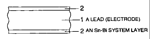
Fig. 1 shows a cross-sectional view of a lead
for a QFP-LSI according to the invention;
Fig. 2 shows a cross-sectional view of a lead
for a TSOP according to the invention;
Fig. 3 schematically shows a testing way of
evaluating solder-bonding strength;
Fig. 4 shows evaluation results of fillet
strength with regard to various types of metallized
leads according to the invention;
Fig. 5 shows evaluation results of wetting
CA 02493351 1998-12-09
7
time with regard to various types of metallized leads
according to the invention;
Fig. 6 shows evaluation results of wetting
force with regard to various types of metallized leads
according to the invention;
Fig. 7 shows evaluation results of fillet
strength in the case where there is formed a copper
layer according to the invention;
Fig. 8 shows evaluation results of flat
portion strength in the case where there is formed a
copper layer according to the invention;
Fig. 9 shows an observation result of an
interface region of a solder and a lead of an Fe-Ni
alloy (i.e. 42 alloy) on which an Sn-lOPb alloy plating
is provided according to the prior art, wherein (a) is
a cross-sectional view of the interface region, and (b)
are fractured surfaces at the lead side and the solder
side, respectively;
Fig. 10 shows an observation result of an
interface region of a solder and a lead of an Fe-Ni
alloy (i.e. 42 alloy) on which an Sn-4Bi alloy plating
is provided according to the invention, wherein (a) is
a cross-sectional view of the interface region, and (b)
are fractured surfaces at the lead side and the solder
side, respectively; and
Fig. 11 shows an observation result of an
interface region of a solder and a lead of an Fe-Ni
alloy (i.e. 42 alloy) of the invention on which an
CA 02493351 1998-12-09
8
under copper layer and an upper Sn-4Bi alloy plating is
provided according to the invention, wherein (a) is a
cross-sectional view of the interface region, and (b)
are fractured surfaces at the lead side and the solder
side, respectively.
REST MODE FOR CARRYING OUT THE INVENTION
Hereinafter, a description of embodiments
according to the invention will be provided.
One embodiment of the invention is an
electronic article, comprising a first and a second
electrodes both of which are bonded with each other by
means of a lead-free solder having low toxicity, the
first electrode being a QFP lead, a TSOP lead or the
like in an electronic device such as a semiconductor
device (e. g. LSI), for example, and the second
electrode being on a circuit board.
Another embodiment of the invention is a
bonded structure comprising a first and a second
electrodes both of which are bonded with each other by
means of a lead-free solder having low toxicity.
The lead-free solder having low toxicity can
be of an Sn-Ag-Hi alloy. With utilization of the Sn-
Ag-Bi alloy, it is required to obtain a bonding
interface which is stable with respect to a change in
process of time and has a bonding strength high enough
to withstand stress generated in solder-bonded portions
due to a difference in thermal expansion coefficient
between an electronic device and a circuit board, a
CA 02493351 1998-12-09
9
work of dividing the board after soldering, warping of
the board during the probing test, handling and so on.
It is also required to obtain an enough bonding
strength with utilization of the lead-free Sn-Ag-Bi
alloy solder by forming a sufficient fillet shape while
ensuring enough wettability at 220-240°C, which is a
suitable soldering temperature with respect to heat
resistance of circuit boards and electronic devices.
If the solder has inferior wettability, a sufficient
fillet shape can not be obtained resulting in that an
enough bonding strength is not obtained or a more
active flux is required leading to an adverse influence
on insulation resistance. Furthermore, it is also
necessary to ensure resistance to formation of
whiskers, etc. because short-circuit occurs between
electrodes if whiskers are generated and grow on the
electrode surface treated by plating, etc.
As shown in Figs. 1 and 2, an Sn-Hi layer 2
is formed on the surface of an electrode 1 of a lead to
obtain enough bonding strength as the electrode
structure of the invention. Next, a selection of an
electrode structure of the invention will be described.
Such selection was made by evaluating mainly bonding
strength, wettability and resistance to occurrence
whiskers based on the above requirements.
First, the result of an examination of the
bonding strength obtained between an Sn-Ag-Bi alloy
solder and various kinds of electrode materials are
CA 02493351 1998-12-09
1~
described. An outline of the experiment is illustrated
in Fig. 3. Sample leads 4 were formed by plating
lead-free materials of Sn, Sn-Bi, Sn-Zn and Sn-Ag
alloys, respective which are considered to be usable as
alternative materials for the the conventional Sn-10 Pb
alloy layer, onto leads each of which is an electrode
made of an Fe-Ni alloy (42 alloy). Besides, an
evaluation was also performed for combinations with the
conventional Sn-10 Pb alloy plating. The respective
example lead 4 was 3 mm wide and 38 mm long. It was
bent to form right angles so that the length of the
soldering section is 22 mm. The plating thickness was
approximately 10 pm for each composition. The
respective example lead 4 was soldered to a Cu pad (Cu
electrode) 7 on a glass epoxy substrate 6, which is a
circuit board, with utilization of a lead-free solder 5
of a 82.2 wt% Sn-2.8 wt% Ag-15 wt% Bi alloy
(hereinafter referred to as Sn-2.8Ag-lSBi).
The Cu pad (Cu electrode) 7 on the glass
epoxy substrate 6 had a size of 3.5 mm x 25 mm. The
solder 5 was provided in the form of a foil of 0.1 mm x
mm x 3.5 mm. More specifically, the solder foil 5
was placed on the Cu pad 7 on the glass epoxy substrate
6 and the example lead 4 being bent with the right
25 angle was placed on the solder foil 5. Soldering was
performed in the air at a maximum temperature of 220°C
after preheating at 140°C for 60 seconds. A rosin flux
containing chlorine was used when soldering. After
CA 02493351 1998-12-09
11
soldering, cleaning was conducted with an organic
solvent. The pull test was conducted in three cases;
i.e., a sample lead immediately after soldering,
another example lead exposed to a high temperature of
125°C for 168 hours after soldering taking account of
the deterioration of bonding strength due to a change
with the passage of time, and a further sample lead
after soldering following the exposure thereof to 150°C
for 168 hours to investigate bonding strength in the
case where wettability of lead is deteriorated. In the
pull test, the example lead was pulled vertically at a
rate of 5 mm/minute by gripping its distal end while
the substrate is fixed. Then a maximum strength and a
generally saturated constant strength were detected as
a fillet strength and a flat portion strength,
respectively, for the example lead of each composition.
The test was conducted ten times for each condition to
determine an average value.
The test results of the fillet strength of
the example lead of each composition are shown in Fig.
4. In plastic package devices such as ordinary
QFP-LSIs, it is necessary that fillet strength be at
least approximately 5 kgf in consideration of a
difference in thermal expansion coefficient of
printed-circuit board. From this, it became apparent
that an adequate bonding interface cannot be obtained
in the case of Sn-Zn, Sn-Ag and Sn-Pb alloy layers
although fillet strength of not less than 5 kgf was
CA 02493351 1998-12-09
12
obtained with the example leads in which an Sn layer or
Sn-Bi layers other than Sn-23Bi layers containing 23
wt% Bi are plated on the Fe-Ni alloy (42 alloy). In
addition to these example leads, further three types of
example leads were prepared by providing an Ni plating
layer having a thickness of about 2 pm onto the 42
alloy and plating the Ni layer with Au layer, a Pd
layer, and a Pd layer with a further Au layer,
respectively. Soldering was performed in the same
manner and bonding strength was investigated. However,
enough fillet strength was incapable of being obtained
as shown in Fig. 4. Accordingly, it became apparent
that it is necessary to apply an Sn-Bi layer to a lead
of an electrode.
Wettability to the Sn-2.8Ag-lSBi solder was
tested by the meniscograph method in the Sn-Bi alloy
plated leads which showed enough bonding strength in
the above pull test conducted on example leads of
various compositions. A flux of less activity was used
in order to investigate wettability. Test pieces were
obtained by cutting the above example leads into a
length of 1 cm. The wettability test was conducted
under the test conditions: a solder bath temperature of
220°C, an immersion speed of 1 mm/minute, an immersion
depth of 2 mm and an immersion time of 20 seconds. The
time which elapses till the load recovers to 0 (zero)
was regarded as wetting time and the load after
immersion for 20 seconds was regarded as wetting force.
CA 02493351 1998-12-09
13
Wettability was determined in two cases: a lead
immediately after plating and a lead exposed to 150°
for 168 hours after plating. Measurements were made
ten times for each test condition to obtain an average
value.
The wetting time and wetting force for each
composition are shown in Fig. 5 and Fig. 6,
respectively. It became apparent from the result of
wetting time shown in Fig. 5 that the higher the Bi
content, the better wettability in the Sn-Bi alloy
plated leads tested immediately after plating, while
wettability is deteriorated at below 1 wt% Bi and at 23
wt% Bi when the leads are exposed to a high temperature
of 150° for 168 hours. It can be said that at Bi
contents of below 1 wt%, wettability was low because
the wetting time became long while the wetting force
was ensured as shown in Fig. 6. Therefore, it became
apparent that a desirable Bi content is from 1 to 20
wt% in order to obtain sufficient wettability even with
the Sn-Bi alloy layer.
Stress generated in the interface is high
when materials with a great difference in thermal
expansion coefficient are bonded together, when
materials are used in an environment of great
temperature difference, and the like. The bonding
strength in the interface must be approximately 10 kgf
or more in order to ensure sufficient reliability.
Therefore, it became evident from Fig. 4 that fillet
CA 02493351 1998-12-09
14
strength of 10 kgf or more cannot be obtained by
directly providing an Sn-Bi layer onto the Fe-Ni alloy
(42 alloy). It is believed that this is because the
compounds at the interface are not sufficiently formed.
Therefore, a Cu plating layer of about 7 arm on average
was applied to the Fe-Ni alloy (42 alloy) and an Sn-Bi
alloy plating layer was applied to this Cu layer in
order to raise the reactivity with the solder in the
interface and bonding strength was measured. The
fillet strength, in the case of no Cu layer, is also
shown in Fig. 7. Bonding strength of not less than 10
kgf was obtained with the exception of the case of 23
wt% Bi and the effect of the underlayer of Cu was
capable of being verified. By adopting this electrode
structure it was possible to obtain a bonding strength
of about 12.1 kgf or more that is obtained immediately
after soldering of a lead made of the 42 alloy on which
an Sn-lOPb alloy layer is formed, which is soldered by
means of a eutectic Sn-Pb alloy solder, and whose
bonding strength is also shown as a comparative solder
in Fig. 7. Furthermore, as shown in Fig. 8, flat
portion strength was also capable of being improved by
forming a Cu layer under the Sn-Bi alloy layer. The Cu
layer may be applied to the 42 alloy as described above
when a lead frame of 42 alloy is used. However, when a
Cu lead frame is used, this lead frame may be allowed
to serve as the Cu layer or a further Cu layer may be
formed in order to eliminate the effect of other
CA 02493351 1998-12-09
elements which may sometimes be added to the lead frame
material to improve rigidity. The wettability of the
example leads to which this Cu layer is applied is also
shown in Figs. 5 and 6. There is scarcely any effect
5 of the Cu layer and sufficient wettability was capable
of being obtained at 1-20 wt% Bi, although wettability
also deteriorated at Bi contents of not more than 1 wt%
when the lead frames were exposed to a high
temperature. Incidentally, an Sn-2.8Ag-lSBi was used
10 in the examples shown in Figs. 7 and 8. However, the
formation of an underlayer of Cu is effective in
improving bonding strength even in systems of low Bi
content, for example, an Sn-2Ag-7.5,Bi-0.5Cu alloy.
The method of application of the above Sn-Bi
15 alloy and Cu layers is not limited to plating and these
layers can also be formed by dipping, deposition by
evaporation, roller coating or metal powder
application.
Thus, in order to investigate the reason why
various types of the electrode materials have different
strengths from one another, cross-sectional surfaces of
bonding portions were observed after polishing.
Further the fractured surfaces of samples subjected to
the pull test were observed under an SEM. The results
obtained in the typical combinations are described
below.
First, Fig. 9 shows an observation result in
the case where a lead obtained by applying an Sn-lOPb
CA 02493351 1998-12-09
16
alloy plating layer directly onto the conventional
Fe-Ni alloy (42 alloy) is bonded using an Sn-Ag-Bi
alloy solder. In this combination, Pb-Bi compounds
agglomerated at the interface and fracture occurred in
the interface between the 42 alloy and the solder. A
small amount of Sn was detected on the fractured 42
alloy surface of the lead and it is believed that the
Sn in the solder formed compounds with the 42 alloy of
lead. It is believed, therefore, that agglomaration of
the above compounds of Pb and Bi at the interface
reduced the contact area between Sn and 42 alloy,
greatly weakening bonding strength.
Next, Fig. 10 shows an observation result in
the case where the Sn-lOPb alloy plating layer was
replaced with an Sn-4Bi alloy plating layer. The
compound layer formed in the interface was thin and
fracture occurred similarly at the interface between 42
alloy and solder. However, Bi remained granular
crystals, which do not cause a decrease in the area of
bond between Sn and 42 alloy so much as in the case of
an Sn-lOPb. It is believed that this is the reason why
bonding strength of not less than 5 kgf was capable of
being obtained. Auger analysis revealed that the then
compound layer is an Sn-Fe layer of about 70 nm.
Fig. 11 shows an observation result in the
case where a Cu layer was formed on under the Sn-4Bi
layer. It was found that a thick layer of compounds of
Cu and Sn is formed in the interface. Fracture
CA 02493351 1998-12-09
17
occurred in the interface between this compound layer
and the solder or in the compound layer. The fractured
surface was almost flat in the case shown in Fig. 10
where the Sn-Bi alloy layer was directly formed on the
42 alloy lead, whereas it was uneven in the case where
the Cu layer was present. For this reason, it is
believed that this difference in the fractured surface
resulted in the improvement in bonding strength.
Incidentally, similar investigation results were
obtained also from other Sn-Ag-Bi alloy solder
compositions.
Occurrence of whiskers was investigated for
the above example leads of each composition. The
formation of whiskers was observed on the surfaces of
the example leads to which an Sn-Zn alloy plating layer
was applied. It has been hitherto said that Sn plating
presents a problem in resistance to the formation of
whiskers. However, the occurrence of whiskers was not
observed in the Sn-Bi alloy layers and there was no
problem in resistance to formation of whiskers.
Accordingly, with the use of the electrode
structures of the invention, the bonding portions
excellent in bonding strength, wettability and
resistance to occurrence of whiskers can be obtained by
means of Sn-Ag-Bi alloy solders.
The reason why Sn-Ag-Bi solders containing Sn
as a primary component, 5 to 25 wt% Bi, 1.5 to 3 wt% Ag
and optionally 0 to 1 wt% Cu were selected is that
CA 02493351 1998-12-09
18
solders of the composition in these ranges permit
soldering at 220-240°C and that these solders have
almost the same wettability as eutectic Sn-Ag alloy
solders, which have hitherto been field proven for Cu,
and provide sufficient reliability at high
temperatures. More specifically, Sn-Ag-Bi alloy
solders have a composition (a ternary eutectic alloy)
which melt at approximately 138°C when the Bi content
is not less than approximately 10 wt% and it is
concerned about that these portions might have an
adverse influence on reliability at high temperature.
However, the precipitation of a ternary eutectic
composition is controlled to levels that pose no
problem in practical use and high-temperature strength
at 125°C is also ensured. Accordingly; practical and
highly reliable electronic articles can be obtained by
soldering the above electrode using the solder of this
composition.
Example 1:
The cross-sectional structure of a lead for
QFP-LSI is shown in Fig. 1. This illustrates a part of
the cross-sectional structure of the lead. An Sn-Bi
alloy layer 2 was formed on a lead 1 which is of an
Fe-Ni alloy (42 alloy). The Sn-Bi alloy layer 2 was
formed by plating and its thickness was about 10 arm.
The Hi content of Sn-Bi alloy plating layer was 8 wt%.
The above QFP-LSI having this electrode structure was
CA 02493351 1998-12-09
19
soldered to a glass epoxy substrate, which is a circuit
board, with utilization of an Sn-2.8Ag-l5Bi-0.5Cu alloy
solder. Soldering was carried out in a reflow furnace
of a nitrogen environment at a peak temperature of
220°C. It was possible to obtain bonding portions
having sufficient bonding strength. Similarly, a
reflow soldering was carried out on a glass epoxy
substrate in the air at 240°C with utilization of an
Sn-2Ag-7.5Bi-0.5Cu alloy solder. Bonded portions
produced by reflow heating have high reliability
especially at a high temperature.
Example 2:
The cross-sectional structure of a TSOP lead
is shown in Fig. 2 which is a part of the lead
structure. A Cu layer 3 is formed on a lead 1 which is
of an Fe-Ni alloy (42 alloy) and an Sn-Bi alloy layer 2
is formed on this Cu layer. The Sn-Bi alloy layer 3
and Sn-Hi layer 2 were formed by plating. The
thickness of the Cu layer 3 was about 8 Nm and that of
the Sn-Bi plating layer was about 10 Nm. The Bi
content of Sn-Bi alloy plating layer was 5 wt%.
Because of high rigidity of the TSOP lead, when it is
used at a high temperature or under a condition that
heat generation occurs in the device itself, stress
generated at the interface is greater as compared with
the QFP-LSI. In such cases, it is necessary to form an
interface with sufficient bonding strength high enough
CA 02493351 1998-12-09
to withstand this interface stress and the Cu layer
under the Sn-Bi layer is effective for this purpose.
The TSOP was soldered to a printed-circuit
board in a vapor reflow furnace with utilization of an
5 Sn-Ag-Bi alloy solder and the thermal cycle test was
conducted. The test was conducted under the two test
conditions: one hour per cycle of -55°C for 30 minutes
and 125°C for 30 minutes,, and one hour per cycle of 0°C
for 30 minutes and 90°C for 30 minutes. After 500
10 cycles and 1,000 cycles the cross section was observed
and the condition of formation of cracks was
investigated. The cycle test result of crack
occurrence was compared with a case where a TSOP of the
same size having 42 alloy on which an Sn-lOPb alloy
15 layer is directly formed, was soldered using a eutectic
Sn-Pb alloy solder. Although cracks were formed early
in the thermal cycles of -55°C/125°C, no problems arose
with the thermal cycles of 0°C/90°C and a bonding
interface which is adequate for practical use was
20 obtained.
Example 3:
The electrode structures according to this
invention can also be applied in an electrode on a
board. For example, solder coating is effective in
improving the solderability of boards. Conventionally,
there have been used lead-containing solders such as a
eutectic Sn-Pb alloy solder. Thus, the Sn-Bi alloy
CA 02493351 1998-12-09
21
layer according to the invention can be used to make
the solder for coating lead-free. Furthermore, because
the electrode of a board is made of copper, sufficient
bonding strength can be obtained when an Sn-Ag-Bi alloy
solder is used. An example in which this structure is
applied is shown; an Sn-8Bi alloy layer of about 5 pm
was formed by roller coating on a Cu pad (Cu electrode)
on a glass epoxy substrate, which is a circuit board,
Wettability to boards and bonding strength
were improved, because the solder layer was formed.
INDUSTRIAL APPLICABILITY
An electrode structure can be realized, which
is suitable for an Sn-Ag-Bi alloy solder excellent as a
lead-free material.
A bonded structure by a lead-free solder can
be realized with utilization of a lead-free Sn-Ag-Bi
alloy solder, in which an bonding interface which is
stable and has sufficient bonding strength can be
obtained.
An electronic article can be realized with
utilization of a lead-free Sn-Ag-Bi alloy solder of low
toxicity, which has a bonded structure by the lead-free
solder, which can provide a stable bonding interface
with respect to a change in process of time and a
strength high enough to withstand stress generated in
bonded portions by soldering due to a difference in
thermal expansion coefficient between electric devices
CA 02493351 1998-12-09
22
and a board, a work of dividing the board after
soldering, warping of the board during the probing
test, handling and so on.
With utilization of a lead-free Sn-Ag-Bi
alloy solder of low toxicity, it is possible to obtain
sufficient bonding strength by forming adequate fillets
while ensuring sufficient wettability, for example, at
220-240° and to ensure resistance to formation of
whiskers, etc.
Soldering electronic devices with utilization
of an Sn-Ag-Bi solder makes it possible to obtain an
interface which has sufficient bonding strength and to
ensure wettability which is sufficient for practical
use. There is no problem in resistance to formation of
whiskers. Thus it is possible to realize lead-free
electrical appliances which are environmentally
friendly by using the same equipment and process as
conventionally.