Note: Descriptions are shown in the official language in which they were submitted.
CA 02495486 2011-04-28
APPARATUS AND METHOD FOR CHARGING AND DISCHARGING
A CAPACITOR TO A PREDETERIVIENED SETPOINT
FIELD OF THE INVENTION
[0002] The present invention relates to electronic methods and
circuits for
controlling proportional general purpose smart material based actuators.
BACKGROUND OF THE INVENTION
[0003] Actuator technologies are being developed for a wide range
of
applications. One example includes a mechanically leveraged smart material
actuator
that changes shape in response to electrical stimulus. This change in shape is
proportional to the input voltage. Since this shape change can be effectuated
predominantly along a single axis, such actuators can be used to perform work
on
associated mechanical systems including a lever in combination with some main
support structure. Changes in axial displacement are magnified by the lever to
create
an actuator with a useful amount of force and displacement. Such force and
displacement is useful for general-purpose industrial valves, clamps, beverage
dispensers, compressors or pumps, brakes, door locks, electric relays, circuit
breakers, and other applications actuated by means including solenoids, motors
or
motors combined with various transmission means. Smart materials, however, and
piezoelectric materials specifically, can require hundreds of volts to actuate
and cause
displacement. This type of voltage may not be readily available and may have
to be
derived from a lower voltage as one would find with a battery.
[0004] Another characteristic of piezoelectric materials is that the
materials are
capacitive in nature. Moreover, a single actuator is often controlled using
three
separate signals: a control signal, a main supply and a ground.
CA 02495486 2011-04-28
2
SUMMARY OF THE INVENTION
[0005] Accordingly, in one aspect there is provided an apparatus for
charging and
discharging a capacitor to predetermined setpoints comprising, a smart
material
actuator, a voltage controlled DC to DC converter for operating the smart
material
actuator in a proportional manner, a constant supply voltage to supply the
voltage
controlled DC to DC converter, and a control signal providing a selectable
input
voltage, wherein an output voltage of the DC to DC converter is applied to the
smart
material actuator and wherein the output voltage is proportional to the
selectable
input voltage.
[0005a] The voltage controlled DC to DC converter can further include a
self-
oscillating drive circuit connected to a primary coil of a transformer with
push-pull
drive signals 180 degrees out of phase. The voltage controlled DC to DC
converter
can also include an auxiliary coil on the transformer. An attached diode
rectifier to
generate a DC voltage from an AC signal of the secondary coil on the
transformer
can also be included with the DC to DC converter as well as a voltage feedback
network for voltage regulation.
[0006] The voltage controlled DC to DC converter can further include
control
circuitry for stopping and starting the self-oscillating mechanism and can
also feature
a diode on an input stage for reverse polarity protection. Moreover, the
control
circuitry can further include a bead inductor and bypass capacitor for
suppression of
radiated EMI into the power source of the system.
[0007] Another feature of the invention includes a smart material drive
circuit for
actively charging and discharging the smart material actuator in response to
connecting and disconnecting a power source respectively. The drive circuit
for
actively controlling at least one of charging and discharging the smart
material
actuator can be responsive to a control signal.
[0008] According to another aspect there is provided an apparatus for
charging and
discharging a capacitor to predetermined setpoints comprising a smart material
actuator, a power source connectible to the smart material actuator, and a
switch
circuit for actively discharging the smart material actuator in response to
removal of
the connection to the power source. The switch circuit for actively charging
the
CA 02495486 2011-04-28
3
smart material actuator can further be responsive to connecting the power
source or a
control signal input. The switch circuit can actively control at least one of
charging
and discharging the smart material actuator in response to a control signal
and can
further include a voltage comparator and field effect transistor (FET) to
control the
DC to DC converter. The switch can, according to the invention, have three
operational modes, charge load, hold load and discharge load.
[0008a] According to yet another aspect there is provided a method for
charging and
discharging a capacitor to predetermined setpoints comprising the steps of
providing
a smart material actuator, operating the smart material actuator in a
proportional
manner with a voltage controlled DC to DC converter, supplying a constant
supply
voltage to the voltage controlled DC to DC converter, and providing a control
signal
having a selectable input voltage wherein an output voltage of the DC to DC
converter is applied to the smart material actuator and wherein the output
voltage is
proportional to the selectable input voltage.
[0008b] According to still yet another aspect there is provided a method
for charging
and discharging a capacitor to predetermined setpoints comprising the steps of
providing a smart material actuator, connecting a power source to the smart
material
actuator, and actively discharging the smart material actuator in response to
removal
of the connection to the power source with a switch circuit.
[0009] With the use of electronic design and simulation software and
electronic
prototyping of the circuit, details for using a minimum number of components
while
maintaining a cost-effective, and low power solution are realized. This
electronic
subsystem, when coupled to a mechanically leveraged smart material actuator,
creates a commercially viable proportional actuator solution for general
purposes and
industrial applications.
CA 02495486 2011-04-28
3a
[0010] Other applications of the present invention will become apparent
to those
skilled in the art when the following description of the best mode
contemplated
for practicing the invention is read in conjunction with the accompanying
drawings.
BRIEF DESCRIPTION OF THE DRAWINGS
[0011] The description herein makes reference to the accompanying
drawings
wherein like reference numerals refer to like parts throughout the several
views, and
wherein:
[0012] Fig. 1 is an electronic schematic of a voltage controlled DC to DC
converter
with active regulation to which the present invention is applied;
[0013] Fig. 2 is an electronic schematic of a DC to DC converter of the
present
invention;
[0014] Fig. 3 is an electronic schematic of the electronic switch of the
present
invention illustrating current flow when the switch is closed;
[0015] Fig. 4 is an electronic schematic of the electronic switch of the
present
invention illustrating current flow when the switch is open; and
CA 02495486 2005-02-04
WO 2004/023636 PCT/US2003/023751
4
[0016] Fig. 5 is an electronic schematic of the control circuit of
the present
invention.
DESCRIPTION OF THE PREFERRED EMBODIMENT
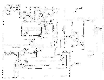
[0017] Figure 1 shows an electronic schematic of a system 10 for
controlling a
proportional mechanically leveraged smart material actuator (not shown)
including a
specialized power source 12 coupled to switching circuitry 44 and control
circuitry
64.
[0018] According to the preferred embodiment, the specialized power
source
of Figure 1 is a DC to DC converter, switching circuit, and control circuit
operative either to supply a variable stimulating voltage or to actively
discharge the
actuator. As best shown in Figure 2, the DC to DC converter 12 (12 is missing
from
Fig 2.) includes a supply voltage 14 connected to a bead inductor 16 which
feeds
reverse protection diode 18. Bead inductor 16 acts as a filter to remove noise
generated by the collector of negative positive negative (NPN) transistor 20
connected to the supply voltage 14. NPN transistor 20 and NPN transistor 22
form a
push-pull driver for transformer 24. Resistors 26, 28, 30, and 32 form a
resistive
voltage divider and set the basic bias points for NPN transistors 20 and 22.
[0019] Transformer 24 is wound not only with a primary coil 24a and
a
secondary coil 24b, but an auxiliary coil 24c. Auxiliary winding 24c,
transformer 24,
resistors 34, 36, 28, and capacitors 38, 40 form feedback means to cause
oscillation
on the base of NPN transistors 20, 22. Oscillation is 180 degrees out of phase
between the two NPN transistors 20, 22 forming a self-oscillating push-pull
transformer driver. The secondary coil 24b of transformer 24 is connected to
rectifier
42. It should be noted that when the base of transistor 22 is grounded, the
self-
oscillating mechanism is stopped. When the ground is removed, the self-
oscillating
mechanism is restarted. As shown in Figure 1, switch circuitry 44, when
commanded, is capable of actively controlling the voltage to the capacitive
load.
[0020] Control circuitry 64 monitors the control voltage and output
voltage
and makes the decision to turn on the DC to DC converter, or turn on the
discharge
switch, or hold the current voltage level at the capacitive load. Included in
the
CA 02495486 2005-02-04
WO 2004/023636 PCT/US2003/023751
system is means for forcing the capacitive load to ground should the supply
voltage
be removed.
[0021] Referring now to Figure 3, switching circuitry 44 is
depicted isolated
from the schematic of Figure 1 to better illustrate the operative features of
the
switching circuitry 44 when it is closed. When switch 48 is closed, current
flows
from a power source 50 through switch 48 through bead inductor 52 charging the
capacitive load 54. Also, current flows into resistive divider network 56
driving the
NPN transistor 58 on, which turns NPN Darlington pair 60 off. The rate of
charge is
determined by the impedance of the power source and the capacitance of the
load 54.
Resistor 62 and NPN transistor 58 serve as a level translator between the
switched
power and control signal, so the switched power and control signal do not have
to
have the same voltage levels.
[0022] Referring now to Figure 4, the current flow in switching
circuitry 44 is
shown when switch 48 is open. When switch 48 is open, no current flows from
the
power source 50. Also, current flows into resistive divider network 56 through
switch 48 to ground, driving the NPN transistor 58 off, which turns NPN
Darlington
pair 60 on causing current flow through resistor 46 discharging capacitive
load 54.
The rate of discharge is determined by the value of resistor 46 and capacitive
load 54.
Resistor 62 and NPN transistor 58 serve as a level translator between the
switched
power and control signal so the switched power and control signal do not have
to
have the same voltage levels.
[0023] Referring now to Figure 5, the control circuit 64 of Figure
1 is shown
isolated to better illustrate the operative features of the circuit 64. Analog
control
voltage flows through resistor 66 and is clamped by Zener diode 68 at a preset
voltage so as not to damage the input of operational amplifier 70. Further,
resistor 66
is part of resistive dividing network 72. The network 72 derives two voltages;
one
voltage is the reference to shut the DC to DC converter 12 down, the other, a
reference to actively discharge the capacitive load. Operational amplifier 70
is used
in a voltage comparator mode that is associated with the DC to DC converter 12
shutdown mode. Operational amplifier 74 is used in a voltage comparator mode
and
is associated with the active discharge mode. Resistors 76, 78, 80 form a
second
CA 02495486 2005-02-04
WO 2004/023636 PCT/US2003/023751
6
resistive voltage divider network. This network monitors the capacitive load
voltage
and derives the voltages that operational amplifiers 70, 74 compare to the
reference
voltages derived from resistors 66, 72. When the voltage at the plus terminal
of
operational amplifier 70 is greater than the minus, the output of the
amplifier goes to
the plus saturation state turning FET transistor 82 on causing the DC to DC
converter
to stop.
[0024] When the voltage at the minus terminal of operational
amplifier 70 is
greater than the plus, the output of the amplifier goes to the minus
saturation state
turning FET transistor 82 off causing the DC to DC converter to run. When the
voltage at the plus terminal of operational amplifier 74 is greater than the
minus the
output of the amplifier goes to the plus saturation state turning FET
transistor 84 on
causing the active discharge of capacitive load. When the voltage at the minus
terminal of operational amplifier 74 is greater than the plus, the output of
the
amplifier goes to the minus saturation state turning FET transistor 84 off. In
this
system there are three distinct states, (1) DC to DC converter on and
capacitive load
discharge switch open, (2) DC to DC converter off and capacitive load
discharge
switch open, and (3) DC to DC converter off and capacitive load discharge
switch on.
[0025] In the embodiment illustrated in Figures 1, 2, 3, 4, and 5,
the
components have been chosen for their current carrying ability, voltage
rating, and
type. Other suitable components can include FET small signal, and power
transistors, wire wound, thin film, and carbon comp resistors, ceramic,
tantalum, and
film capacitors, wound, and Low Temperature cofired ceramic (LTCC)
transformers,
or any combination of suitable components commonly used for high volume
production. Although these materials given as examples provide excellent
performance, depending on the requirements of an application, use of other
combinations of components can be appropriate. Likewise, the embodiment
illustrates components that are commercially available.
[0026] While the invention has been described in conjunction with
what is
presently considered to be the most practical and preferred embodiment, it is
to be
understood that the invention is not to be limited to the disclosed embodiment
but, on
the contrary, it is intended to cover various modifications and equivalent
CA 02495486 2005-02-04
WO 2004/023636
PCT/US2003/023751
7
arrangements included within the spirit and scope of the appended claims,
which
scope is to be accorded the broadest interpretation so as to encompass all
such
modifications and equivalent structures as permitted under law.