Language selection

Search

Patent 2496296 Summary

Third-party information liability

Some of the information on this Web page has been provided by external sources. The Government of Canada is not responsible for the accuracy, reliability or currency of the information supplied by external sources. Users wishing to rely upon this information should consult directly with the source of the information. Content provided by external sources is not subject to official languages, privacy and accessibility requirements.

Claims and Abstract availability

Any discrepancies in the text and image of the Claims and Abstract are due to differing posting times. Text of the Claims and Abstract are posted:

  • At the time the application is open to public inspection;
  • At the time of issue of the patent (grant).
(12) Patent Application: (11) CA 2496296
(54) English Title: DIFFRACTION GRATING-BASED ENCODED MICRO-PARTICLES FOR MULTIPLEXED EXPERIMENTS
(54) French Title: MICROPARTICULES CODEES BASEES SUR UN RESEAU DE DIFFRACTION POUR EXPERIENCES MULTIPLEXEES
Status: Dead
Bibliographic Data
(51) International Patent Classification (IPC):
  • G06K 19/06 (2006.01)
  • C40B 70/00 (2006.01)
  • G06K 7/10 (2006.01)
  • C12Q 1/68 (2006.01)
  • C40B 30/04 (2006.01)
  • G02B 5/18 (2006.01)
(72) Inventors :
  • MOON, JOHN (United States of America)
  • PUTNAM, MARTIN A. (United States of America)
(73) Owners :
  • CYVERA CORPORATION (United States of America)
(71) Applicants :
  • CYVERA CORPORATION (United States of America)
(74) Agent: GOWLING LAFLEUR HENDERSON LLP
(74) Associate agent:
(45) Issued:
(86) PCT Filing Date: 2003-08-20
(87) Open to Public Inspection: 2004-03-04
Examination requested: 2008-08-19
Availability of licence: N/A
(25) Language of filing: English

Patent Cooperation Treaty (PCT): Yes
(86) PCT Filing Number: PCT/US2003/026316
(87) International Publication Number: WO2004/019277
(85) National Entry: 2005-02-18

(30) Application Priority Data:
Application No. Country/Territory Date
60/405,087 United States of America 2002-08-20
60/410,541 United States of America 2002-09-12

Abstracts

English Abstract


Microparticles (8) includes an optical substrate (10) having at least one
diffraction grating (12) disposed therein. The grating (12) having a plurality
of colocated pitches .LAMBDA. which represent a unique identification digital
code that is detected when illuminated by incident light (24). The incident
light (24) may be directed transversely from the side of the substrate (10)
with a narrow band (single wavelength) or multiple wavelength source, in which
case the code is represented by a spatial distribution of light or a
wavelength spectrum, respectively. The code may be digital binary or may be
other numerical bases. The micro-particles (8) can provide a large number of
unique codes, e.g., greater than 67 million codes, and can withstand harsh
environments. The micro~particles (8) are functionalized by coating them with
a material/substance of interest, which are then used to perform multiplexed
experiments involving chemical processes, e.g., DNA testing and combinatorial
chemistry.


French Abstract

Un système de microparticules (8) comprend un substrat optique (10) possédant au moins un réseau de diffraction (12). Le réseau (12) possédant une pluralité de points co-implantés ?, qui représentent un code numérique d'identification unique, est détecté lorsqu'on l'éclaire avec une lumière incidente (24). La lumière incidente (24) peut être dirigée transversalement à partir du côté du substrat (10) avec une source à bande étroite (longueur d'onde unique) ou à longueurs d'ondes multiples, et dans ce dernier cas le code est représenté par une répartition spatiale de la lumière ou d'un spectre de longueurs d'onde, respectivement. Le code peut être numérique binaire ou avoir d'autres bases numériques. Le système de microparticules (8) permet de former un grand nombre de codes uniques, p. ex. plus de 67 millions de codes, et résiste aux environnements hostiles. Les microparticules (8) sont fonctionnalisées par un revêtement fait d'un matériau / d'une substance d'intérêt, qui sont ensuite utilisés pour conduire des expériences multiplexées impliquant des processus chimiques, p. ex., des tests d'ADN ou des réactions chimiques combinatoires.

Claims

Note: Claims are shown in the official language in which they were submitted.


CLAIMS

What is claimed is:

1. An optical identification element having a chemical attached thereto,
comprising:
a substrate
at least a portion of said substrate having at least one diffraction grating
disposed
therein, said grating having at least one refractive index variation pitch
superimposed at a
grating location;
the grating providing an output optical signal indicative of a code when
illuminated by an incident light signal propagating in free space; and
the chemical being attached to at least a portion of said substrate.

2. The apparatus of claim 1 wherein said grating comprises a plurality of
refractive index pitches superimposed at said grating location, the
combination of said
pitches providing a resultant refractive index variation.

3. The apparatus of claim 1 wherein said substrate is made of a material
selected from the group: glass, plastic, rubber, and polymer.

4. The apparatus of claim 1 wherein said substrate comprises a glass
material.

5. The apparatus of claim 1 wherein said substrate comprises silica.

6. The apparatus of claim 1 wherein said grating comprises a plurality of
refractive index pitches superimposed at said grating location.

7. The apparatus of claim 1 wherein said code comprises a plurality of digital
bits.

8. The apparatus of claim 1 wherein said code comprises at least a
predetermined number of bits, said number being: 3, 5, 7, 9, 10, 12, 14, 16,
18, 20, 24,
28, 30, 40, 50, or 100.

9. The apparatus of claim 1 wherein said code comprises a plurality of bits,
each bit having a plurality of states.

10. The apparatus of claim 1 wherein said code comprises a plurality of bits,
each bit having a corresponding spatial location and each bit in said code
having a value
related to the intensity of said output optical signal at the spatial location
of each bit.

17


11. The apparatus of claim 10 wherein the value of each bit corresponds to the
magnitude of refractive index variation of a corresponding refractive index
pitch in said
grating.
12. The apparatus of claim 1 wherein said code comprises a plurality of
digital
bits, each bit having a corresponding spatial location and each bit in said
code having a
binary value related to the intensity of said output optical signal at the
spatial location of
each bit.
13. The apparatus of claim 12 wherein the value of each bit corresponds to the
presence or absence of a corresponding refractive index pitch in said grating.
14. The apparatus of claim 1 wherein said incident light comprises a single
wavelength.
15. The apparatus of claim 1 wherein said incident light comprises a plurality
of wavelengths or a single wavelength scanned over a predetermined wavelength
range.
16. The apparatus of claim 15 wherein said code comprises a plurality of bits,
and each bit in said code having a value related to the intensity of said
output optical
signal at a wavelength corresponding to each bit.
17. The apparatus of claim 16 wherein the value of each bit corresponds to the
magnitude of refractive index variation of a corresponding refractive index
pitch in said
grating.
18. The apparatus of claim 15 wherein said code comprises a plurality of
digital bits, and each bit in said code having a binary value related to the
intensity of said
output optical signal at the wavelength corresponding to each bit.
19. The apparatus of claim 18 wherein the value of each bit corresponds to the
presence or absence of corresponding refractive index pitch in said grating.
20. The apparatus of claim 1 wherein, said substrate has a length that is less
than about 500 microns.
21. The apparatus of claim 1 wherein said substrate has a diameter that is
less
than about 125 microns.
22. The apparatus of claim 1, wherein said substrate has a reflective coating
disposed thereon.


18


23. The apparatus of claim 1 wherein, said substrate has a coating disposed on
at least a portion of said substrate, at least a portion of said coating being
made of a
material that allows sufficient amount of said incident light signal to pass
through said
material to allow detection of said coda.
24. The apparatus of claim 1 wherein said substrate has a coating material
disposed on at least a portion of said substrate, said coating comprising a
polymer.
25. The apparatus of claim 1 wherein said substrate has a magnetic or electric
charge polarization.
26. The apparatus of claim 1 wherein said substrate has a cylindrical shape.
27. The apparatus of claim 1 wherein said substrate has geometry having
holes therein.
28. The apparatus of claim 1 wherein said substrate has a geometry having
protruding sections.
29. The apparatus of claim 1 wherein at least a portion of said substrate has
an
end cross sectional geometry selected from the group: circular, square,
rectangular.
elliptical, clam-shell, D-shaped, and polygon.
30. The apparatus of claim 1 wherein at least a portion of said substrate has
a
side view geometry selected from the group: circular, square, rectangular,
elliptical,
clam-shell, D-shaped, and polygon.
31. The apparatus of claim 1 wherein at least a portion of said substrate has
a
3-D shape selected from the group: sphere, a cube, and a pyramid.
32. The apparatus of claim 1, wherein said substrate has a grating region
where
said grating is located anal a non-grating region where said grating is not
located; and
wherein said substrate has a plurality of grating regions.
33. The apparatus of claim 1 wherein said substrate has a grating region where
said grating is located and a non-grating region where said grating is not
located; and
wherein sand grating region has a refractive index that is greater than that
of said non-
grating rebion.
34. The apparatus of claim 1. wherein said substrate has a grating region
where
said grating is located and a non-grating region where said grating is not
located; and


wherein said grating region has a refractive index that is not greater than
that of said non-
grating region.

35. The apparatus of claim 1 wherein said incident light is incident on said
substrate along a longitudinal grating axis of said grating.

36. The apparatus of claim 1 wherein said incident light is incident on said
substrate at an angle to a longitudinal grating axis of said grating.

37. The method of claim 1 wherein said incident light comprises laser light.

38. The apparatus of claim 1 wherein said grating is a blazed grating.

39. The apparatus of claim 1 wherein said grating comprises a thin grating.

40. The apparatus of claim 1 wherein said substrate comprises a plurality of
said gratings.

41. The apparatus of claim 1 wherein said substrate comprises a plurality of
said gratings each at different locations within said substrate.

42. The apparatus of claim 1 wherein said substrate comprises a particle or
bead.

43. The apparatus of claim 1 wherein said chemical comprises at least one
gene, oligonucleotide, protein, antibody, peptide, amino acid, NDA, cDNA, RNA,
nucleic acid oligomer, polymer, or biological cell, or portion thereof.

44. An encoded particle having a chemical attached thereto, comprising:
a particle, at least a portion of which having at least one diffraction
grating
disposed therein, said grating having a resultant refractive index variation
at a grating
location;
said grating providing an output optical signal indicative of a code when
illuminated by an incident light signal; and
the chemical being attached to at least a portion of said particle.

45. The apparatus of claim 44 wherein said grating comprises at least one
refractive index pitch superimposed at said grating location, the combination
of said at
least one pitch providing said resultant refractive index variation.

46. The apparatus of claim 44 wherein said grating comprises a plurality of
refractive index pitches superimposed at said grating location, the
combination of said
pitches providing said resultant refractive index variation.

21


47. The apparatus of claim 44 wherein said particle is made of a material
selected from the group: glass, plastic, rubber, and polymer.
48. The apparatus of claim. 44 wherein sand particle comprises a glass
material.
49. The apparatus of claim 44 wherein said particle comprises silica.
50. The apparatus of claim 44 wherein said grating comprises a plurality of'
refractive index pitches superimposed at said grating location.
51. The apparatus of claim 44 wherein said code comprises a plurality of
digital bits.
52. The apparatus of claim 44 wherein said code comprises at least a
predetermined number of bits, said number being; 3, 5, 7, 9, 10, 12, 14, 16,
18, 20, 24,
28, 30, 40, 50, or 100.
53. The apparatus of claim 44 wherein, said code comprises a plurality of
bits,
each bit having a plurality of states,
54. The apparatus of claim 44 wherein, said code comprises a plurality of bits
each bit having a corresponding spatial location and each bit in said code
having a value
related to the intensity of said output optical signal at the spatial location
of each bit.
55. The apparatus of claim 54 wherein the value of each bit corresponds to the
magnitude of refractive index variation of a corresponding refractive index
pitch in said
grating.
56. The apparatus of claim 44 wherein said code comprises a plurality of
digital bits, each bit having a corresponding spatial location and each bit in
said code
having a binary value related to the intensity of said output optical signal
at the spatial
location of each bit.
57. The apparatus of claim, 56 wherein the value of each bit corresponds to
the
presence or absence of a corresponding refractive index pitch, in a said
grating.
58. The apparatus of claim 44 wherein said incident light comprises a single
wavelength.
59. The apparatus of claim 44 wherein said incident light comprises a
plurality of wavelengths or a single wavelength scanned over a predetermined
wavelength range.
22


60. The apparatus of claim 59 wherein said code comprises a plurality of bits,
and each bit in said code having a value related to the intensity of said
output optical
signal at a wavelength corresponding to each bit.
61. The apparatus of claim 60 wherein the value of each bit corresponds to the
magnitude of refractive index variation of a corresponding refractive index
pitch in said
grating.
62. The apparatus of claim 59 wherein, said code comprises a plurality of
digital bits, and each bit in said code having a binary value related to the
intensity of said
output optical signal at the wavelength corresponding to each bit.
63. The apparatus of claim 62 wherein the value of each bit corresponds to the
presence or absence of a corresponding refractive index pitch in said grating.
64. The apparatus of claim 44 wherein said particle has a length that is less
than about 500 microns.
66. The apparatus of claim 44 wherein said particle has a diameter that is
less
than about 125 microns.
66. The apparatus of claim 44 wherein, said particle has a reflective coating
disposed thereon.
67. The apparatus of claim 44 wherein said particle has a coating disposed on
at least a portion of said particle, at least a portion of said coating being
made of a
material that allows sufficient amount of said incident light signal, to pass
through said
material to allow detection of said code.
68. The apparatus of claim 44 wherein said particle has a coating material
disposed on at least a portion of said particle, said coating comprising a
polymer.
69. The apparatus of claim, 44 wherein said particle has a magnetic or
electric
charge polarization.
70. The apparatus of claim 44 wherein said particle has a cylindrical shape.
71. The apparatus of claim 44 wherein said particle has geometry having holes
therein.
72. The apparatus of claim 44 wherein said particle has a geometry having
protruding sections.

23


73. The apparatus of claim 44 wherein at least a portion of said particle has
an
end cross sectional geometry selected from the group: circular, square,
rectangular,
elliptical, clam-shell, D-shaped, and polygon.
74. The apparatus of claim 44 wherein at least a portion of said particle has
a
side view geometry selected from, the group: circular, square, rectangular
elliptical,
clam-shell, D-shaped, and. polygon.
75. The apparatus of claim 44 wherein at least a portion of said particle has
a
3-D shape selected from the group: sphere, a cube, and a pyramid,
76. The apparatus of claim 44 wherein said particle has a grating region where
said dating is located and a non-grating region where said grating is not
located; and
wherein said particle has a plurality of grating regions.
77. The apparatus of claim 44 wherein said particle has a grating region where
said grating is located and a non-grating region where said grating is not
located and
wherein said grating region has a refractive index that is greater than that
of said non-
grating region.
78. The apparatus of claim 44 wherein said particle has a grating region where
said grating is located anal a non-grating region where said grating is not
located and
wherein said grating region, has a refractive index that is not greater than
that of said non-
grating region.
79. The apparatus of claim 44 wherein said incident light is incident on said
particle along a longitudinal grating axis of said grating.
80. The apparatus of, claim 44 wherein said incident light is incident on said
particle at an angle to a longitudinal grating axis of said grating.
81. The method of claim 44 wherein said incident light comprises laser light.
82. The apparatus of claim 44 wherein said grating is a blazed grating.
83. The apparatus of claim 44 wherein said grating comprises a thin grating.
84. The apparatus of claim 44 wherein said particle comprises a plurality of
said gratings.
85. The apparatus of claim 44 wherein said particle comprises a plurality of
said gratings each at different locations within said particle.


24


86. The apparatus of claim 44 wherein said chemical comprises at last one
gene, oligonucleotide, protein, antibody, peptide, amino acid, NDA, cDNA, RNA,
nucleic acid oligomer, polymer, or biological cell, or portion thereof.
87. A method of reading an encoded optical identification element having a
chemical attached thereto, comprising:
obtaining a substrate, at least a portion of which having at least one
diffraction
grating disposed therein, said grating having at least one refractive index
variation pitch
disposed at a grating location;
attaching the chemical to at least a portion of said substrate;
illuminating said substrate with incident light propagating in free space,
said
substrate providing an output light signal indicative of a code; and
reading said output light signal and detecting said code therefrom.
88. The method of claim 87 wherein said grating comprises a plurality of
refractive index pitches superimposed at said grating location, the
combination of said
pitches providing a resultant refractive index variation.
89. The method of claim 87 wherein said substrate is made of a material.
selected from the group: glass, plastic, rubber and polymer.
90. The method of claim 87 wherein said substrate comprises a glass material.
91. The method of claim 87 wherein said substrate comprises silica.
92. The method of claim 87 wherein said grating comprises a plurality of
refractive index pitches superimposed at said grating location.
93. The method of claim 87 wherein said code comprises a plurality of digital
bits.
94. The method of claim 87 wherein said code comprises at least a
predetermined number of bits, said number being: 3, 5, 7, 9, 10,11, 14, 16,
18, 20, 24,
28, 30, 40, 50, or 100.
95. The method of claim 87 wherein said code comprises a plurality of bits,
each bit having a plurality of states.
96. The method of claim 87 wherein said code comprises a plurality of bits,
each bit having a corresponding spatial location and each bit in said code
having a value
related to the intensity of said output optical signal at the spatial location
of each bit.


25


97. The method of claim 96 wherein the value of each bit corresponds to the
magnitude of refractive index variation of a corresponding refractive index
pitch in said
grating.
98. The method of claim 87 wherein said code comprises a plurality of digital
bits, each bit having a corresponding spatial location and each bit in said
code having a
binary value related to the intensity of said output optical signal at the
spatial location of
each bit.
99. The method of claim 98 wherein the value of each bit corresponds to the
presence or absence of a corresponding refractive index pitch in said grating.
100. The method of claim 87 wherein said incident light comprises a single
wavelength.
101. The method of claim 87 wherein said substrate has a coating disposed on
at least a portion of said substrate, at least a portion of said coating being
made of a
material that allows sufficient amount of said incident light signal to pass
through said
material to allow detection of said code,
102. The method of claim 87 wherein said substrate has a coating material
disposed on at least a portion of said substrate, said coating comprising a
polymer.
103. The method of claim 87 wherein at least a portion of said substrate has a
3-D shape selected from the group; a cylinder, a sphere, a cube, and a
pyramid.
104. The method of claim 87 wherein said substrate has a grating region where
said grating is located and a non-grating region where said grating is not
located; and
wherein said substrate has a plurality of grating regions.
105. The method of claim 87 wherein said substrate loan a grating region where
said grating is located and a non-grating region where said grating is not
located and
wherein said grating region has a refractive index that is greater than that
of said non-
grating region.
106. The method of claim 87 wherein said substrate has a grating region where
said grating is located and a non-grating region where said grating is not
located; and
wherein said grating region has a refractive index that is not greater than
that of said non-
grating region.

26


107. The method of claim 87 wherein said incident light is incident on said
substrate along a longitudinal grating axis of said grating.

108. The method of claim 87 wherein said incident light is incident on said
substrate at an angle to a longitudinal grating axis of said grating.

109. The method of claim 87 wherein said grating comprises a thin grating.

110. The method of claim 87 wherein said substrate comprises a plurality of
said gratings.

111. The method of claim 87 wherein said substrate comprises a plurality of
said gratings each at different locations within said substrate.

112. The method of claim 87 wherein said substrate comprises a particle or
bead.

113. The method of claim 87 wherein said chemical comprises at least one
gene, oligonucleotide, protein, antibody, peptide, amino acid, NDA, cDNA, RNA,
nucleic acid oligomer, polymer, or biological cell, or portion thereof.

114. A method of reading an encoded particle having a chemical attached
thereto, comprising:
obtaining a particle, at least a portion of which having at least one
diffraction
grating disposed therein, said grating having a resultant refractive index
variation at a
grating location;
attaching the chemical to at least a portion of said particle;
illuminating said particle with incident light, said particle providing an
output
light signal indicative of a code; and
reading said output light signal and detecting said code therefrom.

115. The method of claim 114 wherein said grating comprises at least one
refractive index pitch superimposed at said grating location, the combination
of said at
least one pitch providing said resultant refractive index variation.

116. The method of claim 114 wherein said grating comprises a plurality of
refractive index pitches superimposed at said grating location, the
combination of said
pitches providing said resultant refractive index variation.

117. The method of claim 114 wherein said particle is made of a material
selected from the group: glass, plastic, rubber, and polymer.

27


118. The method of claim 114 wherein said particle comprises a glass material.

119. The method of claim 114 wherein said particle comprises silica.

120. The method of claim 114 wherein said particle comprises a plurality of
refractive index pitches superimposed at said grating location.

121. The method of claim 114 wherein said particle comprises a plurality of
digital bits.

122. The method of claim 114 wherein said particle comprises at least a
predetermined number of bits, said number being: 3, 5, 7, 9, 10, 12, 14, 16,
18, 20, 24,
28, 30, 40, 50, or 100.

123. The method of claim 114 wherein said code comprises a plurality of bits,
each bit having a plurality of states.

124. The method of claim 114 wherein said code comprises a plurality of bits,
each bit having a corresponding spatial location and each bit in said code
having a value
related to the intensity of said output optical signal at the spatial location
of each bit.

125. The method of claim 124 wherein the value of each bit corresponds to the
magnitude of refractive index variation of a corresponding refractive index
pitch in said
grating.

126. The method of claim 114 wherein said code comprises a plurality of
digital bits, each bit having a corresponding spatial location and each bit in
said code
having a binary value related to the intensity of said output optical signal
at the spatial
location of each bit.

127. The method of claim 126 wherein the value of each bit corresponds to the
presence or absence of a corresponding refractive index pitch in said grating.

128. The method of claim 114 wherein said incident light comprises a single
wavelength.

129. The method of claim 114 wherein said particle has a coating disposed on
at least a portion of said particle, at least a portion of said coating being
made of a
material that allows sufficient amount of said incident light signal to pass
through said
material to allow detection of said code.

130. The method of claim 114 wherein said particle has a coating material
disposed on at least a portion of said particle, said coating comprising a
polymer.


28


131. The method of claim 114 wherein at least a portion of said particle has a
3-D shape selected from the group: a cylinder, a sphere, a cube, and a
pyramid.

132. The method of claim 114 wherein said particle has a grating region where
said grating is located and a non-grating region where said grating is not
located; and
wherein said particle has a plurality of grating regions.

133. The method of claim 114 wherein said particle has a grating region where
said grating is located and a non-grating region where said grating is not
located; and
wherein said grating region has a refractive index that is greater than that
of said non-
grating region.

134. The method of claim 114 wherein said particle has a grating region where
said grating is located and a non-grating region where said grating is not
located; and
wherein said grating region has a refractive index that is not greater than
that of said non-
grating region.

135. The method of claim 114 wherein said incident light is incident on said
particle along a longitudinal grating axis of said grating.

136. The method of claim 114 wherein said incident light is incident on said
particle at an angle to a longitudinal grating axis of said grating.

137. The method of claim 114 wherein said grating comprises a thin grating.

138. The method of claim 114 wherein said particle comprises a plurality of
said gratings.

139. The method of claim 114 wherein said particle comprises a plurality of
said gratings each at different locations within said particle.

140. The method of claim 114 wherein said chemical comprises at least one
gene, oligonucleotide, protein, antibody, peptide, amino acid, NDA, cDNA, RNA,
nucleic acid oligomer, polymer, or biological cell, or portion thereof.

114. A method of performing a multiplexed particle assay, comprising
obtaining a plurality of particles each having at least one diffraction
grating
disposed therein, said grating having a resultant refractive index variation
at a grating
location;
attaching at least one probe to at least one of said particles, thereby
providing
functionalized particles;


29


placing said. functionalized particles in contact with at least one analyte,
said
analyte having a corresponding label disposed thereon;
illuminating said particles with at least one incident light, said particle
providing a
first output light signal indicative of a code and a second output light
signal indicative of
said label;
reading said first output light signal and detecting said code therefrom; and
reading said second output light signal and detecting said label therefrom.

142. The method of claim 141 wherein, said grating comprises at least one
refractive index pitch superimposed at said grating location, the combination
of said at
least one pitch providing said resultant refractive index variation.

143. The method of claim 141 wherein said grating comprises a plurality of
refractive index pitches superimposed at said grating location, the
combination of said
pitches providing said resultant refractive index variation.

144. The method of claim 141 wherein said particle is made of a material
selected from the group: glass, plastic, rubber, and polymer.

145. The method of claim 141 wherein said particle comprises a glass material.

146. The method of claim 141 wherein said particle comprises silica.

147. The method of claim 141 wherein said grating comprises a plurality of
refractive index pitches superimposed at said grating location.

148. The method of claim 141 wherein said code comprises a plurality of
digital bits.

149. The method of claim 141 wherein said code comprises at least a
predetermined number of bits, said number being: 3, 5, 7, 9, 10, 12, 14, 16,
18, 20, 24,
28, 30, 40, 54, or 100.

150. The method of claim 141 wherein said code comprises a plurality of bits,
each bit having a plurality of states.

151. The method of claim 141 wherein said code comprises a plurality of bits,
each bit having a corresponding spatial location and each bit in said code
having a value
related to the intensity of said output optical signal at the spatial location
of each bit.


152. The method of claim 151 wherein the value of each bit corresponds to the
magnitude of refractive index variation of a corresponding refractive index
pitch in said
grating.

153. The method of claim 141 wherein said code comprises a plurality of
digital bits, each bit having a corresponding spatial location and each bit in
said code
having a binary value related to the intensity of said output optical signal
at the spatial
location of each bit.

154. The method of claim 153 wherein the value of each bit corresponds to the
presence or absence of a corresponding index pitch in said grating.

155. The method of claim, 141 wherein said incident light comprises a single
wavelength.

156. The method of claim 141 wherein said particle has a coating disposed on
at least a portion of said particle, at least a portion of said coating being
made of a
material that allows sufficient amount of said incident light signal to pass
though said
material to allow detection of said code.

157. The method of claim 141 wherein said particle has a coating material
disposed on at least a portion of said particle, said coating comprising a
polymer.

158. The method of claim 141 wherein said particle has a coating material
disposed on at least a portion of said particle and said probe is attached to
at least a
portion of said coating.

159. The method of claim 141 wherein at least a portion of said particle has a
3-D shape selected from the group: a cylinder, a sphere, a cube, and a
pyramid.

160. The method of claim 141 wherein said particle has a grating region where
said grating is located and a non-grating region where said grating is not
located; and
wherein said particle has a plurality of grating regions.

161. The method of claim 141 wherein said particle has a grating region where
said grating is located and a non-grating region where said grating is not
located; and
wherein said grating region has a refractive index that is greater than that
of said non-
grating region.

162. The method of claim 141 wherein said particle has a grating region where
said grating is located and a non-grating region where said grating is not
located; and


31


wherein said grating region has a refractive index that is not greater than
that of said non-
grating region.

163. The method of claims 141 wherein said incident light is incident on said
particle along a longitudinal grating axis of said grating.

164. The method of claim 141 wherein said incident light is incident on said
particle at an angle to a longitudinal grating axis of said grating.

165. The method of claim 141 wherein said grating comprises a thin grating.

166. The method of claim 141 wherein said particle comprises a plurality of
said gratings.

167. The method of claim 141 wherein said particle comprises a plurality of
said gratings each at different locations within said particle.

168. The method of claim 141 wherein said analyte comprises at least one
gene, oligonucleotide, protein, antibody, peptide, amino acid, NDA, cDNA, RNA,
nucleic acid oligomer, polymer, or biological cell, or portion thereof.

169. The method of claim 141 wherein said probe comprises at least one gene,
oligonucleotide, protein, antibody, peptide, amino acid, NDA, cDNA, RNA,
nucleic acid
oligomer, polymer, or biological cell, or portion thereof.

170. The method of claim 141 wherein said label comprises a fluorescent label.

171. The method of claim 141 wherein said incident light comprises a first
incident light signal providing said output light signal and a second incident
light signal
providing said second output light signal.

172. The method of claim 141 wherein said reading is performed with a CCD
device.

173. The method of claim 141 further comprising placing said particles on a,
planar support prior to performing said illuminating and said reading.

174. The method of claim 141 further comprising aligning said particles on a
planar support prior to performing said illuminating and said reading,


32

Description

Note: Descriptions are shown in the official language in which they were submitted.


CA 02496296 2005-02-18
WO 2004/019277 PCT/US2003/026316
Diffraction Grating-Based Encoded Micro-Particles
For Multiplexed Experiments
Cross-Reference to Relate Applications
This patent application claims the benefit of U.S. Provisional Patent
Application Serial No. 60/405,087 (Cidra Docket No. CC-0429), filed on August
20,
2002; and U.S. Provisional Patent Application Serial No. 60/410,541 (Cidra
Docket
No. CC-0543), filed on September 12, 2002, which are incorporated herein by
reference. Copending patent application Serial No. (CiDR.A Docket No. CC-
0648),
filed contemporaneously, herewith, contains subject matter related hereto and
is
incorporated herein by reference in its entirety.
Technical Field
This invention relates to optical identification, and more particularly to
diffraction grating-based encoded optical elements/micro-particles for
performing
multiplexed experiments.
Background Art
A common class of experiments comprises mixing or reacting a labeled but
unknown hybrid analyte with a set of "probe" substances, which is known as a
multiplexed experiment. Multiplexing allows many properties of the analyte to
be
probed in simultaneously (or in parallel). For instance, in a gene expression
assay, the
"target" analyte, usually an unknown sequence of DNA, is labeled with a
fluorescent
molecule to form the hybrid analyte. Each probe consists of short
complementary
DNA sequences that will selectively bind to segments of the unknown DNA
sequence
of the "target" analyte. The probes then are spatially separated and will
fluoresce at
different levels depending on how well the unknown strand of DNA binds or
hybridizes to each probe. By knowing the DNA sequence of each probe, the
sequences in the unknown target can be evaluated.


CA 02496296 2005-02-18
WO 2004/019277 PCT/US2003/026316
Generally the probes are spatially separated to identify the probe and
ultimately the "target" analyte using one of two approaches. The first
approach
separates the probes in a predetermined grid, where the probe's identity is
linked to its
position on the grid. One example of this approach is high-throughput
screening
systems that utilize mufti-well plates, where the substance in each well is
known.
Aother example is a spotted DNA microarray, where printed spots of ologomer
DNA
sequences are put in a predetermined spatial order on a substrate (usually a
glass
microscope slide).
A second approach of identifying the probe allows the probes to mix without
any specific spatial position, which is often called the "random bead assay"
approach.
In this approach the probes are not attached to a substrate but are free to
move
(usually in a liquid medium). This approach has an advantage in that the
analyte
reaction can be performed in a solution by conventional wet-chemistry
techniques,
which gives the probes a better opportunity to interact with the hybrid
analyte. This
approach, however, requires that each'probe be individually identifiable.
There are many known methods and substrate types that can be used for
tagging or otherwise uniquely identifying individual probes. Known methods
include
using polystyrene latex spheres that are colored or fluorescently labeled.
Other
methods include using small plastic cans with a conventional bar code applied,
or a
small container that includes a solid support material and a radio-frequency
tag.
The methods of uniquely identifying the probes, however, may be large in
size, have a limited number of identifiable codes andlor formed of material
not
suitable to harsh environmental condition, such as high temperature and/or
corrosive
material.
Therefore, it would be desirable to provide probes that are very small,
capable
of providing a large number of unique codes (e.g., greater than 1 million
codes),
andlor have codes intrinsic to the probe which are resistant to harsh
enviroments.


CA 02496296 2005-02-18
WO 2004/019277 PCT/US2003/026316
Summary of the Inyention
Objects of the present invention include a diffraction grating-based encoded
micro-particles that are coated with a substance for multiplexed experiments,
which
are very small, capable of providing a large number of unique codes, and/or
have
codes intrinsic to the probe which are resistant to harsh enviroments.
The invention is a significant improvement over chip based assay and existing
bead assay technology, as discussed above.
The foregoing and other objects, features and advantages of the present
invention will become more apparent in light of the following detailed
description of
exemplary embodiments thereof.
Brief Description of the Drawings
Fig. 1 is a side view of an optical identification element, in accordance with
the present invention.
Fig. 2 is a side view of an optical identification element illuminated from
the
side, in accordance with the present invention.
Fig. 3 is a flow chart of the method of attaching a substance to an optical
identification element, performing an assay and analyzing the optical
identification
element, in accordance with the present invention.
Fig. 4 is a side view of an optical identification element having a substance
attached to the outer surface thereof, in accordance with the present
invention.
Fig. 5 is a schematic view of a plurality of optical identification elements
having different identification or codes and coated with different probe
substances
disposed in a cell with a plurality of test substances, in accordance with the
present
invention.
Fig. 6 is a schematic view of plurality of optical identification elements
after
the performance of an assay, aligned in a plurality of grooves, disposed in a
glass
substrate, and a bead detector that scans each optical identification element
for


CA 02496296 2005-02-18
WO 2004/019277 PCT/US2003/026316
determining the code and fluorescence of each optical identification element,
in
accordance withthe presentinvention.
Fig. 7 is a side view of an optical identification element after the
performance
of an assay, and a bead detector that determines the code and fluorescence of
the
optical identification element, in accordance with the present invention.
Best Mode for Carrying Out the Invention
Referring to Fig. 1, an optical identification element 8 (microparticle or
microbead) comprises a known optical substrate 10, having an optical
diffraction
grating 12 disposed (or written, impressed, embedded, imprinted, etched,
grown,
deposited or otherwise formed) in the volume of or on a surface of a substrate
10.
The grating 12 is a periodic or aperiodic variation in the effective
refractive index
andlor effective optical absorption of at least a portion of the substrate 10.
The microbead or microparticle described herein is the same as that described
in Copending patent application Serial No. (CiDRA Docket No. CC-0648), filed
contemporaneously herewith, which is incorporated herein by reference in its
entirety.
The substrate 10 has an inner region 20 where the grating 12 is located. The
inner region may be photosensitive to allow the writing or impressing of the
grating
12. The substrate 10 has an outer region 18 which does not have the grating 12
therein.
'The grating 12 is a combination of a plurality of individual spatial periodic
sinusoidal variations in the refractive index that are collocated along the
length of the
grating region 20 of the substrate 10, each having a spatial period (or pitch)
A. The
grating 12 (or a combination of gratings) represents a unique optically
readable code,
made up of bits. In one embodiment, a bit corresponds to a unique pitch A
within the
grating 12.
The grating 12 may also referred to herein as a composite or collocated
grating. Also, the grating 12 may be referred to as a ''hologram", as the
grating 12


CA 02496296 2005-02-18
WO 2004/019277 PCT/US2003/026316
transforms, translates, or filters an input optical signal to a predetermined
desired
optical output pattern or signal.
The substrate 10 has an outer diameter D1 and comprises silica glass (Si02)
having the appropriate chemical composition to allow the grating 12 to be
disposed
therein or thereon. Other materials for the optical substrate 10 may be used
if desired.
For example, the substrate 10 may be made of any glass, e.g., silica,
phosphate glass,
or other glasses, or made of glass and plastic, or solely plastic. For high
temperature
or harsh chemical applications, the optical substrate 10 made of a glass
material is
desirable. The optical substrate 10 may be any material capable of having the
grating
12 disposed in the grating region 20 and that allows light to pass through it
to allow
the code to be optically read.
The optical substrate 10 with the grating 12 has a length L and an outer
diameter Dl, and the inner region 20 diameter D. The length L can range from
small
(about 1-1000 microns or smaller) to large (about 1.0 - 1000 rnm or greater).
In
addition, the outer dimension D1 can range from small (less than 1000 microns)
to
large (1.0 -1000 rnm and greater). Other dimensions and lengths for the
substrate 10
and the grating 12 may be used. However, for experiment use, smaller size is
typically
best.
The grating 12 may have a length Lg of about the length L of the substrate 10.
Alternatively, the length Lg of the grating 12 may be shorter than.the total
length L of
the substrate 10.
Moreover, the size of any given dimension for the region 20 of the grating 12
may be less than any corresponding dimension of the substrate 10. For example,
if the
grating 12 has dimensions of length Lg, depth Dg, and width Wg, and the
substrate 12
has dimensions of length L, depth D, and width W, the dimensions of the
grating 12
may be less than that of the substrate 12. For a cylindrical grating region
Thus, the
grating 12, may be embedded within or part of a much larger substrate 12.
Instead of
rectangular dimensions or coordinates for size of the substrate 10, the
element 8, or


CA 02496296 2005-02-18
WO 2004/019277 PCT/US2003/026316
the grating 12, other dimensions/coordinates for size may be used, e.g., polar
or vector
dimensions.
Also, the element 8 may be embedded or formed in or on a larger object for
identification of the object. For example, a microscope slide or test tube can
have an
element 10 embedded therein or thereon.
The substrate 10 may have end-view cross-sectional shapes other than
circular, such as square, rectangular, elliptical, clam-shell, D-shaped, or
other shapes,
and may have side-view sectional shapes other than rectangular, such as
circular,
square, elliptical, clam-shell, D-shaped, or other shapes. Also, 3D geometries
other
than a cylinder may be used, such as a sphere, a cube, a pyramid or any other
3D
shape. Alternatively, the substrate 10 may have a geometry that is a
combination of
one or more of the foregoing shapes.
The dimensions, geometries, materials, and material properties of the
substrate
are selected such that the desired optical and material properties are met for
a
given application. The resolution and range for the optical codes are scalable
by
controlling these parameters (discussed more hereinafter).
The substrate 10 may be coated with a polymer material or other material that
may be dissimilar to the material of the substrate 10, provided that the
coating on at
least a portion of the substrate, allows sufficient light to pass transversely
through the
substrate for adequate optical detection of the code using side illumination.
Referring to Fig. 1, the outer region 18 is made of pure silica (SiOa) and has
a
refractive index n2 of about 1.458 (at a wavelength of about 1553 nm); and the
inner
grating region 20 of the substrate 10 has dopants, such as germanium and/or
boron, to
provide a refractive index nl of about 1.453, which is less than that of outer
region 18
by about 0.005. Other indices of refraction nl,n2 for the grating region 20
and the
outer region 18, respectively, may be used, if desired, provided the grating
12 can be
impressed in the desired grating region 20. For example, the grating region 20
may
have an index of refraction that is larger than that of the outer region 18 or
grating
region 20 may have the same index of refraction as the outer region 18 if
desired.


CA 02496296 2005-02-18
WO 2004/019277 PCT/US2003/026316
The primary purpose of the outer region 18 (or region without the grating 12)
of the substrate 10 is to provide mechanical or structural support for the
inner grating
region 20. Refernng to Fig. 3, accordingly, the entire substrate 10 may
comprise the
grating 12, if desired. Referring to Fig. 4, alternatively the support portion
may be
completely or partially beneath, above, or along one or more sides of the
grating
region 20, such as in a planar geometry (Fig. 4), or a D-shaped geometry (Fig.
5), or
other geometries. The non-grating portion 18 of the substrate 10 may be used
for
other purposes as well, such as optical lensing effects or other effects
(discussed
hereinafter).
Also, the end faces of the substrate 10 need not be perpendicular to the sides
or parallel to each other.
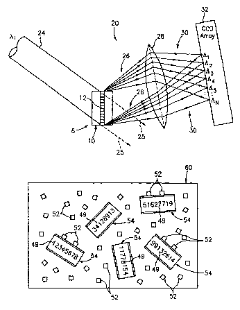
The incident light 24 of a wavelength ~,, e.g., 532 nm from a known frequency
doubled Nd:YAG laser or 632nm from a known Helium-Neon laser, is incident on
the
grating 12 in the substrate 10. Any other input wavelength ~, can be used if
desired
provided ~, is within the optical transmission range of the substrate
(discussed more
hereinafter).
A portion of the input light 24 passes straight through the grating 12 as
indicated by dashed lines 25. The remainder of the light 24 is reflected by
the grating
12 and forms a plurality of beams 26-36, each having the same wavelength ~ as
the
input wavelength ~, and each having a different angle indicative of the
pitches (Al-
An) existing in the grating 12.
As discussed hereinbefore, the grating 12 is a combination of a plurality of
individual spatial periods or pitches A of the refractive index variation
along the
substrate, each collocated at substantially the same location on the substrate
10
(discussed more hereinafter). The resultant combination of these individual
pitches is
the grating 12 comprising spatial periods (Al-An) each representing a bit in
the code.
Accordingly, the code is determined by which spatial periods (A1-An) exist (or
do not
exist) in a given composite grating 12. The code may also be determined by
arlrhtin"~t r,~,.~r.,e+o,." .,~ ...oll ,.,. .7:.,...........7
t.......:......p..._


CA 02496296 2005-02-18
WO 2004/019277 PCT/US2003/026316
The reflected light 26-36 passes through a lens 37, which provides focused
light beams 46-56 which are imaged onto a CCD camera 60. Instead of or in
addition
to the lens 37, other imaging optics may be used to provide the desired
characteristics
of the optical image/signal onto the camera 60 (e.g., spots, lines, circles,
ovals, etc.),
depending on the shape of the substrate and input optical signals. Also,
instead of a
CCD camera other devices may be used to read/capture the output light.
Each of the individual spatial periods (Al-An) in the grating 12 is slightly
different, thus producing an array of N unique diffraction conditions (or
diffraction
angles) discussed more hereinafter. When the element 8 is illuminated from the
side,
in the region of the grating 12, at the appropriate angle (discussed
hereinafter), with a
single input wavelength ~, (monochromatic) source, the diffracted (or
reflected) beams
26-36 are generated.
The beams 26-36 are imaged onto the CCD camera 60 to produce a pattern of
light and dark regions representing a digital (or binary) code, where light =
1 and dark
= 0 (or vice versa). The digital code may be generated by selectively creating
individual index variations (or individual gratings) with the desired spatial
periods
A1-An. Other illumination, readout techniques, types of gratings, geometries,
materials, etc. may be used as discussed in the aforementioned patent
application.
Referring to Figs. 3 - 7, the substrate 10 of the optical identification
element
(or microbead) 8 may functionalized by coating the substrate with a material
of
interest 50, which is then used in a chemical reaction or as an attractant for
certain
chemicals 52. This capability to uniquely encode a large number of microbeads
8
with a corresponding number of different substances or materials attached to
each
microbead enables these coated microbeads to be mixed with an unknown analyte
52
to perform a multiplexed experiment. The procedure 40 for performing such a
multiplexed assay or experiment includes the steps of producing 42 the probe
or
microbead 8, as described hereinbefore, and functionalizing 44 the outer
surface of
the microbead 8 by coating/depositing it with a material 50 that will react in
a
predetermined way with other chemicals/substances ~52. An assay is then
performed


CA 02496296 2005-02-18
WO 2004/019277 PCT/US2003/026316
46 with a plurality of microbeads with different identification codes 49 at
the same
time. In step 48, the fluorescence of the microbeads 8 is analyzed, and the
identification element 8 is read to determine the code of each microbead to
thereby
determine information about the chemical reaction.
In Fig. 4, a coated microbead 54 is shown, wherein the outer surface of the
microbead 8 is coated with a material 50 (functionalized) and used in a
chemical
reaction or as an attractant for certain test material 52 (see Fig. 5). The
coating
material 50 comprises a probe molecule or compound 56 attached to the
microbead 8
by a linker molecule or complex. The probe molecule 56 includes a molecular
group
55 for attachment to the linker molecule 58 and a molecule/compound of
interest 57,
such as an Oligonucleitides (oligos), antibodies, peptides, amino acid
strings, cDNA,
RNA, chemicals, nucleic acid oliorners, polymers, biological cells, or
proteins. For
example, the probe molecule 50 may comprise a single strand of DNA (or portion
thereof) and the test material 52 comprising at least one unknown single
strand of
DNA. As shown, the probe molecule 56 is attached or adhered to the outer
surface of
the substrate 10 by a linker molecule or complex 58. In some instances, the
molecule
of interest 57 of the probe molecule 56 may be attached directly to the outer
surface of
the substrate 10, or directly synthesized (or grown) onto the surface of the
microbead
8, such as via phosphoramidite chemistry. Examples of surface chemistry for
the
microbeads 8 include Streptavidin/biotinylated oligos and Aldehyde/amine
modified
oligos. Further, the microbead may be coated with blocker of non-specific
binding
(e.g., salmon sperm DNA) to prevent bonding of molecules (e.g. DNA) to the non-

functionalized surface 59 of the microbeads.
Refernng to Fig. 5, a plurality of functionalized microbeads 54 may then be
placed within a cell or container 60 to perform an assay. As discussed in step
46 of
Fig. 3, the functionalized microbeads 54 placed in the cell have different
identification
codes 49. Each identification code 49 corresponds to a unique molecule of
interest
57. For example, all functionalized microbeads 54 disposed within the cell
having an
identification code of 12345678 is coated with a unique molecule of interest
52, while


CA 02496296 2005-02-18
WO 2004/019277 PCT/US2003/026316
all functionalized microbeads 54 having an identification code of 34128913 is
coated
with a different unique molecule of interest.
The test material or molecules 52, disposed within a solution, are then
injected
into the cell 60 and mixed with the functionalized microbeads 54. The test
molecules
may include a single type of unknown molecule, or in most cases, the test
molecules
comprise a plurality of different unknown test molecules. During mixing of the
solution of test molecules 52 and functionalized microbeads 54, the test
molecules
attach to the complementary molecules of interest 57, as shown for
functionalized
microbeads having codes 12345678, 51627719, and 99132614. For example as
discussed hereinbefore, each coded functionalized microbead 8 has a unique
molecules of interest 57 attached thereto, such as a portion of a single
strand of DNA.
Similarly, the test molecules of the analyte comprise a plurality of unknown
single
strands of DNA. These test molecules 52 are also processed with a fluorescent,
such
as dyeing, such that the test molecules illuminate. As will be discussed
hereinafter,
the fluorescence of the test molecules 52 provide the means to identify, which
functionalized microbeads have a test molecule attached thereto.
Once the reaction or combining is complete, the functionalized microbeads 54
are rinsed off with a saline solution to clean off the uncombined test
molecules 52.
As shown in Fig. 6, the functionalized microbeads 54 may be placed in a tray
64 with
grooves 62 to allow the microbeads 54 to be aligned in a predetermined
direction,
such as that described in U.S. Patent Application Serial No. (Cidra Docket No.
CC-
0648), filed contemporaneously" which is incorporated herein by reference. The
grooves 62 may have holes (not shown) that provide suction to keep the
microbeads
54 in position. Once aligned in the tray 64, the functionalized rnicrobeads 54
are
individually scanned and analyzed by the bead detector 20.
As best shown in Fig. 7, each functionalized microbead 54 is detected for
fluorescence and analyzed to determine the identification code 49 of the
microbead
54. A light source (not shown) may be provided to luminate the rnicrobeads 54.
Once the fluorescent microbeads 54 are identified and knowing which single
strand of


CA 02496296 2005-02-18
WO 2004/019277 PCT/US2003/026316
11
DNA was attached to each coded micribead 54, the bead detector 20 determines
which single strands of DNA were present in the test material 52. As described
hereinbefore, the bead detector 20 illuminates the microbead 54 and focuses
light
reflected by the diffraction grating 12 onto a CCD array or camera 31, whereby
the
code 49 of the microbead is determined. Secondly, the bead detector 20
includes a
fluorescence detector 66 for measuring the fluorescence emanating from test
molecules 52 attached to the element 8. The fluorescence meter 66 includes a
lens 68
and optical fiber 70 for receiving and providing the fluorescence from the
test
molecules 52 to the fluorescence meter.
The invention may be used in many areas such as drug discovery,
functionalized substrates, biology, proteomics, combinatorial chemistry, DNA
analysis/tracking/sorting/tagging, as well as tagging of molecules, biological
particles,
matrix support materials, immunoassays, receptor binding assays, scintillation
proximity assays, radioactive or non-radioactive proximity assays, and other
assays,
(including fluorescent, mass spectroscopy), high throughput drug/genome
screening,
and/or massively parallel assay applications. The invention provides uniquely
identifiable beads with reaction supports by active coatings for reaction
tracking to~
perform multiplexed experiments.
Some current techniques used in combinatorial chemistry or biochemistry are
described in US Patent No. 6,294,327, entitled "Apparatus and Method foz~
Detecting
Samples Labeled With Material Having Strong Light Scattering Properties, Using
Reflection Mode Light and Diffuse Scattering", issued Sept. 23, 2001 to Walton
et al.;
US Patent No. 6,242,180, entitled "Computer Aided Visualization and Analysis
System for Sequence Evaluation", issued June 5, 2001, to Chee; US Patent No.
6,309,823 entitled "Arrays of Nucleic Acid Probes for Analyzing
Biotransformation
of Genes and Methods of Using the Same", Oct. 30, 2001, to Cronin et al.; US
Patent
No. 6,440,667, entitled "Analysis of Target Molecules Using an.Encoding
System";
US Patent No. 6,355,432, entitled "Products for Detecting Nucleic Acids"; US
Patent
No. 6,197,506, entitled "Method of Detecting Nucleic Acids"; US Pat No.
6,309,822,


CA 02496296 2005-02-18
WO 2004/019277 PCT/US2003/026316
12
entitled "Method for comparing copy number of nucleic acid sequences"; US
Patent
No. 5,547,39, entitled "Sequencing of surface immobilized polymers utilizing
microflourescence detection", which are all incorporated herein by reference
to the
extent needed to understand the present invention.
The invention can be used in combinatorial chemistry, active coating and
functionalized polymers, as well as immunoassays, and hybridization reactions.
The
invention enables millions of parallel chemical reactions, enable large-scale
repeated
chemical reactions, increase productivity and reduce time-to-market for drug
and
other material development industries.
The microbeads ~ are inexpensive to manufacture and the identification codes
49 are easy and inexpensive to imprint into the microbeads. The codes are
digitally
readable and easily adapted to optical coding techniques. Thus, the optical
readout is
very simple and inexpensive to implement. The code is not affected by spot
imperfections, scratches, cracks or breaks. In addition, splitting or slicing
an element
axially produces more elements with the same code; therefore, when a bead is
axially
split-up, the code is not lost, but instead replicated in each piece. Unlike
electronic ID
elements, the elements of the present invention are not affected by nuclear or
electromagnetic radiation.
The dimensions and geometries for any of the embodiments described herein
are merely for illustrative purposes and, as such, any other dimensions may be
used if
desired, depending on the application, size, performance, manufacturing
requirements, or other factors, in view of the teachings herein.
It should be understood that, unless stated otherwise herein, any of the
features, characteristics, alternatives or modifications described regarding a
particular
embodiment herein may also be applied, used, or incorporated with any other
embodiment described herein. Also, the drawings herein are not drawn to scale.
Although the invention has been described and illustrated with respect to
exemplary embodiments thereof, the foregoing and various other additions and


CA 02496296 2005-02-18
WO 2004/019277 PCT/US2003/026316
13
omissions may be made therein and thereto without departing from the spirit
and
scope of the present invention.

Representative Drawing
A single figure which represents the drawing illustrating the invention.
Administrative Status

For a clearer understanding of the status of the application/patent presented on this page, the site Disclaimer , as well as the definitions for Patent , Administrative Status , Maintenance Fee  and Payment History  should be consulted.

Administrative Status

Title Date
Forecasted Issue Date Unavailable
(86) PCT Filing Date 2003-08-20
(87) PCT Publication Date 2004-03-04
(85) National Entry 2005-02-18
Examination Requested 2008-08-19
Dead Application 2012-08-20

Abandonment History

Abandonment Date Reason Reinstatement Date
2011-08-22 FAILURE TO PAY APPLICATION MAINTENANCE FEE
2011-12-30 R30(2) - Failure to Respond

Payment History

Fee Type Anniversary Year Due Date Amount Paid Paid Date
Registration of a document - section 124 $100.00 2005-02-18
Application Fee $400.00 2005-02-18
Maintenance Fee - Application - New Act 2 2005-08-22 $100.00 2005-08-05
Registration of a document - section 124 $100.00 2006-05-16
Maintenance Fee - Application - New Act 3 2006-08-21 $100.00 2006-07-28
Registration of a document - section 124 $100.00 2007-01-22
Maintenance Fee - Application - New Act 4 2007-08-20 $100.00 2007-07-19
Maintenance Fee - Application - New Act 5 2008-08-20 $200.00 2008-07-15
Request for Examination $800.00 2008-08-19
Maintenance Fee - Application - New Act 6 2009-08-20 $200.00 2009-07-16
Maintenance Fee - Application - New Act 7 2010-08-20 $200.00 2010-07-14
Owners on Record

Note: Records showing the ownership history in alphabetical order.

Current Owners on Record
CYVERA CORPORATION
Past Owners on Record
CIDRA CORPORATION
CYVERA CORPORATION
ILLUMINA, INC.
MOON, JOHN
PUTNAM, MARTIN A.
Past Owners that do not appear in the "Owners on Record" listing will appear in other documentation within the application.
Documents

To view selected files, please enter reCAPTCHA code :


To view images, click a link in the Document Description column. To download the documents, select one or more checkboxes in the first column and then click the "Download Selected in PDF format (Zip Archive)" or the "Download Selected as Single PDF" button.

List of published and non-published patent-specific documents on the CPD .

If you have any difficulty accessing content, you can call the Client Service Centre at 1-866-997-1936 or send them an e-mail at CIPO Client Service Centre.


Document
Description 
Date
(yyyy-mm-dd) 
Number of pages   Size of Image (KB) 
Abstract 2004-03-26 2 73
Claims 2004-03-26 15 815
Drawings 2004-03-26 5 75
Description 2004-03-26 13 614
Representative Drawing 2005-02-18 1 17
Cover Page 2005-04-28 2 55
Claims 2005-02-18 15 1,031
PCT 2005-02-18 9 302
Assignment 2005-02-18 3 90
PCT 2005-02-18 22 1,375
Correspondence 2005-04-25 1 27
Fees 2005-08-05 1 32
Assignment 2006-05-16 18 1,137
Assignment 2007-01-22 19 577
Correspondence 2007-03-02 1 16
Assignment 2007-09-17 5 172
Prosecution-Amendment 2008-08-19 2 50
Prosecution-Amendment 2011-06-30 2 79