Note: Descriptions are shown in the official language in which they were submitted.
CA 02496569 1994-07-21
_ 1 _
RADIOTELEPHONE SYSTEM FOR GROUPS OF REMOTE SUBSCRIBERS
Field of the Invention
This invention relates to radiotelephone systems for
serving a plurality of remote subscriber stations and, more
particularly, to a radiotelephone system in which certain
of said subscriber stations are located in a physically
adjacent group.
Background of the Prior Art
A radiotelephone system including a base station for
serving remote subscriber stations is described in U.S.
patent 5,119,375. In that system each subscriber station
was equipped with a radio that could be instructed by the
base station to tune to a particular channel and to employ
a particular time slot for the duration of a given
conversation. Time division multiplex (TDM) radio channel
transmission was employed from the base station to the
subscriber stations and time division multiple access
(TDMA) transmission from the individual subscriber stations
to the base station. The time division of each radio
channel into time slots and the compression of speech
signals permitted each radio frequency channel to support
a number of voice paths equal to the number of time slots.
Analog voice signals to and from the public switched
telephone network were first converted to 64 kbps ~-law
companded pulse coded modulation (PCM) digital samples.
Before transmission over the radio channel the digital
samples were subjected to voice-compression to reduce the
voice information rate from 64 kbps to 14.6 kbps using
residual excited linear predictive (RELP) coding. A voice
codec and modem were required to be dedicated to a specific
frequency and time slot for the duration of a call.
While the foregoing system operated in a highly
satisfactory manner in allowing telephone service to be
provided especially to areas where wire lines are
CA 02496569 1994-07-21
=2-
impractical, the unforeseen growth of such telephone
service has given rise to situations .iii iahich several
subscriber stations are found to lie in close proximity
with one another. Initial efforts to lower the per-line
1 cost of serving a group of~such closely situated dubscriber
stations were focused on consolidating the installation and
maintenance costs of individual~subscriber stations~through
the sharing of common equipment such as the enclosure,
power supply, RF power amplifier and antenna. Thus, in a
l0 closely situated group of 'sub9cribet stations, each of
which could access an RF channel, a single broadband RF
power amplifier could, be erhployed ~ to ~ serve the group .
However such efforts still required~each subscriber line to
have its own modem anc~ radio transceiver.. ~ 'fhe individual
transceiver outputs were fed to .the common RF power
amplifier, iahich had to be~designed to handle.a peak power
equal to the sum of the power of ~11~ of the .transceivers in
the group of adjacent subecriber~~stations~~~that could
simultaneously be active on the~~same time slot. It is
2o apparent that further consolidation oyez that possible in
the '375 patent system and a reduction~in the~peak and
average power required would be desirable, especially in
remote areas required to be served by~solar cell power.
5ummary of the Invention
2 S - In accordance with the principles of our invention,
per-line costs are reduced for a physically adjacent groug
of subscriber lines by permitting~'the line s within such a
group to share not only a common povier~~supply and RF power
amplifier, but modem, synchronizativn,~ ,IF, up- ~~and down-
30 conversion and controller functions .as .well., eo that
significant concentration is achieved. , In our~system, a
small number o~ modems is provided ~to sex-ve. they multiple
subscribers in a physicallyadjacent group, hereinafter
:referred to as cluster or, more particillarly, as~a modular
35 r_luster. In an illugtratWe embodirrient, subscriber line
CA 02496569 1994-07-21
circuits and modems are modularized printed circuit cards
which plug into a frame employing backplane wiring to
distribute timing information and data among tine units.
Ar_y oz the modems may be seized to handle a call for any of
3 the subscribers and each modem may handle calls for several
subscribers on successive time slots. The same or a
different fretruency may be used to support communications
for each subscriber on successive time slots.
It is a feature of our invention that the selection
1o from the common pool of frequency-agile modems of the modem
to be used to handle a call is controlled to conserve power
consumption in two ways. First, a new modem is preferably
not seized tar use to handle a call until all oz thz time
slots on active modems have been assigned to calls, thereby
15 allowing all not-yet-selected modems to remain in a power-
conserving, "powered-down" state.
Second, the number of calls using the same time slot (on
different frequencies) is controlled to reduce the peak
power demand on the RF power amplifier.
20 It is a further feature of our invention to avoid
synchronization delay when it is necessary to seize a
nower2d-down modem for use on a call. Once time slot
synchronization with the base station has been established
for the first modem of the pool at the cluster,
25 synchronization information is made available to the
remaining modems, advantageously over backplane wiring,
under control of a microprocessor-based cluster controller.
.Accordingly, all powered-down modems remain instantly
assignable to handle calls without undergoing any delay to
30 become synchronized with the base station's time division
frame .
It is a further feature of our invention to classify
modem synchronization states according to several
synchronization parameters and to derive a confidence
35 factor for each active modem that reflects the reliability
of the synchronization parameters and to distribute
CA 02496569 1994-07-21
-4-
s~chtonizatiarl information from the modem ha~iihg the best
cdrifidence factor.
Brief Description of the Drawiricts
The foregoing and other objecta and features of our
invention inajr become more apparent by referring noiw to the
drawing in +ahich
Fig. 1, i9 a block diagba~tt of ~ modular cluster having
'a common pool of frequency agile modems' for handling a
group of subscriber stations; '
Fig. 2A shbws the asaoCiation'of subsdriber line
circuits and Modems at the time slat iriterchahger;
Fig. 2H shows the TDMA RF frame allocated for 15PSK
time s~.o~s
Fig. 2C shows the TDMA RF frame allocated for QPSK
time slots;
Fig, 2D shows the task scheduling between the TDMA
time slots and the PCM buffers;
Fig. 3 shows the principle circuit-elementB of a
frequency agile modem module;
z0 Fig. 4 shows the IF portion ofwthe frequency agile
modern ;
Fig. 5 is a bl ock diagram of the block synthesizer,
up/dowri converter;
Fig. 6 shows the frequency synthesis and noise shaper
for the receiver partibn of the modern;
Fig. 7 shows the frequency synthesis, modulation and
noise shaper circuitry for the IF'transmitter portion of
the modem; and
Fig. 6 shows the system clock generation circuitry for
3o the modular cluster.
General Description
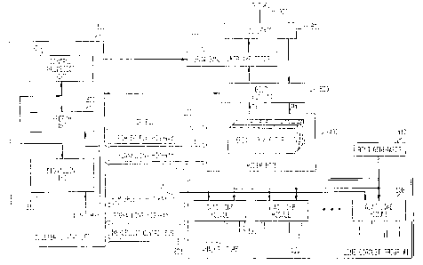
Fig. 1 is a block diagram of a modular subscriber
cluster that i9 located remotely from a base station (not
CA 02496569 1994-07-21
-
shown). The subscriber cluster is termed "modular" because
the line circuits 100 and the modems 400 are comprised of
plug-in units. Accordingly, the number of plugged-~r_
subscriber line circuits 100 will depend on the number of
subscribers in the locality and the number oz plugged-in
modems 400 may be traffic-engineered to handle the amount
of traffic expected to be generated by the number of line
circuits 100. Line circuits 100 are contained on quad line
module cards 101-108, each of which serves four subscriber
lines. Eight such cguad line modules provide loop control
functions to a line group of 32 subscriber lines and
circuits 100 may contain multiple line groups.
Each line circuit on each quad line module 101-108 is
given a dedicated PCM time slot appearance in PCM speech
highway 200 and in signaling highway 201. The quad line
modules 101-toe include voice codecs (not shown) to encode
subscriber loop analog voice onto PCM data highway 200.
Subscriber loop signaling information is applied to
sigr_aling highway 201 by a Subscriber line interface
circuit SLIC (not shown). Either ~C-law or A-law PCM coding
may be used.
The connection of a particular one of modems 400 to
handle a call from or to a particular one of the line
circuits on one oz quad ~ ine modules ? O1-108 is made via
time slot interchangers 310 and 320, as instructed by
cluster controller 300. PCM data time slot interchanger
320 conveys speech samples between the PCM speech highway
200 serving Iine modules 101-108 and the Pr'M speech highway
220 serving modem pool 400. Signaling time slot
interchanger 310 conveys signalling information between
signalling highway 201 serving the modules 100 and
signalling highway 221 ser~ring modem pool 400.
Two RF channels are required for a telephone
conversation, one for transmissions from the base station
t:o the subscriber (the 'forward' channel) and one from the
subscriber to the base station (the 'reverse' channel).
The forward and reverse channel frequencies ar= assigned by
CA 02496569 1994-07-21
-6-
the telecommunications authox'ity and in a typical example
may be separated from each other by S MHz. The path of the
forward channel radio signal~received at the cluster from
the base station may be traced ftotri cl~ieter antenna 900 and
. 5 duplexer 800 to block synthesizer up/down converter (BSUD)
600: In block converter 600 the RF signal i9 limited,
band-pass filtered and down-converted.from the 450 MHz, 900
MHz or othex high, or ultra-high frequency RF band to an IF
signal iri the 26 - 28 MF#z range. ~ The IF signal is
to delivered t-o modems 400 wh~.ch process the signal for
delivery to the subscriber lisle circuits via the time slot
interchangers in the cluster controller 30D:
. The moderrln each . inc~.i~de a basebahd ~ digital signal
processor (see Fig. 3, DSP/BB) and a fibde~i' ~roceseor (see
15 Fig : 3 , DSP/MDirI) : In tie forward chanriel direction; modem
processor DSP/M77M demodulates the IF signal received from
block converter s00 and transfers the data to baseband
processor DSP/HB which expands the demodulated data into c-
law or A=law eilcoded signals for transmission through time
20 slot interchanges 320 to the line modules: The modem's
baseband processor DSP/HB interfaces to modem processor
DSP/MDM vis. s. direct memoY-y access DMA) interface (see
Fig. 3) and to the PCM highways through the processor's
serial port. In the reverse channel-direction, baseband
25 processor DSP/BH conyterts the ~C=lawi~or A-law coded PCM
:inforcrtation received from PCM highway S00 into linear form,
cr5mpresses the linear data ~isirig ' ~ KELP coding and DMA
transfers the compte9sed data to digital signal processor
DSP/IKDM which modulates the signal for transmission on the
30 radio channel time slot,
As shown in Fig. 2A, each of modems 400 and each of
J.ine modules 100 has four dedicated time slot appearances
in PCM oats. time slot interchariger 320 for non-blocking
access. Each modem is assigned two adjacent PCM slots in
'35 PCM time slots 0-15 and two sdjacent PCM time slots in PCM
time Blots 16-31. Ag an example, for a particular call,
TSI 320 connects .line circuit 0 of line ' module 'ZO1 to
CA 02496569 1994-07-21
channel 1 of modem l, and line circuit 1 of line module 101
is connected to channel 0 of modem 1, and so on. Time slot
interchangers 310 and 320 provide a repetitive 125 ACS
sampling period containing 32 time slots operating at a
rate of 2.048 Mbits/sec. During each I25 ~S PCM interval,
the line modules may send thirty-two, e-bit bytes of data
to time slot interchanges 320 and each modem may receive
four of the 8-bit bytes at its baseband processor serial
port, packed together as two 16-bit words. Each 16-bit
word causes a aerial port interrupt on the baseband
processor. When the interrupt is received, the baseband
processor determines whether the pair of PCM samples
contained in the lo-bit word correspond to slots 0 and 1 or
to slots 2 and 3. Similarly, during each 125 ~.S PCM
interval, four voice channels of PCM data, packed together
as two 16-bit words, may be sent from each baseband
processor's serial port to time slot interchanges 320 for
delivery to the line modules.
The TDM (RF) frame at the base station is shown .n
Figs. 2B and 2C, each having a duration, illustratively, of
45 ms. The 16PSK frame of Fig. 2B has four time slots,
each of duration z, each time slot capable of carrying the
different frequencies assigned to the forward and reverse
channels of the call. zn Fig. 2C the RF frame of the same
duration is capable of accommodating the forward and
reverse channels of two QPSK modulated calls. It can be
appreciated that, alternatively, the TDM frame can carry
four 16PSK calls or two QPSK modulated calls.
Fig. 2D illustrates the timing of the tasks performed
at the cluster in conveying information between an
illustrative TDMA frame carrying QPSK modulated calls and
the PCM highway frames. Line (1) represents the buffers f or
receiving the two QPSK modulated forward channel time
slots, Rxl and Rx2, of th= TDhL~. frame. Demodulation is
begun as soon as the receive buffer has received the first
half, Rxla, of the time slot. Line (2) represents the
buffers preparing, to transmit i n the two reverse charnel
CA 02496569 1994-07-21
-8-
QPSK tittle slots, Txl and TX2, of a TDMA frame: Note that,
at the Cluster, the re~ierse channel time slots are offset
from the forward channel time slots so that the et~bscriber
station may avoid the expense and bulk of a duplexer. In
addition; the subscriber unit's the reverse channel will be
offset so that it will be received at the base station at
the pxoper time taking into account 'the' distance between
the stibscribet station and the base station, Lines (3) and
(4) of Fig, 2D represent the buffers in the.SRAM (Fig. 3)
of the modem -which store the PCM 4rords to arid from speech
dime slot interc:hanger TSI 320 (Fig. 1) .
In normal voice operation, the modem processor DSP/MDM
demodulates received forward channel symbols, packs them
into a buffer ~.n SAAM/MDM and sends the contents of the
buffer to the baseband processor DSP/BB for R.ELP synthesis
(expansion): The baseband processor encodes the expanded
data to ~t-lad or A-late arid pots it on the PCM bus for
delivery to the line motiuleg. 'Voice code words are
r_ransc~litted iii every frame during active vbice operation .
The code Word resides at the beginning of the burst between
the treamble and voice data on both the forward and reverse
channels. The forward channel voice code words contain
j.nformation that may be aged to adjust transmit power and
timing. Local loop control information (i.e.,~ onhook,
offhook, ring, forward disconnect) .'is also embedded in
these code words. The reverse channel code words contain
subscriber station local loop control and forward channel
link quality irlforination.
The forGiard ttoice codewotcl i9 decoded by the modem
3p processor DSP/MDM. The forward voice codeword contains
transmit frs:ctional timing control,'txansmit power~level
control and local loop .control information: The fractional
timing and power level control information is averaged out
over a frame and the average adjustment made at the end of
the frame. The local loop control information is stored
locally and changes in loop state axe detected and reported
to the cluster controller. The local loon control also
CA 02496569 1994-07-21
-9-
causes the modem to send out line circuit control over the
signalling bus. The reverse voice codeword contains local
loop status that is used by the cluster controller and base
station to monitor call progress.
The modem processor DSP/MDM performs receive FIR
=altering and automatic gain control of the received
samples during a receive symbol interrupt servzce routine,
The demodulator routine in the modem processor is called
when half a slot of baseband information has been received
to in the receive buffer. The demodulator operates on the
half slot of data and passes the packed output data to the
baseband processor DSP/HB for KELP synthesis. Data
transfer to and from the baseband processor is controlled
so that the RELP input queues are filled before the
corresponding synthesis data is required, and KELP output
rnzeues axe emptied beTare new analysis (compression) output
data arrives. During demodulation, automatic frequency
control (AFC), automatic gain control (AGC) and bit
tracking processes are performed to maintain close
2o synchronization with the base station.
It should be appreciated that mixed mode operation is
possible whereby some time slots in the RF may employ lo'PS~C
modulation while the remaining slots employ QPSK
modulation.
Synchronization to the Base Station
Before an RF channel can be used for communication
between the base station and the cluster, the cluster must
be synchronized to the RF time slot scheme used by the base
station (not shown.?. In accordance with our invention, one
3p or more of modems 400 will be ordered by cluster controller
3c)0 to acquire synchronization with the base station RF
frame timing by searching for the channel frequency
carrying the radio control channel (RCC) being used by the
base station. Cluster controller 300 includes a master
control microprocessor 33Q, illustratively, one employing
CA 02496569 1994-07-21
-10-
a Motorola 68000 series processor, which ~e~ndg~ control
information over the CP btts to the fiic~oprocessors in
modems 400. On power trp, cluster controller 300 down-loads
appropriate sofr_ware and initialization data to modems 400.
After the channel frequency is found; the modem must
synchronize with the base station time slot by decoding the
ACC unique word: As described in the aforementioned '375
patent, the ACC channel is distinguished from other
channels in that it has an extended guard interval: during
its time elot.and includes a DBPSK modulated'unique word of
8 bits. In order to minimize the possibility of aborting
a call if the modem with the active RCC time slot fails and
it becomes necessary to assign the RCC time slot to a
different modem, time slots are assigned Within an active
modem eo that th<s synchronization (ACC) time slot (referred
to as Rx0 where the four time slots axe numbered.RxO
~throughv Rx3, or FtxZ. where. the ' time slots are number Rx1
through Rx4)s is the last to be~filled:
At start-itp, all of tnoderrl9 400 are assumed to be out
of synchronization with the base station' a RF 45 Iris frame .
l7uring tune slot zero of the RF frame,~the base station
transmits an RCC message on some RF channel which;'when
received at the modular cltister,~will be decoded to~put the
cluster into synchronization with the base station's RF
time slot frame fox all RF channels. Until synchronization
with the base station is achieved, eaoh modem generates its
own local RF frame sync. Cluster controller 300 next
c:omrnands one or more rirodercis to hunt for the RCC transmitted
by the base station on different RF tharinel~ until the RCC
i.s found or 311 channels have been ~sea~thed, If all
channels have been searched and the RCC has not been found,
the controller orders the search to begin again.' When a
ii~odem finds the RCC, the controller designates it ~ as the
RCC modem and distributes its sync inforni~.tion to the
rernairiirig modems via the frame sync signal over the
backplane:
CA 02496569 1994-07-21
-11-
When the RCC slot search is undertaken, the channel
number is used by the modem to digitally sweep a d=rest
digital frequency synthesis tDDFS) local oscillator,
illustrativel y over a 2 1~-~z range . There are two stages to
a modem's ac~sisition cf the RCC channel, coarsely
identizying the center frequency and finding the "AM hole",
a portion oz the: RCC time slot where the number of symbols
transmitted by the base station does not fill up the entire
slot time. Coar9e frequency acquisition is based on
to performing a Hilbert transform of the spectrum of the RCC
channel which yields a frequency correction for the loczl
oscillator. This continues until the energy in the upper
half of the spectrum approximates that in the lower half.
After coarse frequency acquisition is obtained,
'15 illustratively t:o within an accuracy of 300 H2 of the
channel center f:reauency, a search is made for the AM hole .
A number of null signals are transmitted prior to the RCC
data. The AM hole is identified by monitoring the
amplitude of consecutive received symbols. When twelve
20 consecutive null symbols are detected, an AM strobe signal
is output by the modem to indicate the start of an RCC slot
and the start of a TDMA frame. This coarsely synchronizes
the baseband modem timing to the base station timing.
:>ynchronization need only be performed once since the radio
25 link is shared by all baseband modems in the modular
cluster. The frame sync signal is sourced by one modem to
all other modems in the cluster via a signal on the
backplane wiring. During the search for the RCC if the AM
hole is found to within 3 symbol periods of the start of
30 frame marker, coarse acquisition is complete. The location
of the unique word within the frame provides the modern with
taming infornation that is used to bring the modem's local
frame timing to wi_thi.n one symbol timing of the base
station. The modem is said to be in receive sync, Rx RCC,
35 as long as it continues to receive and decode the u_n~crue
word correctly. Once synchronization is achieved, l6pSK
modulation corresponding to 4 bits per symbol, QPS~C
CA 02496569 1994-07-21
-12-
mod~ilation cotrespond3ng to 2 bits pez symbol, or
combinations of both may be employed.
While all modems are capable of receiving and
synchronizing to the base station's radio control channel
RCC, only one modem need do this since the modem which is
selected by the cluster Controller can share its timing
with the other modems via the Frame Sync signal over the
backplane wiring. The selected modem will source the Frame
Sync Out ~igi~~l and all other modems will. accept this
signal as the Frame Sync In signal.
When a modem goes on line, its modem processor DSP/MDM
instructs its DDF 450 (Fig. 3 ) to try to synchronize its
local frame timing to the backplane signal. Each modem's
DDF 450 timing :iB at this moment independent of every other
modem's timing. DDF 45o will initially be ingtructed~by
its DSPjt~M tt~ look at the backplane signal for its
synchronization., If a backplane eynchronizatiori signal is
present, the DDf will synchronize its~frame sync signal to
the backplane signal and then disconnect from the backplane
signal. The backplane signal, thus does not feed directly
into the modem's timing circuitry .but merely aligns the
modem' s internal start of recef~re frame signal . If a
backplane synchronization signal was not present, it is
assumed that the ciiodem is the first one that has been
activated by the cluster controller, in which case the
cluster controller 3170 will instruct the modem processor
DSP~MDM to look for the RCC and send the modem's timing to
the cluster Controller.
Cluster conttoller 300 next instructs the modem
processor DSP~MDM to demodulate the DBPSK signal on the RCC
~h~ai. The path for demodulation of the ~IF signal
:.-eceived ~ from bloc3c converter s0a may be traced to the
modem IF module where it is again band-pass filtered anti
down-converted to a 16 kilosymbol peg second information
stream. The DHPSK modulation that is employed on the RCC
channel is a one bit per symbol modulation. 'The RCC
messages that are . received from the base station must be
CA 02496569 1994-07-21
-13-
demodulated and decoded before being sent to the cluster
controller. Only messages that are addressed to the
cluster controller, have a valid CRC~and arm a burst type
message or an acknowledgment message are rorwarded to the
controller. All other messages are discarded. An
acknowledgment message signifies the correct reception of
the previous RCC message. A message is addressed to the
cluster controller if the Subscriber Identification number
(SID? contained in the message matches the SID of the
?o cluster.
Referxing to Fig. 3, the 16 kilosymbol per second IF
signal from the IF circuitry of Fig. 4 is entered into A/D
converter 804, which is sampled at a 64 KHz rate by a clock
signal received from DDF c:nip x50. A/D converter 804
performs quadrature band-pass sampling at a 64 kHz sampling
rate. Quadrature band-pass sampling is described, inter
olio, in US patent 4,784,9x0. At its output, converter 80Q
provides a sequence of complex signals which contains a
certain amount of temporal distortion. The output of
converter 804 (Fig_ 8? is entered into R.~cFIFO in DDF chip
450. Modem processor DSP/MDM reads the contents of R.~cFIFO
and performs a complex FIR filtering operation, which
removes the temporal distortion introduced by the
quadrature band-pass sampling. After the removal of
temporal distortion, the signals are demodulated by
procssor DSP/MDM.
During the demodulation of RCC messages, AFC, AGC and
bit tracking processes are perfomed by modem processor
i)SP/MDM to maintain the cluster in close synchronization
with the base station. Transmit timing and power level
adjustments axe made according to information received in
the RCC message.Processor DSP/MDht examines the
demodulated data and detects the RCC message, a message
v~hich includes link status bits, and 96 bits os data that
3S includes the subscriber ID. Modem processor DSP/MDM also
recognizes whether the subscriber ID belongs to one of the
subscriber line e~ircuits in the cluster.
CA 02496569 1994-07-21
-' 4 -
~f, ,the fiessage ~ is fot~ this - cluster ,"'the ~ me~shge is
passed to clugtet controller 300, Which intef-prets~the RCC
command. Fo~-vrard RCC meesageg include page ines9age~, a call
connect, clear indication and'self=test. Ftever'se RCC
S messages include call accept, clear request,'test results
and Ball reqtieet: If ~ the RCC message is 'a~ page message;
the cluster controller for t~ihich it ' is ~ designated will
formulate a call accepted megeage to be~transmitted back to
the base station: From the call accepted inAssage the base
station determines the timing offset between the cluster
and the basal Station and the base station'sends symbol
timing update information tv the cluster in the next RCC
meg5age, which is the call connect message:
When the RCC message is a call connect message, the
' information therein instructs the cliiste~ controller what
adjustment to make in symbol timirig~' whether to adjust
power level, fractional timing, and what channel to use for
the remainder of the call (chanizel~ htimber, TDM slot number,
whether QPSK or 16PSK tnodtilatiori wi~l be employed 'and what
the subscriber line tyoe'isj: ~ ~ ' '
The first modem which has found the RCC~is designated
the RCC modem and its freqiierity offset ~ ' receive gain
control Rx AGC, and start 'offrame information is
r_oiusidered valid and may be digt~ibi~ted to the w other
modems. The cluster controller receiires'the charinel riumber
information and decides which modem is to be inJtxLtcted to
tune uD to the designated chanriel''to'handlw the'remainder
of the call.
The final ~ step toward total" g~rnchronization is the
si.icceasful eatablishinent of a voice Channel. When a'voice
c:hanriel is established the last ~ ~ two 'gynchronixation
parameters becoma valid' the transmit,gymbol timing and
transmit symbol fractional tithing, At this point;'should
another modem be activated by the clUSter'eontYoller all of
the necessary syrichronization iriforfriation 'i5 aztailable to
be provided to the fiodem, making the establiehrnent'of a
voice channel much, easier and clicker _ A corlfidenee level
CA 02496569 1994-07-21
is calculated to evaluate the synchronization information
of each modem. The cluster controller updates the
confidence level for each modem whenever there is a c~.ange
in sync status, link quality, or receive AGC. The cluster
controller finds the modem with the highest confidence
level and distributes its synchronization parameters to the
remaining modems.
When a modem slot is commanded to enter the voice mode
by tile cluster controller, the modem. first attempts to
perform refinement. Refinement is the process of finely
synchronizing the modem's transmit timing and power level
to the base station's receive timing. The refinement
process is controlled by the base station. The base
station and the modem exchange special refinement bursts
?S until the base station terminates the refinement process
when the predetermined degree of synchronization has been
achieved. The modem then goes into normal voice operation.
If the base station aborts the refinement process, the
modem will abort the call, go into the idle state and
inform the cluster controller. Refinement bursts are DHPSK
bursts formatted like RCC bursts. Refinement bursts are
detected by the presence of a u~-iique refinement word. The
modem is said to be in voice synchronization when the
:refinement unique word is detected with zero offset. The
rorward and reverse voice codewords have a voice codeword
cheek byte attached for error detection. The modem will
report a loss of sync if 9 consecutive frames are received
with voice codeword errors, at which time the cluster
controller enters the recovery mode until a good codeword
is found or until the modem is commanded out of this mode
and placed into idle mode.
Based upon the synchronization state, duster
controller 300 determines the validity of the
synchronization parameters provided by the modem. The
table below shows which parameters are valid, based upon
the current synchronization state of a modem. An "X" in
the box indicates that the parameter is valid.
CA 02496569 1994-07-21
-16-
Sync State Freq, Sy bol Fract. TxPLC flxAGC SORE
Offset Time Time
No sync
px Sync(RCC) X ~ ~~ X X
Tx Sync (RCC)X X X X
Voice sync X X X X X X
A 12-bit confidence factor word is computed by the
modem to reflect the reliability of the synchronization
parameters ascertained by the modem. The confidence factor
word is assembled by concatenating the bite representing
the voice and receive sync states .of the modem with bits
identifying the link quality and receive AGC parameters,. as
set forth in the following table:
Bic Allocation 11 10 _ g.:9 7..0
Field Voice SyncR~ SyriC{'ftCC)Link Qw~lityluAGC
The single bits 11 and to identify, respectively,
whether or not, the modem is in voice'sync and receive sync.
The two bits 9 and a identify'four~gradations of link
quality, while the a bits allocated to receive AGC level
indicate the 7.evel of gain required:
MODEM MODULE, FIG: 3
The principle components of the modem module are shown
in Fig. 3. The modem module 'den support up to four
simultaneous full duplex voice channels. The processing to
dynamically handle all functions required by an active
channel is partitioned bet~tedn the ' ~ cluster controller
processor 320, (Fig: i), and proce9sors D~P/MDM and DSP/BB
in each modem (Fig: 3).. The cluster controller handles
higher level functions inclildihg call set~f~p, channel
allocation and system control: '~ Modem ~roCessor DSP/MDM
CA 02496569 1994-07-21
-i~-
handles filtering, demodulatior_ and routing of the incoming
radio signals,, formatting of data before transmission over
the radio channel, and managemer_t of data flow between
itself and baseband processor DSP/BB. Baseband processor
DSP/BH performs the computationally intensive tasks of
voice compression and expansion and, in addition, handles
the PCM bus interface. In normal voice operation, modem
processor DSP/MDM demodulates received symbols, packs them
into a receive buffer and sends the voice data buffer to
to baseband processor DSP/BB for KELP synthesis and
transmission to the subscriber 1 ine c~'_rcuit over the PCM
bus. The modem processor DSP/MDM also accepts compressed
speech from baseband processor DSP/BB, formats it into TDMA
bursts and sends it to the transmit pulse shaping filter
FIR contained in DDF 450 for transmission over the radio
link. The modem operates on both QPSK and 16PSK
modulations (and DBPSK during refinement) under~control of
the cluster controller.
Processors DSP/H$ and DSP/MDM each have a dedicated
random access memory, SRAM/MDM and SRAM/BB, respectively.
However, modem processor DSP/MDM may request access to the
random access memory SRAM/BB by activating its DMA HOLD
output and obtains such access using the data and address
bus when the baseband processor DSP/BB activates its DMA
ACK output signal.
Assignment of Time Slots
As described in the '375 patent, the RPU in the base
station keeps track oL.the radio channels and time slots
that are in use and assigns both the frequency and the time
slot to be used on any call. A slot is selected which is
in use by the least number of calls so that the call
traffic can be more evenly distributed across all slots.
However, in accordance with that aspect of the present
invention which is concerned with minimizing the power
expended at the remote modular cluster, calls are assigned
CA 02496569 1994-07-21
-18_
so as to (a) minimize the number of active modems and (b)
control the number of conversations simultaneously using
the same time slots. Further, while it ie desirable to
employ 16PSK modulation in every time elot.of a TDMA frame
S so that four complete calls can be accommodated, it i9 also
important to permit QPSK calls to .be made and to keep an
alternate RCC slot available for synchronization purposes.
Accordingly, the cluster and the base station must
. cooperate in the assignment of tide slots to achieve these
l0 goals. The cluster keeps track of available time slots and
the type of modulation being.employed on each slot, The
clustex then assigns priority levels to each available slot
and maintains a matrix of priority values Which takes into
account the factors that (a) an alternate receive time slot
15 (generally the first time slot) on.some channel must be
allocated for RCC synchronization, (b) adjacent time slots
should be left available as long as possible so that QPSK
calls can be handled if necessary, and (c) time slots
should be assigned to handle calls ,without, if possible,
20 activating a powered-down modem or assigning a slot that is
already in use by a large number of other calls: The
routine (in pseudo code) for achieving these goals is as
follows:
Prioritize Slot Routine
2 5 ~ List 1 = ail Idle time slots available on already active modems for
l6fSK cabs
and CtPSK calls;
Llst 1 A = ail idle modems;
Last 2 = Llst time slots whose usa wIU not exceed the thfeshhold number of
caNs using the same tlme slot In the cluster;
3 0 ~ List 2A = List 1 minus Llst 2;
List 3 = Llst 2 minus tlrna slots on modems having adjacent ,time slats
available (for QPSK calls);
List 3A = List 2 minus time slots on modems not hevlng adJacent time slots
available (lor OPSK caNs);
CA 02496569 1994-07-21
_~9_
List 4 = List 3 minus time slots on modems not having a synchronization time
slot available (slot 0 for the RCC);
List 4A = List 4 minus tirne slots on modems having a synchronization time
slot
available;
S ~ Mark list 4 as first choice;
Mark list 4A as second chaise;
Mark list 3 as third choice;
Mark list 3A as fourth choice;
Mark list 2 as fifth choice;
~ Mark list 2A as sixth choice;
Mark list 1 as seventh choice;
Mark list 1 A as eighth choice.
The above Prioritize Slot Routine is called whenever
the cluster receives an RCC page message from the base
station or is about to formulate a call request Message to
the base station. When the base station responds with a
call conr_ect message containing the frequency, type of
modulation and time slot to be used, the cluster once again
performs the Prioritize Slot Routine to see iz the slot
selected by th~~ RPU is still available. If still
available, the s:Iot is assigned to the call. However, if
in the meantime the slot assignments have changed, the call
will be blocked.
An example of how the Prioritize Slot Routine is
executed under light and heavier traffic conditions may be
helpful. Consider first the following table, wh~.ch
illustrates a possible condition of the modems and assigned
time slots under light traffic conditions, just before one
of the subscribers served by the modular cluster initiates
a request for service:
CA 02496569 1994-07-21
-20-
Modem Tune slot
0 1 2 3
0 RCC 16PSK
1 16PSK ~PSK ~ QPSK
2 1QLE IDLE tOLE IDLE
3 ' ' ~ '
, . . .:
-, . , , , .
The above table indicates that modem 0 has slots 2 and
3 available, that modem 1 has slot 1 available and that
modems 2, 3 , 4 and 5 are powe=ec~-doi~rri, all of their : time
slots being idle. The cluster executes the Prioritize'Slot
Routine which determines that slots 1, 2 and 3, in that
order, are the preferred slots to be assigned to.handle the
next 15PSK call and that for QPSK calls the preferred slots
are 2 and 0, in that order. The cluster then seride ~ "call
request" signal to the base station using the RCC Word and
irifornis the b~.se station of this preference . In .the table
below the rationale for esch o~ ~h.e priorities is set
forth
0 Slot PriorityRationale Slot Priority,Rationale
2
161'SK CIpSK
1 No new modems to power2 (Same reason
up; as
no livcrdas~ iri ~x ~ lBfSK for
slot activity; slots
OPSK slots 2.3 kept 2,3)
available;
RCC strut available.
2 New t7PSK call requires0 Requites new
new
modem power up. ~ modern power
up
3
~ D ~ Requires new modem
power up. I
Another example may be helpful. Consider the status
of time slots among modems 0-5 under somewhat heavier
traffic conditions, as shown in the following table,
wherein empty boxes indicate idle time slots'
CA 02496569 1994-07-21
-21-
Modem Time Sfot
1 ~ 2
0 RCC 16PSK aPSK QPSK
1 QPSK QPSK 16PSK
16PSK 16PSK 't 6PSK
3 I t3PSK QPSK QPSK CPSK
4 16PSK 16PSK IsPSK
S ~ ~ 18PSK
The slots to be assigned are set forth in the
following table together with the rationale:
Slot PriorityRationale Slot PriorityRationale
18PSK t~PS K
3 No new modems to power 2 only choice
up;
max slot activity avoided;
C1PSK slots 2,3 kept
available;
RCC slot kepi available.
2 No new modems to power
up;
max slot activity avoided;
RCC slot kept available,
BUT,
new C~PSK call requires
new
modem power up.
1 No new modems to power
up;
QPSK slats 2.3 kepi
available;
RCC slot kept available,
6UT
max slot activity exceeded.
1 S 0 No new modem power up;
QPSK slots 2.3 ksptavaitable;
BUT both max slot activity
exceeded and RCC slot
not kept
available.
rJp/Down Converter 600
In Fig. 5, i=orward channel radio signals Lrom the base
station are received in up/down converter 600 zrom the base
station via duplexer 800. The received RF signal is passed
through low-noise amplifier 502,, band-pass filtered in
CA 02496569 1994-07-21
-22-
filter 503, subjected to attenuation in attenuator 504 and
applied to mixer 505, where it is subjected to a first
down-conversion from the 450 MH2 RF band or the 900 MHz RF
band to an IF signal in the 26 - 28 MHz range. The IF
signal is passed through amplifier 506, bandpaes!filter
507, amplifier 508 and attenuator 509 and applied to
eplitter circuit 510 for delivery to the common pool of
modems. ' '
THe reverse channel modulated IF signals from the
20 common pool of modems are applied to combines 520 of block
up/dovm converter 600 at the upper left-hand corner of Fig.
5., subjected to attenuation in attenuator 521,~band-pass
filtered in band-pass filter 522, amplified in amplifier
523 and applied to mixer 525; where the signal is up
~ converted to an RF .signal .in either the 450 MFi~ RF band or '
the 900 MHz RF band. The RF signal is then~~etibjected to
attenuation in attenuator 526, band=~iae~ filtered in band-
pass filter 527, amplified in amplifier"528 and applied to
broadband highpower amplifier-700 which 'ends the signal on
to duplexes 800.
Mixers 505 and 525 receive their reference frequencies
from RxPLL pha9e locked loop circuit 540 and TxPLL phase
lock loop circuit 550, respect~.velji; ~haee locked loop 540
generates a 2 .36 MHz receiiie ~ lc5cal oecil~ator 'signal from
the signal provided by 21.76 Mf3z masterlclock 550, divided
by 2 and then by 8. The 1:35 ~iFi~ ~i~nal furnishes the
reference input to phase comparator~PC~vThe other input to
the phase comparator is providec~.b~ a feadback loop which
divides the output of circuit '540 by 2' and then by 177.
Feeding~back this signal to the phasa~comparator causes the
output of circuit 540 to have a frequency that is 354 times
that of the reference input, or 981.4 N~F3~. ~ The 481.44 M~iz
output of receive phase locked loop RxPLL 540 is applied
as the local oscillator input to down-conversion mixer 505.
. The 481.44 MHz output of circuit 540 is also applied
as the reference input for circuit 550, so that circuit
550 is frequency. slaved to circuit 540.' Circuit 550
CA 02496569 1994-07-21
-23-
generates the transmit local oscillator signal, which has
a frequency o:~ 4H1 . 44 MHz + 5 . 44 MI~z, i . a . it has a
frequency that is offset 5.44 !~IHz hig:-~er than the receive
local oscillator. For circuit 550, the 21.76 MHz signal
from master clock 560 is divided by 2, then by 2 again, to
make a signal. having a frequency of 5.44 MHz, which is
presented to the reference input of phase comparator PC of
circuit 550. The other ir_put of phase comparator PC of
circuit 550 is the low pass filtered difference frequency
l0 provided by mixer 542. Mixer 542 provides a frequency
which is the difference between the receive local
oscillator signal from circuit 540 and the vC0 output
signal of circuit 550. The output of circuit 550, taken
from its ir_ternal VCO is a frequency of x81.44 MHz + 5.44
M_s-Iz _
Fis. 4 IF Portion of Modem
Fig. 4 shows the details of the IF portion of tile
modem board in relation to tine digital portions (whose
details are shown in Fig. 3). At the lower right hand side
of Fig. 4, the receive IF signal from B5UD 600 (Fig. 1) is
applied through the lower terminal of loopback switch 402
to 4-Dole band-pass filter 404 whose a passband extends
from 20' to 28.3 MHz. The output of filter 404 is then
amplified by amplifier 406 and down-converted in mixer 408
which uses a receive local oscillator signal having a
freauency of between 15.1 MHz and 17.4 MHz: The output of
mixer 408 is amplified by amplifier 410, and filtered by 8-
pole crystal filter 412 whose center frequency is 10.864
MHz. The amplitude of the signal at the output of filter
412 is controlled by AGC circuit 414. The gain of AGC
circuit 41a is controlled by the VAGC signal from DDF ASIC
450 of Fig. 3. The output of AGC circuit 414 is then down-
converted by mixer 416, using a rezerence frequency of
10.88 h'Lf-Iz, to produce a 16 kilosymbol per second sequence
of IF data, wh_i.ch passes through amplifier 41B and is
CA 02496569 1994-07-21
-24-
delivered to the Rx IF input port of the circuitry of Fig,
3.
Still referring to Fig. 4, the circuitt-y of Fig. 3
generates a receive local oscillator signal, Rx DDFS, which
is filtered by ?-pole filter 432; then ~amDlified by
amplifier 434. The output of amplifier 434 is again low
pass filtered by ~-pole filter 436, ~whose~ output is
amplified by amplifier 438, then mixed with the received IF
radio signal in mixer 408.
At the- right hand side o~ Fig. 4,~ amplifier 420
received a master oscillator signal having a frec~.tency of
21.76 MHz arid applies the 21.76 MHz signal to splitter 422.
One output of splittex~ 422 i5 doubled infrequency by
frequency doulaler 424, twhoae autput~ is clipped in clipper
425 and shaped to TTL by gate 428, and inverted again by
gate 430. The output of gate 430 is applied to the inset
circuitry of Fig. 3 as a 43 ~ 52 MHz referehce clocl~ signal .
The other output of splitter 422 is passed through
amplifier 454 and attenuator 455 azid applied~to the local.
oscillator (L) input of mixer 444. Mixer 444 yip=Converts
the modulated IF signal, Tx DIF, from in~et~Fig, 3 after it
has been io~t pass filtered by filter 440 and attenuated by
attenuator 442.
The output of gate 428 also connects to the input of
inverter 460, whose output is frequency divided by 4 by
divider 462 and then uded as a loCa1 oscillator to down
convert the output of AGC block 414 in mixer 41d.
A loopback function is~ prodded by the serial
combination of sviitches 450 and 402 ~~.nd diimrn~ load 458 so
3 0 so that signals from the Tx DID' ouput ' ~ o~ the inset
reference to the circuitry of Fig. 3~may be looped back to
its Ftx zF input for teat purposes when training sequences
are applied to compensate for signal di9tortions; s~lch as
that occuring within crystal filter~412.
Still. referring to Fig. 4, the circuitry of rig. 3
provides a modulated IF output, at a frequency of 4.64 to
6 _ 94 ~ NIF-iz, which ,is filtered by 7-pole filter 440 and
CA 02496569 1994-07-21
-25-
attenuated by attenuator 442. The output of attenuacor 442
enters mixer 444, where it is up-converted to a frequency
in the range of 26.4 MHz to 28.7 Muz. The output of mixer
444 enters amplifier 446, whose output is filtered by 4-
pole bandpass filter 448 and applied to switch 450, which
is controlled by the loop-back enable output LBE of the
inset circuitry of Fig. 3. when loop-back testing is
conducted lead hBE is energized causing switche 450 to
connect the output of filter 448 to the top of dummy load
458 and energizing switch 402 to connect the bottom of
dummy load 358 to bandpass filetr 404 for loop back
testing. Loop-back testing is used with modem training
seauences to compensate for signal distortions within
crystal filter 412 and in other parts of modem circuitry.
When loop-back testing is not being conducted, the
output of switch 450 is applied to programmable attenuator
45z which may be programmed to one of 16 different
attenuation levels by the transmit power level control
signal, Tx PLC, from the inset circuitry of Fig. 3. The
output of attenuator 452 comprises the Tx IF PORT signal
that is applied to the upper left-hand side of the HSUD,
rFig. S.
Ficx. 6, RxDDS G~npration of Dia~ tal IF for Receive
Channels
The exact intermediate frequency to tune to to for a
receive time slot is determined when the cluster controller
CC (Fig. 1J tells the modem which RF channel to search for
the RCC message. During reception of the RCC message, fine
tuning of frequency anti timing is performed. The fine
tuning is accomplished at the IF level using phase
accumulator circuitry in tie RxDDS circuit of the mocnm's
DDF (Fig. 3), shown in detail in gig. 6. The IF
rrern_~encles are generated by repetitively accumulating, at
the frequency of a digital IF master clock, a number that
represents a phase step in the phase accumulator. Modem
CA 02496569 1994-07-21
-26-
processor DSP/~LD~t, via D5P/MDM data bti9 (fig. 3) , initially
furnishes ~. 24-bit number F to~ the f~xDDS ci=cLtiti-~r. This
number is related (as Will hereinafter be ~c~eecribed) to the
desired IF frequency required to demodulate ~ particular
incoming signal on a slot by slot bseis. ' The 2~-bit number
F is loaded into one of the four registers R16-Ft45 at the
lefthand side of Fig. 6. Iri the illustrative .einbodirnent
where s. 1,6-bit. processor is employed, the 24-bit frequency
number _F is supplied iri 16-bit and~8-bit segments, however,
to simplify the drawing, ~ the ~24-bit number is shown as
being entered into a composite 24-bit register: Each of
registers Rls-R46 ie dedicated to one of the receive time
slots. Since the RCC message is expected in the first Rx
time slot, the 24-bit number is loaded into the
corresponding one of the four registers R16.-R46, e.g.,
register R16. At the appropridte slot count for the first
Rx tune slot, register Rls'8 ~contenta~are presented to
synchronization register 602, whose output is then
presented to the upper input of adder 604: The~output of
adder 604 is connected to the input of ecciim~i~.ator register
606. The Iower input of adder 604'receives the output of
register 606. Register 606 is clocked by the 21.75 MHz DDS
clock and its contents are, accordingly, periodically re-
entered into adder 604:
The periodic reentry of the contents of register 606
into adder 604 causes adder 604 to count up from the number
F first received from register R16.~' Eveiltually, adder 6O6
reaches the maximum number that'it~c3ri hold; it overflows,
and the count recommences ftom a lbc~i~ residual va111e . This
has the effer_t of multipl~ting the DDS master' clock
frequency by ~ fracti oval value, to make a receive IF local
oscillator signal having that fractionally multiplied
frequency, with a "sawtooth" wave~orm. Since Yegister 606
is a 24-bit r_egigter, it overflows when its contents
reaches 2~~. Register 606 therefore effectively divides the
frequency of the DDS clock by ~2'd and simultaneously
multiplies it by F. The circuit is termed a 'phase
CA 02496569 1994-07-21
-27-
accumulator" because the instantaneous output number in
register 606 indicates the instantaneous phase of the IF
frequency.
The accumulated phase from register 606 is applied to
sine approximation circuit 622, which is more fully
described in U. S. Patent No. 5,008,900, "Subscriber Unit
for Wireless Digital Subscriber Communication System."
Circuit 622 converts the sawtooth waveform oz register 606
into a sinusoidal waveform. The output of circuit 622 is
resynchronizeci by register 624 and then applied to one
input of adder. 63~, in a noise shaper consisting of adder
634 and noise shaper filter 632. The output of filter 632
is applied tQ the other input of adder 634. The output of
2dder 634 is coruiected to the data input of filter 632 and
to the input of resynchronizing register 636. This
variable coefficient noise shaper filter 632 is more fully
described in Ct. S. Patent 5,008,900. The noise shaper
characteristics are controlled, on a slot by slot basis, by
a 7-bit noise shaver control field which is combined with
the least significant byte of the frequency number field
received from the DSP/MDM BUS. The noise shaper may be
enabled or disabled, up to 16 filter coefficients may be
chosen, rounding may be enabled or disabled, and feedback
characteristics within the noise shaper may be altered to
allow the use of an 8 bit output DAC (as shown in Fig. 6)
or a 10 bit output DAC (not shown) by asserting the
appropriate fields in the noise shaper control field for
each slot, in the four registers RN16-RN46. Multiplexes
MPX66 selects one of the lour registers RN16-RN46 for each
slot, and the resulting information is resynchronized by
register 630 and presented to the control input of noise
shaper filter 632.
fia. 7, BDF - Digital IF Mociulat~on
The exact IF frequency for any of the transmit
channels is generated on a slot by slot basis by the TxDIF
CA 02496569 1994-07-21
-28-
circtfiti-y in the modem DDF b~.ock (rig, 3) , '4v~iich is shown
in detail iri fig: 7: On a e~ot" by Blot b~sie; an FIR
transmit filter (not shown) shapes the 16 ltilosymbol per
second complex (I, Q) information signal data stream
received from the modem DSP that will modulate each of the
generated IF frequencies. The information'signal data
stream must be shaped so that it: can be transmitted in the
limited bandwidth permitted in the assigned FZF channel.
The initial processing of the information signal includes
FIR pulse shaping to reduce the bandwidth to +/- 1o KHz.
FIR pulse shaping produces in-phase and c~iadrature
components to be used in modulating the generated IF.
After pulse shaping; several stages' of linear
interpolation are employed. Initial interpolation is
performed to increase the sample ~ rate of the baseband
signal, followed by additional ~interpolations;~ which
ultimately increase the sample -rate and' t~i~ ~ frequency at
WHich the main spectral teplicat3.ohs~'occux 'to 2I~.76 MHz.
Suitable interpolative techr~iquee ~ are ' described, for
example, in "Multirate Digital Signal f~roceeefng" by
Crochiere and Rabiner; Prentice-Hall i993.~ The iri-phase
and qu2.drature components of the shaped and interpolated
modulating signal are applied tti v the ~ I ~aiid Q inputs of
mixer9 M~I arid MXQ of the' modulator" portion of the
circuitry stibwn in Fig~'7.
At the left:-hand side of Figs 7'is the circuitry f or
digite.lly generating the transmit IF freqtieiicy: The exact
intermediate f~equenc~i to be generated is determined when
the base station tells cluster coritrbllet'CC (Fig. 1) which
slot number and RF channel to aseigri~td a time slot
supporting a particular conversatioh; A 2~;bit 'number
which identifies the IF frequency ~to a high' degree of
resolution (illustratively +/- 1.3 Ha), is supplied by
procesSOr DSP/1~~DM (Fig. 3)' over the DSP/MDM data bug. The
24-bit frequency number is registered in a respective one
of 24-bit registers R17-R47. Registers R17-R47 are each
dedicated to a particillar orie bf the four Tx time slots .
CA 02496569 1994-07-21
-29-
A slot r_ounter (not shown) generates a repetitive
two-bit time slot count derived from the synchronizatior_
signals available over the backplane, as previously
described. Th=~ time slot count signal occurs every 11.25
S ms, regardless of whether the time slot is used for DPSK,
QPSK or 16PSK modulation. When the time slot to which the
frequency will be assigned is reached by the slot counter,
the slot count selects the corresponding one of registers
R17-R47, using multiplexes MPX71, to deliver its contents
to resynchronizing register 702 and ultimately, the upper
input of adder 704. Accordingly, a different (or the same)
24-bit IF frequency can be used for each successive time
slot. The 24-bit frequer_cy number is used as the phase
step for a conventional phase accumulator circuit
comprising adder 704 and register 706. The complex carrier
is generated by converting the sawtooth accumulated phase
information in register 706 to sinusoidal and cosinusoidal
waveforms using cosine approximation circuit 708 and sine
approximation circuit 722. Sine and cosine approximation
circuits 708 and 722 are more fully described in U. S.
~?atent rio. 5, 008, 900.
The outputs of circuits 708 and 722 are resynchronized
by registers 710 and 724, respectively, and applied to
mixers 712 and 726, respectively. The outputs of mixers
712 and 714 are applied to resynchronizing registers 714
and 728, respectively. Mixers 712 and 714 together with
adder 716 comprise a conventional complex (I, Q) modulator.
The output of adder 716 is multiplexed with the cosine IF
reference by multiplexes 718, which is controlled by signal
DIF_CW_MODE from an internal register (not shown) of DDF
A.SIC 450 (Fig. :3) . The output of multiplexes 77.8 is
resynchronized by register 720, whose output is connected
to a variable coefficient noise shaper circuit. of a type
as Dreviously described in connection with Fig. 6,
consisting of adder 734 and filter 732, with associated
control registers RN17-RN47, control multiplexes MPX76, and
resyncl:ronizing registers 730 and 736.
CA 02496569 1994-07-21
-3 0-
~Th.is noise shaper compensates for the quantiaation
noise caused by the finite resolution (illustratively +/-
one-half of the least significant bits of the~digital to
analog conversion. Since quantization noise is ~iniformly
distributed, its spectral characteristics ~pp~dx similar to
white Gauseian noise. The noise power that falls within
the transmitted signal bandwidth, which is relatively
narrow compared to the gamplii~g rate, cari be reduced in the
same ratio as the desired bandwidth bears to~.the sampling
rate. For, example, assuming the modulating signal has a
kHz bandwidth and the sampling rate ie 20 MHz, the
signal to noise ratio improvement would be 1000:1 or 60 d8.
The noise shaper characteristics are controlled, on a slot
by slot basis, by a 7-bit noise shaper control field _as
15 described in connection with Fig.'6.
Fia 8 System Clock Generation.
It is an important aspect of Qur in-itention that voice
quality is maintained despite the physical ~geparation
between the base station and the Yecctote cluster. Timing
2p variations between the base gtatibn and-the cluster, as
. well as timing variations in the decoding and encoding of
speech signals; will lead to various forms of voice ouality
degradation, heard as extraneous pops~and clicks in the
voice signal. In ~.ccordance with c5ur invention, strict.
congruency of timing is assured by synchronizing all timing
signals, especially those used to clock the A/D converter,
the voice cbdecs on quad li.ne~modules 101-108, as well as
PCM highways 200 and 500, to'the forward radio channel.
Feferring to Fig. 8, the principal clocks used in the
3 p r~yetem are derived from a 2J.. 76 I~LHz~ asc,illator (not shown) ,
which provides its signal at the ldfthand side of Fig. 8.
'.Che 21 . '~5 MHz signal is used to syncHronize a 64 kFiz sample
clock to symbol transition times in. the received, radio
signal. Mare pa.rticularly_,~the 21:76 MHz signal is first
divided by 6.8 bjr fractional clock~divider circuit 802,
CA 02496569 1994-07-21
-32-
which accomplishes this fractional division by dividing the
21.76 Mhz clock by five different ratios in a repetitive
sequence of 6, 8, 6, 8, 6, to produce a clock with an
average f r ecruency of 3 . 2 t~iz .
Programmable clock divider 806 is of a conventional
type and is employed to divide the 3.2 MHz clock by a
divisor whose exact magnitude is determined by the DSP/MDM.
Normally, programmable clock divide; 806 uses a divisor of
50 to produce a 64 kHz sampling clock signal at its output.
The 64 kHz sampling clock output of divider 806 is used to
strobe receive channel A/D convertor B04 (also shown in
Fig. 3y. A/D converter 80A converts the received IF
samples into digital form, for use by the DSP/MDM
processor.
Still referring to Fig. 8, the DSP/MDM processor acts
as a phase/frequency comparator to calculate the phase
error in the received symbols from their ideal phase
values, using the 64 kHz sampling clock to determine the
moments when the phase error is measured. The DSP/MDM
processor determines the fractional timing correction
output ftc. Fractional timing correction output ftc is
applied to programmable divider 806 to detezmine its divide
ratio. If the 64 kHz sampling clock is at a slightly higher
frequency than the symbol phase transitions in the received
IF signal, the DSP/MDM processor outputs a fractional
timing correction that momentarily increases the divisor of
divide. 806, thus extending the phase and lowering the
average frequency or the 64 kHz sampling clock output of
divider 806. Similarly, if the 64 kHZ sampling clock
frequency is lower than the frequency of the received
symbol phase transitions, the divide ratio of divider 806
is momentarily reduced.
The 6a kHz sampling clock at the output of
programmable clor_k divide. 806 is frequency-multiplied by
3 S a. rector o= 64 , using a conventional analog phase locked
multiplier circuit 808, to make a 4.095 MHz clock. The
4 .096iMHz clock is. delivered to time slot interchangers 31~
CA 02496569 1994-07-21
-32-
and 320 (see Fig. 1): Time slot iriterchangers 3L0 and 320
divide the 4.096 MHz clock by two, to form two 2.048 biz
clocks, which are used by the voice cadec9 on line modules
101-108 (Fig. 1.) to sample and convert analog voice inputs
to PCtr! voice. Providing a commonly derived 2.048 t~Iz clock
to the voice codecs which is in synchronism with the radio-
derived 64 kHz sampling clock assures that there will be no
slips between the two clocks. As mentioned, such slips
would other~ise result in audible voice quality
degradations~, heard as extraneous pops and clicks in the
voice signal.
The foregoing has described an illustratilre embodiment
of our invention. Further and other embodiment8 may be
devised by those skilled in the art without, however,
departing from the spirit and~acope of our invention.
Among such variations, for example, ,trould be increasing the
sampling rate an the PCM buses to make~possible the
handling of both PCM speech and signalling on the same time
slot interchariger without degrading the guality of the PCM
speech ceding. In addition, the circuitry of the ASIC
transmit pulse shaping may be modified to permit forms of
iiiodulation other than PSK, such as QAht and FM, to be
employed_ It should be understood that 'although the
illustrative embodiment has described~the use of a common
25pool of frequency~agile modems for serving a group of
remote subscriber stations iri a modular clutter, a similar
group of frequency agile modems'may be employed at the base
station' to support communications betv~een the cluster and
any number of remote subscriber stations. 'Lastly, it
should be apprciated that a transmission fiediutn other than
over the air radio, such as coaxial cable or fiber optic
cable, may be employed.