Note: Descriptions are shown in the official language in which they were submitted.
CA 02497052 2005-02-25
WO 2004/027508 PCT/JP2003/011609
DESCRIPTION
OPTICAL PATH SWTTCHTNG DEVICE AND METHOD
TECHNICAL FIELD
The present invention relates to an optical path switching device
and method used in the field of optical communication and optical
information processing.
BACKGROUND ART
In order to deal with the exponential increase in network traffic
due to the prevalent use of the Internet and intranets in offices
and homes, there exists a need for an optical path switching device
(optical switch) which does not employ an electric signal, namely,
an optical-to-optical direct switch. Known approaches of the device
and method for switching optical paths such as optical fibers, optical
wave guides, and light propagation paths may include a space division
type in which optical paths are switched within an optical waveguide
or between optical waveguides, a wavelength division multiplex type
in which switching is performed by splitting a multiplexed light having
a plurality of wavelengths into respective optical paths according
to the wavelengths, a time division multiplex type in which optical
paths of a time-division multiplexed light are switched periodically,
and a free space type in which light propagation paths in an open
space are spatially divided and compounded using mirrors, shutters,
or the like. Each of these approaches may be multiplexed, and a
combination of these approaches may be used.
CA 02497052 2005-02-25
WO 2004/027508 PCT/JP2003/011609
A space division type optical switch is still under development,
but a number of approaches have been proposed, including a type using
a directional coupler, a type in which a copy of the optical signal
is produced using an optical divider and a light is switched on and
off by a gate element, and a type in which the refraction index of
a waveguide is changed at a crossing or a crossing portion of a Y-branch
so as to transmit or reflect the light propagated in the waveguide.
A Mach-Zehnder interferometer type optical waveguide switch. in which
the refraction index of the waveguide is changed by a thermooptic
effect caused by heating with an electric heater has recently been
publicized as being at a state of development close to actual use.
However, a switch of this type is disadvantageous not only in its
slow response speed of approximately 1 millisecond, but also in that
an electric signal must be used to operate the optical switch.
As free space type optical switches, development efforts are
being made towards approaches such as a MEMS (micro electro mechanical
system), an EARS (exciton absorption reflection switch), a multistage
beam shifter type optical switch, a hologram type optical switch,
and a liquid crystal switch. These switches have disadvantages in
that they include mechanically moving parts and have polarization
dependency. It is therefore considered that a free space type optical
switch is not yet ready for actual use.
Much research is directed to development of all-optical optical
elements and optical control methods which make use of changes in
transmittance and refraction index generated by irradiating light
on an optical element, to thereby directly use light to modulate light
intensity and frequency.
2
CA 02497052 2005-02-25
WO 2004/027508 PCT/JP2003/011609
For the purpose of developing a novel information processing
technique employing all-optical optical elements and the like, the
present inventors have been conducting research on optical control
methods using an organic nanoparticle photothermal lens-forming
element obtained by dispersing organic dye aggregates in a polymer
matrix (disclosed in Takashi HIRAGA, Norio TANAKA, Kikuko HAYAMI,
and Tetsuro MORIYA, ~~Production, Structure Evaluation, and
Photophysical Properties of Dye Clusters and Aggregates",
Electrotechnical Laboratory Report, published by Electrotechnical
Laboratory (Japan), Agency of Industrial Science and Technology,
Ministry of International Trade and Industry, Vol. 59, No. 2, pages
29-49 (1994) ) . At the present, an element which uses a control light
(633nm) to modulate a signal light (780nm) has been developed. In
this element, the control light and the signal light are arranged
to be incident coaxially and parfocally . The operation principle
is such that absorption of the control light allows temporary formation
of a thermal lens which refracts the signal light. This element
achieves a high response speed of approximately 20 nanoseconds.
Japanese Patent Zaid-Open Publications Nos. Hei 8-286220, Hei
8-320535, Hei 8-320536, Hei 9-329816, Hei 10-90733, Hei 10-90734,
and Hei 10-148852 describe an optical control method in which a control
light is irradiated on an optical element having an optically responsive
composition, so as to reversibly change the transmittance and/or
refraction index of a signal light within a wavelength band differing
from that of the control light, thereby modulating intensity and/or
luminous flux density of the signal light transmitted through the
optical element . According to this method, the control light and the
3
CA 02497052 2005-02-25
WO 2004/027508 PCT/JP2003/011609
signal light are each converged and irradiated on the optical element,
while the optical paths of the control light and the signal light
are adjusted such that the control light and the signal light overlap
in their regions (beam waists) in the vicinity of the respective foci
having the highest photon density.
Japanese Patent Laid-Open Publication No. Hei 10-148853
discloses an optical control method in which an optical element having
an optically responsive composition is irradiated with a control light
and a signal light having different wavelengths. The wavelength of
the control light is selected from a wavelength band which is absorbed
by the optically responsive composition. The optically responsive
composition allows a thermal lens to be reversibly formed according
to a distribution of density change caused by a temperature increase
generated in and around an area of the optically responsive composition
in which the control light is absorbed. The intensity and/or the
luminous flux density of the signal light transmitted through the
thermal lens can thereby be modulated. Japanese Patent Laid-Open
Publication No. Hei 10-148853 further describes that the
above-referenced optical element may be a dye/resin film or a dye
solution film, and that a response time of the signal light in response
to irradiation of the control light at a power of 2 to 25mW is less
than 2 microseconds.
The above-referenced thermal lens effect is explained as follows .
At a center portion of light absorption, molecules which absorbed
the light convert the light into heat. The heat is transferred toward
the surrounding areas, thereby creating a temperature distribution.
As a result, the refraction index of the light-transmitting medium
4
CA 02497052 2005-02-25
WO 2004/027508 PCT/JP2003/011609
changes from the center of light absorption toward the outward areas
in a spherical manner, generating a distribution of refraction index
which is small in the center of light absorption and increasing toward
the outward areas. This produces a light refraction effect which
functions as a concave lens. Such a thermal lens effect has already
been employed for a considerable time in the field of spectral analysis,
and, at the present, an ultra-high sensitivity spectral analysis for
detecting light absorption by just one molecule is also possible (as
described in Kitao FUJIHARA, Kei-ichiro FUWA,and Takayoshi KOBAYASHI,
"Laser-Induced Thermal LensEffect andItsApplication to Colorimetry",
Chemistry, published by Kagakudojin, Vol. 36, No. 6, pages 432-438
(1981); and Takehiko KITAMORI and Shiro SAWADA, "Photothermal
Conversion Spectral Analysis", Analysis, published by The Japan
Society for Analytical Chemistry, March 1994, pages 178-187).
As a method for deflecting an optical path using the thermal
lens effect or a change in refraction index created by heat, Japanese
Patent Laid-Open Publication No. Sho 60-14221 discloses deflecting
light by supplying heat to a medium by a heat-generating resistor
to produce a refraction index distribution. However, because this
method involves generating heat with a heat-generating resistor and
heating the medium via heat conduction, the problem of "heat diffusion"
is integral to this method. In other words, heat diffusion hinders
creation of a fine pattern of thermal gradient in a large area, making
it difficult to obtain a desired refraction index distribution.
Further, even when a photolithographic technique used for a
semiconductor integrated circuit is employed to process the
heat-generating resistor into a fine pattern, the actual results
5
CA 02497052 2005-02-25
WO 2004/027508 PCT/JP2003/011609
achieved have been limited, inevitably increasing the element size.
When the element size is increased, the optical system also becomes
larger and more complex. Moreover, because a heat-generating resistor
is used to heat the medium via heat conduction, this method is integrally
defective in that the response speed is slow and the frequency of
change in refraction index cannot be increased.
Japanese Patent Laid-Open Publication No. Hei 11-194373
describes a deflection element comprising at least an optical element
composed of an optically responsive composition, and intensity
distribution adjusting means for irradiating light on the optical
element in a light intensity distribution having a wedge-like shape .
A refraction index distribution is created in the optical element
using a control light, and the created refraction index distribution
is used to deflect a signal light having a wavelength differing from
that of the control light. Although this approach is advantageous
in that light can be controlled by light, there exists a restriction
that the deflection angle must be less than 30 degrees such that the
switching direction of an optical path cannot be freely set.
DISCLOSURE OF THE INVENTION
An advantage of the present invention is that it provides an
optical path switching device and method in which no electric circuits
or mechanically moving parts are used. Such optical path switching
device and method are reliable, have excellent durability, and have
no polarization dependency. Further, the optical path switching
angles and directions can be freely set. Other advantages of the
present invention are that attenuation of the signal light intensity
6
CA 02497052 2005-02-25
WO 2004/027508 PCT/JP2003/011609
is reduced, and that the device and method can be used in a mufti-linked
manner.
To accomplish the above advantages, an optical path switching
device according to the present invention comprises a light absorption
layer film arranged such that at least a control light focuses on
the light absorption layer film, means for converging and irradiating
on the light absorption layer film each of a control light having
a wavelength selected from a wavelength band which is absorbed by
the light absorption layer film and a signal light having a wavelength
selected from a wavelength band which is not absorbed by the light
absorption layer film, and a thermal lens forming element including
the light absorption layer film. A thermal lens is reversibly formed
according to a distribution of refraction index created by a temperature
increase generated in and around an area of the light absorption layer
film in which the control light is absorbed. When the control light
is not irradiated and the thermal lens is not formed, the converged
signal light is output while spreading at a normal spread angle, and,
when the control light is irradiated and the thermal lens is formed
in the vicinity of an incident surface of the light absorption layer
film, the converged signal light is output while spreading at a spread
angle greater than the normal spread angle . In this manner, the thermal
lens forming element allows the spread angle of the output signal
light to be changed according to whether or not the control light
is irradiated. The optical path switching device further comprises
a mirror for changing an optical path. The mirror includes a hole
through which passes, when the control light is not irradiated and
the thermal lens is not formed, the signal light output from the thermal
7
CA 02497052 2005-02-25
WO 2004/027508 PCT/JP2003/011609
lens forming element at the normal spread angle as is or after the
spread angle is changed by a receiver lens . The mirror further includes
means for reflecting, when the control light is irradiated and the
thermal lens is formed in the vicinity of an incident surface of the
light absorption layer film, the signal light output from the thermal
lens forming element at the normal spread angle as is or after the
spread angle is changed by the receiver lens.
The receiver lens is used to change the signal light output from
the thermal lens forming element at the normal spread angle or at
the spread angle greater than the normal spread angle into a
substantially ~~parallel" beam. However, it should be noted that the
resulting beam need not be completely parallel.
To accomplish the above advantages, another optical path
switching device according to the present invention comprises a light
absorption layer film arranged such that at least a control light
focuses on the light absorption layer film, means for converging and
irradiating on the light absorption layer film each of a control light
having a wavelength selected from a wavelength band which is absorbed
by the light absorption layer film and a signal light having a wavelength
selected from a wavelength band which is not absorbed by the light
absorption layer film, and a thermal lens forming element including
the light absorption layer film. A thermal lens is reversibly formed
according to a distribution of refraction index created by a temperature
increase generated in and around an area of the light absorption layer
film in which the control light is absorbed. When the control light
is irradiated and the thermal lens is formed in the vicinity of an
output surface of the light absorption layer film, the converged signal
8
CA 02497052 2005-02-25
WO 2004/027508 PCT/JP2003/011609
light is output as converged, and, when the control light is not
irradiated and the thermal lens is not formed, the converged signal
light is output at a normal spread angle. In this manner, the thermal
lens forming element allows the spread angle of the output signal
light to be changed according to whether or not the control light
is irradiated. The optical path switching device further comprises
a mirror for changing an optical path. The mirror includes a hole
through which passes, when the control light is irradiated and the
thermal lens is formed in the vicinity of an output surface of the
light absorption layer film, the converged signal light output from
the thermal lens forming element . The mirror further includes means
for reflecting, when the control light is not irradiated and the thermal
lens is not formed, the signal light output from the thermal lens
forming element at the normal spread angle as is or after being passed
through a receiver lens provided for changing the spread angle.
To accomplish the above advantages, an optical path switching
method according to the present invention comprises converging and
irradiating, on a light absorption layer film provided in a thermal
lens forming element including at least the light absorption layer
film, each of a control light having a wavelength selected from a
wavelength band which is absorbed by the light absorption layer film
and a signal light having a wavelength selected from a wavelength
band which is not absorbed by the light absorption layer film.
Arrangement of the light absorption layer film is adjusted such that
at least the control light focuses within the light absorption layer
film. A thermal lens is reversibly formed according to a distribution
of refraction index created by a temperature increase generated in
9
CA 02497052 2005-02-25
WO 2004/027508 PCT/JP2003/011609
and around an area of the light absorption layer film in which the
control light is absorbed. When the control light is not irradiated
and the thermal lens is not formed, the converged signal light is
output from the thermal lens forming element while spreading at a
normal spread angle, and, when the control light is irradiated and
the thermal lens is formed in the vicinity of an incident surface
of the light absorption layer film, the converged signal light is
output from the thermal lens forming element while spreading at a
spread angle greater than the normal spread angle . In this manner,
the spread angle of the output signal light is changed according to
whether or not the control light is irradiated. Subsequently, when
the control light is not irradiated and the thermal lens is not formed,
the signal light output from the thermal lens forming element at the
normal spread angle is, as is or after the spread angle is changed
by a receiver lens, passes through a hole in a mirror with a hole
and allowed to proceed straight . On the other hand, when the control
light is irradiated and the thermal lens is formed in the vicinity
of an incident surface of the light absorption layer film, the signal
light output from the thermal lens forming element while spreading
at the spread angle greater than the normal spread angle is, as is
or after the spread angle is changed by the receiver lens, reflected
using a reflection surface of the mirror with the hole so as to change
an optical path.
To accomplish the above advantages, another optical path
switching method according to the present invention comprises
converging and irradiating, on a light absorption layer film provided
in a thermal lens forming element including at least the light absorption
CA 02497052 2005-02-25
WO 2004/027508 PCT/JP2003/011609
layer film, each of a control light having a wavelength selected from
a wavelength band which is absorbed by the light absorption layer
film and a signal light having a wavelength selected from a wavelength
band which is not absorbed by the light absorption layer film.
Arrangement of the light absorption layer film is adjusted such that
at least the control light focuses within the light absorption layer
film. A thermal lens is reversibly formed according to a distribution
of refraction index created by a temperature increase generated in
and around an area of the light absorption layer film in which the
control light is absorbed. When the control light is irradiated and
the thermal lens is formed in the vicinity of an output surface of
the light absorption layer film, the converged signal light is output
from the thermal lens forming element as converged, and, when the
control light is not irradiated and the thermal lens is not formed,
the converged signal light is output from the thermal lens forming
element at a normal spread angle. In this manner, the spread angle
of the output signal light is changed according to whether or not
the controllightisirradiated. Subsequently, when the controllight
is irradiated and the thermal lens is formed in the vicinity of the
output surface of the light absorption layer film, the converged signal
light output from the thermal lens forming element passes through
a hole in a mirror with a hole and allowed to proceed straight. On
the other hand, when the control light is not irradiated and the thermal
lens is not formed, the signal light output from the thermal lens
forming element at the normal spread angle is, as is or after the
spread angle is changed by a receiver lens, reflected using a reflection
surface of the mirror with the hole so as to change an optical path.
11
CA 02497052 2005-02-25
WO 2004/027508 PCT/JP2003/011609
BRIEF DESCRIPTION OF THE DRAWINGS
Fig. 1 is a diagram illustrating the general configuration of
an optical path switching device according to an Example 1 of the
present invention.
Fig. 2A is a diagram showing how a light proceeds when no thermal
lens is formed.
Fig. 2B is another diagram showing how a light proceeds when
no thermal lens is formed.
Fig. 3A is a diagram showing how a light proceeds when a thermal
lens is formed.
Fig. 3B is another diagram showing how a light proceeds when
a thermal lens is formed.
Fig. 4A is a diagram illustrating the principle of optical path
switching for Example 1 of the present invention.
Fig. 4B is another diagram illustrating the principle of optical
path switching for Example 1 of the present invention.
Fig. 5 is a cross-sectional view showing an example structure
of a thermal lens forming element.
Fig. 6 is a cross-sectional view showing another example
structure of a thermal lens forming element.
Fig. 7 is a diagramillustrating the relationship between a signal
light beam and a slit used to measure a light intensity distribution
in a cross-section of the signal light beam.
~5 Fig. 8 is a diagram showing a light intensity distribution in
a cross-section of a signal light beam.
Fig. 9 is a diagram showing another light intensity distribution
12
CA 02497052 2005-02-25
WO 2004/027508 PCT/JP2003/011609
in a cross-section of a signal light beam.
Fig. 10 is a diagram showing a further light intensity
distribution in a cross-section of a signal light beam.
Fig. 11A is a diagram illustrating the principle of optical path
switching for an Example 2 of the present invention.
Fig. 11B is another diagram illustrating the principle of optical
path switching for Example 2 of the present invention.
Fig. 12 is a schematic diagram illustrating a region in the
vicinity of a focus of a Gaussian beam converged using a condenser
lens or the like.
Fig. 13 is a diagram showing waveforms of a control light and
a signal light detected using an oscilloscope.
Fig. 14 is another diagram showing waveforms of a control light
and a signal light detected using an oscilloscope.
Fig. 15 is a diagram illustrating the relationship between the
frequency of an intermittent control signal and the intensity
(amplitude) of a signal light.
BEST MODE FOR CARRYING OUT THE INVENTION
[Thermal Zens Forming Element]
According to the present invention, a multilayer structure
composed of laminated films may be favorably used as a thermal lens
forming element. Example structures of the multilayer film include
the following:
(1) a single light absorption layer film (This may literally
be a single layer of "light absorption film", or may alternatively
be a multilayer thin film having a double layer structure including
13
CA 02497052 2005-02-25
WO 2004/027508 PCT/JP2003/011609
"light absorption film / thermal lens forming layer" or a triple layer
structure including "light absorption film / thermal lens forming
layer / light absorption film". It is to be noted that the "light
absorption layer films" in the examples ( 2 ) to ( 10 ) listed below may
employ similar structures.),
(2) light absorption layer film / heat insulation layer film,
(3) heat insulation layer film / light absorption layer film
/ heat insulation layer film,
(4) light absorption layer film / heat conduction layer film,
(5) heat conduction layer film / light absorption layer film
/ heat conduction layer film,
(6) light absorption layer film / heat insulation layer film
/ heat conduction layer film,
(7) heat conduction layer film / light absorption layer film
/ heat insulation layer film,
(~) heat conduction layer film / light absorption layer film
/ heat insulation layer film / heat conduction layer film,
(9) heat conduction layer film / heat insulation layer film /
light absorption layer film / heat insulation layer film,
(10) heat conduction layer film / heat insulation layer film
/ light absorption layer film / heat insulation layer film / heat
conduction layer film,
(11) graded index lens / (light transmission layer /) any of
the above thermal lens forming elements (1)-(10), or
(12) graded index lens / (light transmission layer /) any of
the above thermal lens forming elements ( 1 ) - ( 10 ) / graded index lens .
The above "(light transmission layer /)" refers to providing
14
CA 02497052 2005-02-25
WO 2004/027508 PCT/JP2003/011609
a light transmission layer as necessary. An anti-reflection film (AR
coating film) may further be provided on a light incident surface
and a light output surface according to necessity.
Fig. 5 is a cross-sectional view showing one example structure
of a thermal lens forming element. As shown in Fig. 5, a thermal lens
forming element 500 may be formed by laminating, in the order from
the side from which a control light 509 and a signal light 508 are
incident, a graded index lens 507 / a light transmission layer 506
/ a heat conduction layer film 501 / a light absorption layer film
503 / a thermal lens forming layer 505 / a light absorption film 504
/ and a heat conduction layer film 502. The light beams of the control
light 509 in Fig. 5 are illustrated schematically without showing
refractions generated between the layer films.
Materials, production methods, and thickness for each of the
light absorption layer film, thermal lens forming layer film, heat
insulation layer film, heat conduction layer film, light transmission
layer, and graded index lens are explained below in sequence.
It should be noted that materials for the light absorption layer
film, thermal lens forming layer film, heat insulation layer film,
heat conduction layer film, light transmission layer, and graded index
lens may include, as additives, known antioxidants, ultraviolet
absorbers, singlet oxygen quenchers, dispersing agents, and the like,
to the extent that the functions of the materials are not hindered.
[Materials For Light Absorption Layer Film]
Various known materials may be used as a light-absorbing material
for the light absorption layer film within the thermal lens forming
CA 02497052 2005-02-25
WO 2004/027508 PCT/JP2003/011609
element according to the present invention.
Specific examples of preferable materials for the light
absorption layer film within the thermal lens forming element according
to the present invention include a monocrystal of a compound
semiconductor such as GaAs, GaAsP, GaAlAs, InP, InSb, InAs, PbTe,
InGaAsP, or ZnSe; a material obtained by dispersing fine particles
of the above-referenced compoundsemiconductorinto a matrix material;
a monocrystal of a metal halide ( such as potassium bromide or sodium
chloride) doped with dissimilar metal ions; a material obtained by
dispersing fine particles of the above-referenced metal halide (such
as copper bromide, copper chloride, or cobalt chloride) into a matrix
material; a monocrystal of a cadmium chalcogenide such as CdS, CdSe,
CdSeS, or CdSeTe doped with dissimilar metal ions such as copper;
a material obtained by dispersing fine particles of the
above-referenced cadmium chalcogenide into a matrix material; a
monocrystal thin film, polycrystal thin film, or porous thin film
of a semiconductor such as silicon, germanium, selenium, or tellurium;
a material obtained by dispersing fine particles of a semiconductor
such as silicon, germanium, selenium, or tellurium into a matrix
material; a monocrystal corresponding to a gemstone doped with metal
ions (namely, a laser crystal), such as ruby, alexandrite, garnet,
Nd:YAG, sapphire, Ti: sapphire, or Nd:YZF; a ferroelectric crystal
such as lithium niobate (ZiNb03) , hiB3O5, ZiTa03, KTi0P04, KH2P04, KNb03,
or BaB~02 doped with metal ions (such as iron ions) ; and quartz glass,
soda glass, borosilicate glass, or other glass doped with metal ions
(such as neodymium ions and erbium ions); a material obtained by
dissolving or dispersing a dye in a matrix material; and an amorphous
16
CA 02497052 2005-02-25
WO 2004/027508 PCT/JP2003/011609
dye aggregate.
Among the above, it is especially preferable to use a material
obtained by dissolving or dispersing a dye in a matrix material because
use of such a material makes it possible to select the matrix material
and the dye from a wide selection, and the material can be easily
processed as a thermal lens forming element.
Specific examples of dyes that can be preferably used in an optical
path switching device and method according to the present invention
include a xanthene dye such as rhodamine B, rhodamine 6G, eosine,
and phloxine B; an acridine dye such as acridine orange and acridine
red; an azo dye such as ethyl red and methyl red; a porphyrin dye;
a phthalocyanine dye; a cyanine dye such as
3,3'-diethylthiacarbocyanine iodide and
3,3'-diethyloxadicarbocyanine iodide; a triarylmethane dye such as
ethyl violet and Victoria blue R; a naphthoquinone dye; an anthraquinone
dye; a naphthalene tetracarboxydiimide dye; and a perylene
tetracarboxydiimide dye.
In an optical path switching device and method according to the
present invention, the above-referenced dyes can be used alone or
in combinations of two or more types.
The matrix material used in an optical path switching device
and method according to the present invention can be any desired material
that satisfies the two conditions of:
( 1 ) having high transmittance in the wavelength range of a light
used in the optical path switching device and method according to
the present invention; and
(2) allowing stable and favorable dissolution or dispersion of
17
CA 02497052 2005-02-25
WO 2004/027508 PCT/JP2003/011609
a dye or other various fine particles used in the optical path switching
device and method according to the present invention.
Examples of inorganic matrix materials that can be used include
metalhalide monocrystal,metaloxide monocrystal, metal chalcogenide
monocrystal, quartz glass, soda glass, borosilicate glass, and a
low-melting glass produced by a sol-gel process.
As an organic matrix material, various organic polymer materials
may be employed. Specific examples of such organic polymer materials
include resins such as polystyrene, poly (cx-methylstyrene) , polyindene,
poly(4-methyl-1-pentane), polyvinylpyridine, polyvinylformal,
polyvinylacetal, polyvinylbutyral, polyvinyl acetate), polyvinyl
alcohol), polyvinyl chloride), poly(vinylidene chloride),
polyvinyl methyl ether), polyvinyl ethyl ether), polyvinyl benzyl
ether), polyvinyl methyl ketone), poly(N-vinylcarbazole),
poly(N-vinylpyrrolidone), poly(methyl acrylate), poly(ethyl
acrylate), polyacrylic acid, polyacrylonitrile, poly(methyl
methacrylate), poly(ethyl methacrylate), poly(butyl methacrylate),
poly(benzyl methacrylate), poly(cyclohexyl methacrylate),
polymethacrylic acid, polymethacrylamide, polymethacrylonitrile,
polyacetaldehyde, polychloral, polyethylene oxide), polypropylene
oxide), polyethylene terephthalate), poly(butylene terephthalate),
polycarbonates (a bisphenol + carbonic acid), poly(diethyleneglycol
bis-allylcarbonates), 6-nylon, 6,6-nylon, 12-nylon, 6,12-nylon,
poly(ethyl aspartate), poly(ethyl glutamate), polylysine,
polyproline, poly(y-benzyl-Z-glutamate), methyl cellulose, ethyl
cellulose, benzyl cellulose, hydroxyethyl cellulose, hydroxypropyl
cellulose, acetyl cellulose, cellulose triacetate, cellulose
18
CA 02497052 2005-02-25
WO 2004/027508 PCT/JP2003/011609
tributylate, alkyd resin (phthalic anhydride + glycerin) , fatty acid
modified alkyd resin (fatty acid + phthalic anhydride + glycerin),
unsaturated polyester resin (malefic anhydride + phthalic anhydride
+ propylene glycol), epoxy resin (a bisphenol + epichlorohydrin),
polyurethane resin, phenol resin, urea resin, melamine resin, xylene
resin, toluene resin, and guanamine resin; organic polysilane such
as poly(phenyl methyl silane); organic polygermane; and copolymers
and copolycondensates of the above-listed materials. Further, it is
possible to use a macromolecular compound obtained by performing plasma
polymerization of a compound that normally does not polymerize, such
as carbon disulfide, carbon tetrafluoride, ethyl benzene,
perfluorobenzene, perfluorocyclohexane, or trimethylchlorosilane.
Moreover, as the matrix material, it is also possible to use a material
obtained by linking to the above-referenced macromolecular compound
residues of the dye as a monomer side chain, a crosslinking group,
a copolymerizing monomer, or as a polymerization initiating terminal
group. A chemical bond may be formed between the dye residue and the
matrix material.
Known methods can be used to dissolve or disperse the dye in
the matrix material. Preferable methods include a method in which
a dye and a matrix material are dissolved and mixed in a common solvent,
and the solvent is subsequently removed by evaporation; a method in
which a dye is dissolved or dispersed in the raw material solution
of an inorganic matrix material to be prepared by a sol-gel process,
and then the matrix material is formed into its final form; a method
in which a dye is dissolved or dispersed into the monomers of an organic
macromolecular matrix material, using a solvent when necessary, and
19
CA 02497052 2005-02-25
WO 2004/027508 PCT/JP2003/011609
the monomers are subsequently polymerized or polycondensed to form
the matrix material; and a method in which a solution obtained by
dissolving a dye and an organic macromolecular matrix material in
a common solvent is dropped into a solvent in which both the dye and
thethermoplastic organic macromolecular matrix materialareinsoluble,
and the obtained precipitate is filtered and dried, then heated and
fused. It is known that, by employing an appropriate combination of
dye and matrix material and a suitable processing method, the dye
moleculescan be flocculated to produce particular aggregatesreferred
to as "H-aggregate", "J-aggregate", or the like. Dye molecules in
a matrix material can be used under a condition in which the dye molecules
are formed into such a flocculated or aggregated state.
Furthermore, known methods can be used to disperse the
above-referenced fine particles in the matrix material. Preferable
methods that can be used include a method in which. the fine particles
are dispersed in a solution of matrix material or a solution of precursor
material of the matrix material, and the solvent is subsequently removed
by evaporation; a method in which the fine particles are dispersed
into the monomers of an organic macromolecular matrix material, using
a solvent when necessary, and the monomers are subsequently polymerized
or polycondensed to form the matrix material; a method in which a
metal salt such as cadmium perchlorate or gold chloride is used as
a precursor material of the fine particles, the metal salt is dissolved
or dispersed in an organic macromolecular matrix material, and
subsequently either processing using hydrogen sulfide gas to deposit
fine~particles of cadmium sulfide in the matrix material, or heating
to deposit fine particles of gold in the matrix material are performed;
CA 02497052 2005-02-25
WO 2004/027508 PCT/JP2003/011609
a chemical vapor deposition method; and a sputtering method.
When the dye is capable of existing alone in the form of an
amorphous thin film which only causes a low level of light scattering,
the amorphous thin film can be employed as the light absorption layer
film without using a matrix material.
Further, when the dye is able to exist alone in the form of a
microcrystalline aggregate which does not cause light scattering,
the microcrystalline aggregate of the dye can be employed as the light
absorption layer film without using a matrix material. When the dye
microcrystalline aggregate used as the light absorption layer film
is provided by laminating thereon a thermal lens forming layer (such
as resin), a heat conduction layer film (such as glass), and/or a
heat insulation layer film (such as resin), as described above in
the description regarding the thermal lens forming element of the
present invention, no substantial light scattering is caused if the
particle diameter of the dye microcrystal is less than 1/5 of the
shorter one of the signal light wavelength or the control light
wavelength.
[Combination of Material for the Light Absorption Layer Film,
Wavelength Band of the Signal Light, and Wavelength Band of the Control
Light]
In an optical path switching device and method according to the
present invention, an appropriate combination of a material for the
light absorption layer film, a wavelength band of the signal light,
and a wavelength band of the control light can be selected and employed
according to intended use.
21
CA 02497052 2005-02-25
WO 2004/027508 PCT/JP2003/011609
In one example of material selection, a wavelength or wavelength
band of the signal light is first determined according to intended
use. Subsequently, a material for the light absorption layer film
and a wavelength of the control light may be selected in a combination
optimalfor controlling the determined wavelength or wavelength band
of the signal light . Alternatively, wavelengths of the signal light
and the control light may first be determined according to intended
use, and then a light absorption layer film material appropriate for
this combination may be selected.
[Material Composition of the Zight Absorption Film, Thickness of the
Zight Absorption Film of the Zight Absorption Zayer, and Thickness
of the Thermal Zens Forming Zayer]
In the thermal lens forming layer used for an optical path
switching device and method according to the present invention, the
light absorption layer film may be a single layer film of light
absorption layer film alone, a double layer structure including a
"light absorption film / thermal lens forming layer" structure, or
a triple layer structure including a "light absorption film / thermal
lensforminglayer/light absorption film"configuration. Preferably,
the total thickness of the light absorption layer film does not exceed
double theconfocal distance of the converged control light. Further,
in order to achieve a higher response speed, it is preferable that
the thickness of the light absorption layer film including all the
laminated thin films does not exceed the confocal distance of the
converged control light.
Under these conditions, the material composition and the
22
CA 02497052 2005-02-25
WO 2004/027508 PCT/JP2003/011609
thickness of the light absorption film (provided as one or two films)
of the light absorption layer can be determined, in combination, using
as a reference the transmittance of the control light and the signal
light transmitting through the light absorption layer film. For
example, among the material composition of the light absorption film,
at least the concentration of the component for absorbing the control
or signal light may be first determined, and subsequently the thickness
of the light absorption film (provided as one or two films) of the
light absorption layer can be selected such that a particular value
is achieved as the transmittance of the control and signal lights
transmitting through the thermal lensforming element. Alternatively,
according to a necessity concerning device design, the thickness of
the light absorption film (provided as one or two films) of the light
absorption layer can be first determined at a particular value, and
subsequently the composition of the materials of the light absorption
film can be adjusted such that a particular value is achieved as the
transmittance of the control and signal lights transmitting through
the thermal lens forming element.
For accomplishing a sufficiently large and speedy thermal lens
effect using the lowest possible optical power in the thermal lens
forming layer of an optical path switching device and method according
to the present invention, the optimal values of transmittance of the
control and signal lights transmitting through the light absorption
layer film can be defined as follows.
In the thermal lens forming layer of an optical path switching
device and method according to the present invention, it is preferable
that control of the concentration and state of the light-absorbing
23
CA 02497052 2005-02-25
WO 2004/027508 PCT/JP2003/011609
component in the light absorption layer film and selection of the
thickness of the light absorption film (provided as one or two films)
of the light absorption layer be performed such that the transmittance
of the control light propagating through the light absorption layer
film within the thermal lens forming element is in the range between
90-0 0 .
Meanwhile, it is preferable that control of the concentration
and state of the light-absorbing component in the light absorption
layer film and selection of the thickness of the light absorption
film (provided as one or two films) of the light absorption layer
be performed such that, during the period when the control light is
not irradiated, the transmittance of the signal light propagating
through the light absorption layer film within the thermal lens forming
element is in the range defined by a minimum value of 10 0 or higher
and a maximum value as close to 1000 as possible.
A minimum value for the thickness of the thermal lens forming
layer film within the light absorption layer film is selected according
to the material of the thermal lens forming layer, as explained below.
[Material and Thickness of the Thermal Lens Forming Layer Film Within
the Light Absorption Layer Film]
While it is possible to allow a single layer of light absorption
film to function as the thermal lens forming layer, it is preferable
to separately select and laminate optimal materials for the respective
functions of light absorption and thermal lens formation.
As a material for the thermal lens forming layer film within
the light absorption layer film, a liquid, liquid crystal, or solid
24
CA 02497052 2005-02-25
WO 2004/027508 PCT/JP2003/011609
material can be used. In particular, the thermal lens forming layer
is preferably composed of an organic compound selected from a group
consisting of an amorphous organic compound, organic compound liquid,
and liquid crystal. When the material of the thermal lens forming
layer is liquid crystal or liquid, the thermal lens forming layer
maybe created by forming the light absorption film and/or the conduction
layer film using a material that can maintain its own shape, providing
a cavity corresponding to the thickness of the thermal lens forming
layer, and inj ecting therein the fluid-state material for the thermal
lens forming layer . On the other hand, when the material of the thermal
lens forming layer is solid, the light absorption film can be laminated
on one or both sides of the thermal lens forming layer.
More than one material may be used to form the thermal lens forming
layer. For example, the thermal lens forming layer may be a film
composed by laminating a plurality of types of solid materials, or
by laminating solid and liquid materials.
While the thickness of the thermal lens forming layer depends
on the type of material used, the thickness may range from several
nanometers to several hundred um, and more preferably from several
ten nanometers to several ten um.
As noted above, it is preferable that the total thickness of
the light absorption layer film formed by laminating the thermal lens
forming layer film and one or two light absorption films does not
exceed double the confocal distance of the converged control light.
While any of a liquid, liquid crystal, or solid material can
be used as a material for the thermal lens forming layer film within
the light absorption layer film, regardless of state, the material
CA 02497052 2005-02-25
WO 2004/027508 PCT/JP2003/011609
preferably has a refraction index highly dependent on temperature.
Physical property valuesof temperature dependency of refraction
index for major organic compound liquids and water can be found in
D. Solimini: J. Appl. Phys., Vol. 37, 3314 (1966) . Temperature change
(in units of 1/K) in refraction index with respect to light having
a wavelength of 633nm is greater for alcohols such as methanol (3.9
x 10-4 ) compared to water ( 0 . 8 x 10⁻⁴ ) , and further greater for
non-hydrogen-bonded organic solvents such as cyclopentane (5 . 7 x 10⁻⁴) ,
benzene (6.4 x 10⁻⁴), chloroform (5.8 x 10⁻⁴), and carbon disulfide
( 7 . 7 x 10⁻⁴ ) .
When employing a liquid crystal as the material for the thermal
lens forming layer film within the light absorption layer film, a
desired known liquid crystal can be used. Specific examples of
acceptable liquid crystals include various cholesterol derivatives;
4'-n-alkoxybenzylidene-4-cyanoanilines such as
4'-n-butoxybenzylidene-4-cyanoaniline and
4'-n-hexylbenzylidene-4-cyanoaniline;
4'-alkoxybenzylideneanilines such as
4'-ethoxybenzylidene-4-n-butylaniline,
4'-methoxybenzylideneaminoazobenzene,
4-(4'-methoxybenzylidene)aminobiphenyl, and
4-(4'-methoxybenzylidene)aminostilbene;
4'-cyanobenzylidene-4-alkoxyanilines such as
4'-cyanobenzylidene-4-n-butoxyaniline and
4'-cyanobenzylidene-4-n-hexyloxyaniline; carbonic esters such as
4'-n-butoxycarbonyloxybenzylidene-4-methoxyaniline,
p-carboxyphenyl n-amyl carbonate, and n-heptyl
26
CA 02497052 2005-02-25
WO 2004/027508 PCT/JP2003/011609
4-(4'-ethoxyphenoxycarbonyl)phenyl carbonate; 4'-alkoxyphenyl
4-alkylbenzoates such as 4'-ethoxyphenyl 4-n-butylbenzoate,
4'-octyloxyphenyl 4-n-butylbenzoate, and 4'-hexyloxyphenyl
4-n-pentylbenzoate; azoxybenzene derivatives such as
4,4'-di-n-amyloxyazoxybenzene and 4,4°-di-n-nonyloxyazoxybenzene;
and4-cyano-4'-alkylbiphenylssuch as4-cyano-4'-n-octylbiphenyl and
4-cyano-4'-n-dodecylbiphenyl. Further, it is also possible to use
a ferroelectric liquid crystal such as 4',4"-octyloxybiphenyl
(2S,3S)-3-methyl-2-chloropentanoate, 4-hexyloxyphenyl
4'-(2-methylbutyl)biphenyl-4-carboxylate, and
4-(2-methylbutyl)phenyl 4'-octylbiphenyl-4-carboxylate.
G~lhen employing a solid material as the material for the thermal
lens forming layer film within the light absorption layer film, it
is particularly preferable to use an amorphous organic compound which
causes a low level of light scattering and has a refraction index
highly dependent on temperature. Specifically, a known optical resin
can be selected for use from among various organic polymer materials,
in the same manner as for the above-described matrix material.
According to the document edited by Gijutsu Joho Kyokai Co., Ltd.,
"Most Recent Developmentsin OpticalResinsand Their Characteristics,
High-Precision Component Designs, and Shaping Techniques", Gijutsu
Joho Kyokai (1993), p. 35, temperature changes (in units of 1/K) in
refraction index for optical resins are described, for example, as
being 1.2 x 10⁻⁴ for poly(methyl methacrylate), 1.4 x 10⁻⁴ for
polycarbonate, and 1.5 x 10⁻⁴ for polystyrene. These resins can be
favorably used as a material for the thermal lens forming layer film
within the light absorption layer film.
27
CA 02497052 2005-02-25
WO 2004/027508 PCT/JP2003/011609
While the above-referenced organic solvents are advantageous
in that their refraction indices have greater temperature dependency
compared to those of the optical resins, the organic solvents can
also be inconvenient in that they may reach the boiling point during
a temperature increase by irradiation of the control light (this problem
does not occur when a high-boiling solvent is used). In contrast,
an optical resin such as a polycarbonate from which all volatile
impurities have been removed can be used under an extreme condition
in which the temperature is increased by irradiation of the control
light to a level exceeding 250°C.
[Heat Insulation Layer Film]
When the heat insulation layer film is a gas, inert gases such
as nitrogen, helium, neon, and argon, can be used, as well as air.
When employing a liquid as the heat insulation layer film, any
desired liquid may be selected as long as the liquid has a thermal
conductivity equivalent to or smaller than that of the light absorption
layer film, transmits the control and signal lights, and does not
dissolve or corrode the material of the light absorption layer film.
For example, when the light absorption layer film is composed of
poly (methyl methacrylate) containing cyanine dye, fluid paraffin may
be used as the heat insulation layer film.
When employing a solid as the heat insulation layer film, any
desired solid may be selected as long as the solid has a thermal
conductivity equivalent to or smaller than that of the light absorption
layer film (light absorption film and thermal lens forming layer),
transmits the control and signal lights, and does not react with the
28
CA 02497052 2005-02-25
WO 2004/027508 PCT/JP2003/011609
materials of the light absorption layer film and the heat conduction
layer film. For example, when the light absorption layer film is
composed of poly(methyl methacrylate) containing cyanine dye,
poly(methyl methacrylate) containing no dye (having the heat
conductivity of 0. 15 Wm 1K-1 at 300K) can be used as the heat insulation
layer film film.
[Material for Heat Conduction Layer Film]
For the heat conduction layer film, any desired material may
be used as long as the material has a heat conductivity higher than
the light absorption layer film, and does not react with the materials
of the light absorption layer film and the heat insulation layer film.
Examples of materials having a high heat conductivity and a low optical
absorption in the wavelength band of visible light include diamond
(having the heat conductivity of 900 WrrilK 1 at 300K), sapphire (46
WnllK 1 at 300K), quartz monocrystal (in a direction parallel to the
c-axis, 10. 4 Wrri 1K 1 at 300K) , quartz glass (1. 38 Wn1 1K-1 at 300K) , and
hard glass (1.10 Wrri 1K 1 at 300K) . These materials can be favorably
used as the heat conduction layer film.
[Material for Zight Transmission Layer]
In the thermal lens forming element according to the present
invention, a graded index lens for converging the control light may
be laminated via a light transmission layer on the incident side of
the thermal lens forming element from which the control light is
introduced. A solid material similar to that of the heat insulation
layer film and/or the heat conduction layer film can be used for the
29
CA 02497052 2005-02-25
WO 2004/027508 PCT/JP2003/011609
light transmission layer. The light transmission layer not only
literally serves as a layer for efficiently transmitting the control
and signal lights, but also serves as an adhesive for attaching the
graded index lens as a component of the thermal lens forming element.
It is particularly preferable to use as the light transmission layer
an ultraviolet curing resin or electron radiation curing resin which
has a high optical transmittance in the wavelength band of the control
and signal lights.
[Method for Producing the Thermal Lens Forming Element]
As a method for producing the thermal lens forming element used
for the present invention, a known method can be selected for use
in accordance with the structure and the types of materials used.
For example, when the light-absorbing material used for the light
absorption film in the thermal lens forming element is a monocrystal
as described above, the light absorption film can be produced by cutting
and polishing the monocrystal.
In order to produce, for example, a thermal lens forming element
having a "heat conduction layer film / light absorption film / thermal
lens forming layer / light absorption film / heat conduction layer
film" structure using, in combination, light absorption films composed
of a matrix material containing a dye, a thermal lens forming layer
made of an optical resin, and heat conduction layer films made of
an optical glass, methods listed below can be employed to first form
a light absorption film on a heat conduction layer film.
On a glass plate serving as the heat conduction layer film, a
solution in which the dye and the matrix material are dissolved may
CA 02497052 2005-02-25
WO 2004/027508 PCT/JP2003/011609
be applied by any of spreading, blade coating, roll coating, spin
coating, dipping, and spraying processes, or printed by any of
planographic, letterpress, intaglio, stencil, screen, and transfer
printing processes, to form a light absorption film. The light
absorption film may then be prepared by employing an inorganic matrix
material producing method using a sol-gel process.
To form a light absorption film on a heat conduction layer film,
it is also possible to use an electrochemical film-forming method
such as electrodeposition, electrolytic ,polymerization, and
micelle-disruption method by electrolysis (Japanese Patent Zaid-Open
Publication No. Sho 63-243298) processes.
It is further possible to use the Langmuir-Blodgett technique
in which a monomolecular film formed on a water surface is transferred.
To employ polymerization or polycondensation reaction of a raw
material monomer,methodssuch ascasting, reaction injection molding,
plasma polymerization, and optical polymerization processes can be
used when the monomer is liquid.
It is also possible to use methods such as sublimation transfer,
vapor deposition, ion beam, sputtering, plasma polymerization, CVD,
and organic molecular-beam deposition processes.
Amethod for producing a composite optical thin film (as disclosed
in Japanese Patent Publication No. 2599569) may also be employed.
In this method, two or more organic optical material components in
forms of solution or fluid dispersion are sprayed in a high-vacuum
container from respective spray nozzles provided for each of the
components, such that the components are deposited on a substrate.
The substrate is then subjected to a heat processing.
31
CA 02497052 2005-02-25
WO 2004/027508 PCT/JP2003/011609
The above methods for producing a solid light absorption film
can also be favorably used for forming a heat insulation layer film
made of a solid organic polymer material.
Subsequently, when using a thermoplastic optical resin to create
the thermal lens forming layer, a vacuum hot pressing technique (as
disclosed in Japanese Patent Zaid-Open Publication No. Hei 4-99609)
can be employed to produce the thermal lens forming element having
a "heat conduction layer film / light absorption film / thermal lens
forming layer / light absorption film / heat conduction layer film"
structure. That is, a multilayer thin film element having this
structure can be produced by placing a powder or sheet of thermoplastic
optical resin between two heat conduction layer films (glass plates)
each having a light absorption film formed on its surface by one of
the above-described methods, and heating and pressing the two plates
in a high vacuum with the resin placed therebetween.
[Material and Producing Method for Graded Index Zens]
In the thermal lens forming element according to the present
invention, a graded index lens for converging the control light may
be laminated via a light transmission layer on the incident side of
the thermal lens forming element from which the control light is
introduced. A desired known material and producing method can be used
to provide the graded index lens.
For example, a graded index lens can be produced using an organic
polymer material by employing the phenomenon of monomer osmosis or
diffusion (as disclosed in M. Oikawa, K. Iga, T. Sanada: Jpn. J. Appl.
Phys, 20 ( 1 ) , L51-54 ( 1981 ) ) . In other words, using a monomer exchange
32
CA 02497052 2005-02-25
WO 2004/027508 PCT/JP2003/011609
technique, a graded index lens can be formed on a planar substrate
in a monolithic manner. For example, methyl methacrylate (n=1.494),
which is a plastic having a low refraction index, is diffused from
the periphery of a 3.6mm ~ disc-shaped mask onto a planar plastic
substrate made of poly(diacryl isophthalate) (n=1.570) having a high
refraction index.
Further, a graded index lens can be produced using an inorganic
glass material by employing the phenomenon of inorganic ion .diffusion
(as disclosed in M. Oikawa, K. Iga,: Appl. Opt., 21(6), 1052-1056
(1982)). More specifically, after a mask is attached to a glass
substrate, a circular window having a diameter of approximately 100um
is formed in the mask using a photolithographic process. The glass
substrate is then soaked in a molten salt to perform ion exchange,
so as to create a refraction index distribution. This process is
performed while applying an electric field over several hours to enhance
the ion exchange. By employing this method, a lens having a diameter
of 0.9mm, focal distance of 2mm, and numerical aperture of NA=0.23
can be formed.
[Calculation of Beam Waist Diameter]
In order to effectively exploit the thermal lens effect in an
optical path switching device and method according to the present
invention, the beam cross-sectional shape and size of each of the
signal and control lights are preferably selected such that the beam
cross-section of the signal light in the vicinity of the focus
( converging point ) having the highest photon density, namely, at the
"beam waist", does not exceed the beam cross-section of the control
33
CA 02497052 2005-02-25
WO 2004/027508 PCT/JP2003/011609
light at its beam waist.
In the following will be described a case using a Gaussian beam,
in which the amplitude distribution of electric field or the light
flux energy distribution in a beam cross-section takes the form of
a Gaussian distribution. While a condenser lens (graded index lens)
is employed as the beam converging means in the description below,
the beam converging means may alternatively comprise a concave mirror
or a dispersed index lens.
Fig. 12 illustrates the beam flux and wave front 300 in the vicinity
of the focus 301 when a Gaussian beam is converged at a spread angle
of 28 using a condenser lens 31 shown in Fig. 1 or the like. The region
at which the diameter 2c~ of the Gaussian beam having a wavelength
A becomes a minimum value is referred to as the "beam waist". The
beam waist diameter is hereinafter indicated by 2c~o . Because of the
effects of light diffraction, 2c~o does not become zero, and represents
a finite value. Beam radius indicated by c~ and coo can be defined as
a distance measured from a beam center to a position at which the
energy becomes 1/e~ (e is the base of natural logarithm) of the energy
at the beam center portion of the Gaussian beam. Beam diameter is
indicated by 2c~ and 2c~o. Photon density is highest at the center of
the beam waist.
ForaGaussianbeam, beam spreadangleAatapositionsufficiently
distant from the beam waist can be correlated to wavelength A and
beam waist radius coo by the following equation [1].
Tr ~ 8 ~ c~.~o . ~ ... [1~
Here, n denotes the circular constant.
Only when the condition of "sufficiently distant from the beam
34
CA 02497052 2005-02-25
WO 2004/027508 PCT/JP2003/011609
waist" is satisfied, this equation can be used to calculate the beam
waist radius coo converged using a condenser lens, based on the radius
c~ of the incident beam entering the condenser lens and the numerical
aperture and focal distance of the condenser lens.
Furthermore, in general, beam waist diameter 2c~o obtained when
a parallel Gaussian beam (having wavelength 2~) is converged using
a condenser lens having an effective aperture radius a and numerical
aperture NA can be expressed by the following equation [2].
2 u,o . k ~ ~~NA ..
Here, because coefficient k cannot be solved algebraically, this
equation can be determined by performing a numerical analysis
calculation concerning the light intensity distribution at the image
formation surface of the lens.
By performing the numerical analysis calculation while varying
the ratio between the effective aperture radius a of the condenser
lens and the radius c~ of the incident beam into the condenser lens,
the value of coefficient k in equation [2] is determined as below.
a/u~ - 1 ; k . 0. 92
a ~ cep - 2 ; k . 1 . 3
a /c~ - 3 ; k . 1 . 9
a/cu - 4 ; k . 3
In other words, the beam waist radius coo becomes larger as the
beam radius c~ becomes smaller in ratio to the effective aperture radius
a of the condenser lens.
In an example wherein the condenser lens has a numerical aperture
of 0.25 and an effective aperture radius of approximately 5mm, and
that this condenser lens is used to converge a signal light having
CA 02497052 2005-02-25
WO 2004/027508 PCT/JP2003/011609
a wavelength of 780nm, when the radius c~ of the incident beam into
the condenser lens is 5mm, a/c~ is approximately 1 and the beam waist
radius coo is calculated to be l.4um. Meanwhile, when c~ is 1.25mm,
a/c~ is approximately 4, and therefore coo is calculated to be 4.7um.
A control light having a wavelength of 633nm may also be converged
in a similar manner. In this case, when the radius c~ is 5mm, a/c~ is
approximately 1, and the beam waist radius coo is calculated to be 1. 2um.
When c~ is 1. 25mm, a/c~ is approximately 4, and therefore coo is calculated
to be 3.8um.
As can be seen from this example, the cross-sectional area of
a light beam at its beam waist, namely, at a region in the vicinity
of the focus of the condenser lens having the highest photon density,
can be minimized by enlarging the beam diameter (beam expansion) such
that the intensity distribution of the incident light beam into the
condenser lens approximates to a plane wave. In addition, it can also
be seen that if the diameter of the incident beam into the condenser
lens is unchanged, the beam waist radius is smaller when the light
wavelength is shorter.
As noted above, in order to effectively exploit the thermal lens
effect in an optical path switching device and method according to
the present invention, the beam cross-sectional shape and size of
each of the signal and control lights are preferably selected such
that the beam cross-section of the signal light in the vicinity of
its beam waist having the highest photon density does not exceed the
beam cross-section of the control light at its beam waist. When
Gaussian beams are used for both the signal and control lights, based
on the above description and equations, the beam diameters of the
36
CA 02497052 2005-02-25
WO 2004/027508 PCT/JP2003/011609
signal and control lights in the state of parallel beams before being
converged by converging means such as the condenser lens can be adj usted
by performing beam expansion or the like as appropriate depending
on wavelengths. In this manner, control can be performed such that
the beam cross-section of the signal light in the vicinity of its
beam waist having the highest photon density does not exceed the beam
cross-section of the control light at its beam waist. A known optical
system such as a Kepler type optical system comprising two convex
lenses may be employed as means for beam expansion.
[Calculation of Confocal Distance Zc]
In general, concerning a segment of a Gaussian beam in the vicinity
of its beam waist generated by converging the light flux using converging
means such as a convex lens, or in other words, a segment within the
confocal distance Zc on both sides of the focus, it can be considered
that the converged beam in this segment is substantially a parallel
beam. Confocal distance Zc can be expressed by equation [3] using
the circular constant n, beam waist radius coo, and wavelength A.
Z c - ~rcvo 2 ~~1 ... [3~
When equation [2] is substituted in equation [3] , equation [4]
can be obtained.
Z c . n (k~NA) ~ R/4 w [4]
In an example in which the condenser lens has a numerical aperture
of 0.25 and an effective aperture radius of approximately 5mm, and
in which the condenser lens is used to converge a signal light having
a wavelength of 780nm, when the radius c~ of the incident beam into
the condenser lens is 5mm, a/c~ is approximately 1, and the beam waist
37
CA 02497052 2005-02-25
WO 2004/027508 PCT/JP2003/011609
radius coo is l.4um. The confocal distance Zc is therefore calculated
to be 8 . 3~m. When c~ is 1. 25mm, a/c~ is approximately 4, and coo is 4 .
7um,
and therefore the confocal distance Zc is calculated to be 88um. A
control light having a wavelength of 633nm may also be converged in
a similar manner. In such a case, when the radius c~ is 5mm, a/c~ is
approximately 1, and the beam waist radius ego is l.2um. The confocal
distance Zc is therefore calculated to be 6.7um. When c~ is 1.25mm,
a/c~ is approximately 4, and coo is 3.8um, and therefore the confocal
distance Zc is calculated to be 7lum.
[Numerical Aperture of the Condenser Lens and the Receiver Lens]
In an optical path switching device and method according to the
present invention, the signal light and the control light are irradiated
so as to be coaxially converged by a condenser lens and focused within
the thermal lens forming element. In a case in which a light output
from the thermal lens forming element at a spread angle greater than
the normal spread angle is received on a receiver lens so as to collimate
the light into parallel light, it is recommended that the numerical
aperture (hereinafter referred to as NA) of the receiver lens be greater
than the NA of the condenser lens. More preferably, the NA of the
receiver lens is no less than double the NA of the condenser lens.
However, it should be noted that, when the effective aperture radius
a of the condenser lens is larger than the beam radius c~ of the incident
light into the condenser lens ( i . a . , when a/c~ > 1 ) , the substantial
NA of the condenser lens is smaller than the actual NA of the condenser
lens . It should therefore be stated that a preferable value of receiver
lens NA is greater than the substantial NA (instead of the actual
38
CA 02497052 2005-02-25
WO 2004/027508 PCT/JP2003/011609
NA) of the condenser lens, and more preferably, no less than double
the NA of the condenser lens. When the receiver lens NA is no less
than double the condenser lens NA, the receiver lens can receive light
without any loss even when the beam diameter of the signal light is
expanded to double the initial beam diameter of the signal light first
introduced into the thermal lens forming element.
[Optimal Thickness of the Light Absorption Zayer Film]
Samples of thermal lens forming elements having identical optical
density but differing light absorption layer film thickness were
prepared by varying the thermal lens forming layer thickness while
maintaining uniform thickness for one or two light absorption films
that constitute the light absorption layer film. As a result of
experiments using the obtained samples, it was found that optical
response speed of the thermal lens effect becomes sufficiently high
when the upper limit of the light absorption layer film thickness
is set at double the confocal distance Zc calculated as above.
Concerning the lower limit of the light absorption layer film
thickness, it is most preferable when the thickness is as small as
possible within the extent that sufficient thermal lens effect can
be achieved.
[Thickness of the Heat Insulation Zayer Film]
An optimal range of values (lower and upper limit values) for
achieving maximum magnitude and/orspeed of optical response regarding
the thickness of the heat insulation layer film can be experimentally
determined in association with factors such as the structure of the
39
CA 02497052 2005-02-25
WO 2004/027508 PCT/JP2003/011609
thermal lens forming element, material and thickness of the light
absorption layer film, material of the heat insulation layer film,
and material and thickness of the heat conduction layer film. For
example, a thermal lens forming element may be formed using normal
borosilicate glass for the heat conduction layer film, polycarbonate
as the material for the heat insulation layer film and the thermal
lens forming layer, and a vapor deposition film of platinum
phthalocyanine as the light absorption film. The structure of such
a thermal lens forming element may be as follows : glass (heat conduction
layer film having a thickness of 150um) / polycarbonate resin layer
(heat insulation layer) / platinum phthalocyanine vapor deposition
film (light absorption film; 0.2um) / polycarbonate resin layer
(thermal lens forming layer; 20um) / platinum phthalocyanine vapor
deposition film (light absorption film; 0.2um) / polycarbonate resin
layer (heat insulation layer) / glass (heat conduction layer film;
150um). In this structure, thickness of the heat insulation layer
film is preferably in the range between 5nm and Sum, and more preferably
in the range between 50nm and 500nm.
[Thickness of the Heat Conduction Layer Film]
An optimal range of values (in this case, lower limit value only)
for achieving maximum magnitude and/or speed of optical response
regarding the thickness of the heat conduction layer film can be
experimentally determined in association with factors such as the
structure of the thermal lens forming element, material and thickness
of the light absorption layer film, material and thickness of the
heat insulation layer film, and material of the heat conduction layer
CA 02497052 2005-02-25
WO 2004/027508 PCT/JP2003/011609
film. For example, a thermal lens forming element may be formed using
normal borosilicate glass for the heat conduction layer film,
polycarbonate as the material for the heat insulation layer film and
the thermal lens forming layer, and a vapor deposition film of platinum
phthalocyanine as the light absorption film. The structure of such
a thermal lens forming element may be as follows : glass (heat conduction
layer film; 150~Zm) / polycarbonate resin layer (heat insulation layer)
/ platinum phthalocyanine vapor deposition film (light absorption
film; 0.2~am) / polycarbonate resin layer (thermal lens forming layer;
20um) / platinum phthalocyanine vapor deposition film (light
absorption film; 0.2pm) / polycarbonate resin layer (heat insulation
layer) / glass (heat conduction layer film; 150um) . In a thermal lens
forming element having this structure, the lower limit of thickness
of the heat conduction layer film is preferably l0um, and more preferably
lOOUm. While no upper limit is imposed on the heat conduction layer
film thickness from the aspect of magnitude and/or speed of optical
response, it is still necessary to design the thickness in accordance
with the operational scheme, focal distance, and working distance
of each of the condenser and receiver lenses being used.
EXAMPLES
The preferred embodiment of the present invention will next
explained in detail referring to specific examples.
[Example 1]
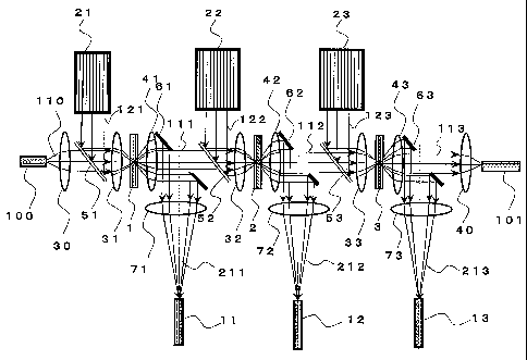
Fig. 1 shows the general configuration of an optical path
switching device according to an Example 1 of the present invention.
41
CA 02497052 2005-02-25
WO 2004/027508 PCT/JP2003/011609
The optical path switching device of Fig. 1 is an example device formed
by serially connecting three sets of optical path switching units
each comprising "a control light source, dichroic mirror, condenser
lens, thermal lens forming element, receiver lens, and mirror having
a hole". In theory, the number of connected optical path switching
units is not limited and may be any number, including one or any greater
number. However, in practice, the possible number of connections is
calculated based on transmittance of signal light in each optical
path switching unit, initial intensity of the incident signal light
introduced into the optical path switching device, and required final
signal light intensity. For example, when transmittance of each unit
is 80%, the resulting total transmittance of a device comprising three
serially connected units is 510.
The optical path switching device of Fig. 1 comprising three
serially connected units will next be explained in detail as one example .
Figs . 2A, 2B, 3A, and 3B are partial views showing the condenser lens
31 and the thermal lens forming element 1 of Fig. 1. Figs. 4A and
4B are partial views further showing the receiver lens 41 and the
mirror 61 having a hole, addition to the components shown in Figs.
2A-3B. Although in all of the above-referenced Figs. 1-4B the thermal
lens forming element 1 is illustrated as having a three-layer structure
comprising a "heat transmission layer film 91 / light absorption layer
film 92 / heat transmission layer film 93" structure, the thermal
lens forming element 1 not limited to such a structure.
An incident signal light 110 output from an optical fiber 100
is adjusted using a collimator lens 30 such that the signal light
110 becomes a substantially parallel beam having a beam radius of
42
CA 02497052 2005-02-25
WO 2004/027508 PCT/JP2003/011609
5.Omm. In the present example, a semiconductor laser having an
oscillation wavelength of 780nm was used as the signal light source.
A semiconductor laser having an oscillation wavelength of 1350nm or
1550nm may alternatively be used. Further, in the present example,
a semiconductor laser having an oscillation wavelength of 650nm was
used as each of the control light sources 21, 22, and 23 for generating
the control lights 121, 122, and 123 used to form thermal lenses in
the respective thermal lens forming elements 1, 2, and 3. An optical
path of the signal light is switched by turning on and off the control
lights. The control lights 121, 122, and 123 are employed after being
shaped into a substantially parallel beam having a beam radius of
4 . 5mm. Zaser power of each of the control light sources provided before
the respective condenser lenses 31, 32, and 33 is in a range between
2-lOmW.
The control lights 121, 122, and 123 and the signal lights 110,
111, and 112 are converged using common condenser lenses 31, 32, and
33, respectively, and irradiated on the thermal lens forming elements
1, 2, and 3, respectively. The signal and control lights are adjusted
using the dichroic mirrors 51, 52, and 53 such that those signals
become coaxial and parallel to one another, thereby allowing the beam
waists of the signal and control lights to overlap within the thermal
lens forming elements. With this arrangement, thermal effect
generated by light absorption in the beam waist region of the control
light can be efficiently exploited for changing the direction of the
signal light.
When laser light is converged using a lens, the light intensity
distribution at the beam waist (converged point or focus) takes the
43
CA 02497052 2005-02-25
WO 2004/027508 PCT/JP2003/011609
form of a Gaussian distribution. A laser light within a wavelength
band that is absorbed by the light absorption film is used as the
control light. This laser light is irradiated through the condenser
lens onto the thermal lens forming element including a light absorption
film, and converged within the light absorption film layer including
the thermal lens forming layer. As a result, the light absorption
film absorbs the laser light, thereby increasing the temperature and
reducing the refraction index of the thermal lens forming layer. When
a light having a Gaussian distribution as described above is irradiated,
the area of the light absorption film layer which receives the
irradiation of the converged center segment of the Gaussian
distribution having the highest light intensity becomes the "center
oflight absorption". Thiscenter area attainsthe highest temperature
as well as the lowest refraction index. The absorbed light in the
region from the center area of light absorption toward the outward
areas changes into heat. Due to this heat and the further outward
spreading heat, the refraction index of the light absorption film
layer including the thermal lens forming layer changes from the center
of light absorption toward the outward areas in a spherical manner,
generating a distribution of refraction index which is small in the
center of light absorption and increasing toward the outward areas.
This arrangement functions as a concave lens. Zight passes at a higher
speed in an area where refraction index is smaller. Accordingly, the
speed of light passing through the area irradiated by the center segment
of the Gaussian distribution having high light intensity is higher
than the speed of light passing through the areas irradiated by
peripheral segments of the Gaussian distribution having low light
44
CA 02497052 2005-02-25
WO 2004/027508 PCT/JP2003/011609
intensity. Consequently, light bends toward the directions of the
areas irradiated by the peripheral segments of the Gaussian
distribution having low light intensity. This effect is identical
to that of a concave lens generated in atmosphere.
In the present example, the signal lights obtained after passing
them through the thermal lens forming elements 1, 2, and 3 are collimated
into substantially parallel beams using the receiver lenses 41, 42,
and 43. The numerical aperture (NA) of these receiver lenses are
selected to be greater than the NA of the condenser lenses. In the
present example, the condenser lens NA was 0.25, while the receiver
lens NA was 0.55. The receiver lens NA is preferably no less than
double the condenser lens NA. As long as this relationship is satisfied,
combinations of the condenser and receiver lens NAs other than that
of the present example are possible. When the receiver lens NA is
no less than double the condenser lens NA, the receiver lens can receive
light without any loss even when the beam diameter of the signal light
is expanded to double the initial beam diameter of the signal light.
first introduced into the thermal lens forming element. In the present
embodiment, focal distances of the condenser and receiver lenses are
identical, and effective diameter of the condenser lenses are
approximately l0mm.
The signal lights collimated by the receiver lenses 41, 42, and
43 are irradiated on the respective mirrors 61, 62, and 63 having
a hole. As described later in detail, these mirrors with hole allow
switching of the optical paths of the signal lights.
On one hand, as shown in Fig. 2A, a control light having a
wavelength within an absorption band of the light absorption layer
CA 02497052 2005-02-25
WO 2004/027508 PCT/JP2003/011609
film and a signal light having a wavelength within a transmission
band may be simultaneously irradiated so as to be focused in a location
close to the incident surface of the light absorption layer film
of the thermal lens forming element 1. In this case, as shown in Fig.
5 3A, a thermal lens 50 is formed by the control light in the location
close to the incident surface. Because of this thermal lens 50, the
cross-section of the signal light is spread in an annular manner,
and the signal light is output as a dispersed output light 201 having
a spread angle greater than that of a normal output light 200. On
the other hand, as shown in Fig. 2B, the control and signal lights
may be simultaneously irradiated so as to be focused in a location
6 close to the output surface of the light absorption layer film of
the thermal lens forming element. In this case, as shown in Fig. 3B,
a thermal lens 60 is formed by the control light in the location close
to the output surface. Because of this thermal lens 60, the signal
light is output as a converged output light 117. In both cases shown
in Figs . 2A and 2B, when the irradiation of the control light is ceased,
the signal light receives no influence of the thermal lenses 50 or
60, and is output as an output light 200 having a normal spread angle.
To examine the above-described thermallenseffect,measurements
were made to determine differences in light intensity distribution
in the signal light beam cross-section generated in accordance with
the presence of the thermal lens effect and the difference in converging
point location. More specifically, in a device as generally shown
in Fig. 1 or Figs. 4A and 4B having the receiver lens 41 NA of 0.55
and the condenser lens 31 NA of 0.25, a light intensity distribution
measuring device 700 as generally shown in Fig. 7 was provided in
46
CA 02497052 2005-02-25
WO 2004/027508 PCT/JP2003/011609
place of the mirror 61. The entire signal light beam that passed through
the thermal lens forming element 1 was received on the receiver lens
41 for collimating the beam. The parallel beam was then introduced
into a light-receiving section 701 (having an effective diameter of
20mm) of the light intensity distribution measuring device, so as
to measure the light intensity distribution in the signal light beam
cross-section. The measurement results are shown in Figs . 8, 9, and
. In the light intensity distribution measuring device 700, as shown
in Fig. 7, a first slit 702 having a width of 1mm is provided in the
10 light-receivingsection701. In the lengthwise direction of the first
slit, namely, in the direction from point 710 to point 720 in Fig.
7, a second slit 703 having a width of 25um is moved at a constant
speed. Thelightintensity distribution measuring device700measures
the intensity of light passing through the rectangular window of 1mm
x 25um formed by the two slits as the window is moved, thereby providing
measurements corresponding to the movement of the window. When
measuring light intensity corresponding to the moved positions of
the window, outputs from the detecting section which received the
light passing through the window may be, for example, recorded using
a storage oscilloscope in synchronization with the moving speed of
the second slit 703. Each of Figs. 8-10 shows a light intensity
distribution in a beam cross-section of a signal light recorded by
a storage oscilloscope in the above-described manner. In Figs. 8-10,
the coordinate system is defined such that, on the horizontal axis
(indicating position within the beam cross-section), 0 denotes the
center of the light-receiving section 701. Further, the position of
point 710 in Fig. 7 is in the negative direction, while the position
47
CA 02497052 2005-02-25
WO 2004/027508 PCT/JP2003/011609
of point 720 is in the positive direction. The vertical axis indicates
light intensity.
Fig. 8 illustrates a case corresponding to Fig. 4A, showing a
light intensity distribution in a signal light beam cross-section
obtained when no control light but the signal light alone is introduced
into the thermal lens forming element 1. The light intensity
distribution in this case is such that intensity is high in the central
portion but gradually becomes lower toward the peripheral portions
(roughly a "Gaussian distribution"). Accordingly, by positioning a
mirror 61 provided with a hole 161 of a sufficiently large size as
shown in Fig. 4A, the entire signal light beam 111 can pass through
the hole 161 of the mirror 61. Assuming that d1 denotes the beam diameter
of the signal light entering the condenser lens 31 (having focal distance
f1) as a parallel beam, and d2 denotes the beam diameter of the signal
light 111 collimated into a parallel beam by the receiver lens 41
(having focal distance f2), the following equation holds true:
f 1 : f 2=dl : d2 ... [
Accordingly, d~ can be calculated by equation [6].
d2= (f2/fl) ~dl ... [67
In the present Example 1, the mirror 61 is positioned at an angle
of 45 degrees with respect to the optical axis of the signal light.
Further, the cross-section of the signal light passing through the
hole 161 is circular. Therefore, it is necessary that the shape of
the hole 161 is an ellipse having a minor axis D1 and a major axis
D2. The relationship between Dl and D2 can be expressed by the following
equation:
... [7~
48
CA 02497052 2005-02-25
WO 2004/027508 PCT/JP2003/011609
Here, the minor axis Dl of the hole 161 of the mirror 61 should
be greater than the beam diameter d2 of the signal light 111 obtained
by equation [6]. However, if D1 is excessively large, a portion of
a signal light expanded in an annular manner by irradiation of the
control light may undesirably pass through the hole. Accordingly,
the optimal value of D~ is d~ multiplied by a value in the range between
1. 02 and 1. 20, and more preferably in the range between 1. 01 and 1. 10.
In the present Example 1, the focal distance fl of the condenser
lens 31 and the focal distance f~ of the receiver lens 41 were identical .
Therefore, the beam diameter dl of the signal light 110 entering the
condenser lens 31 and the beam diameter d~ of the signal light 111
collimated into a parallel beam by the receiver lens 41 were identical,
being 10mm as noted above. Accordingly, the minor axis D1 of the hole
161 of the mirror 61 is preferably in the range between 10.2mm and
l2.Omm, and more preferably in the range between 10.1mm and ll.Omm.
The actual value of minor axis Dl of Example 1 was 10 . 5mm. From equation
[7], D2 was calculated to be 14.8mm. Furthermore, the mirror used
had a sire (a squarish shape having a side length of 50mm) sufficient
for reflecting a beam having a diameter of 30mm at an angle of 45
degrees.
Fig. 9 shows a light intensity distribution in a signal light
beam cross-section obtained when the focus (converging point) is set
at the location 5 ( on the light incident side ) close to the condenser
lens 31 of the thermal lens forming element 1, and a control light
is irradiated. The light intensity distribution in this case is such
that intensity is low in the central portion and increased in the
peripheral portions in an annular manner. Light intensity in the
49
CA 02497052 2005-02-25
WO 2004/027508 PCT/JP2003/011609
central portion of the signal light beam cross-section is reduced
depending on the control light intensity and the positional
relationship between the thermal lens forming element 1 and the focus.
As the control light intensity is increased, the light intensity in
the central portion of the signal light beam cross-section approaches
zero. The portion having the highest signal light intensity is
located beyond the initial beam diameter ( at a portion around a diameter
of approximately l5mm).
Use of the thermal lens effect corresponding to Fig. 10 is
described referring to an Example 2.
In summary, in the optical arrangement of Fig. 3A, according
to whether or not the control light is irradiated, the light intensity
distribution in the beam cross-section of the signal light after passing
through the thermal lens forming element is switched between the annular
distribution of Fig. 9 (when the control light is irradiated) and
the Gaussian distribution of Fig. 8 (when the control light is not
irradiated) . These two types of light intensity distributions in the
signal light beam cross-section can be discretely extracted using
a mirror having a hole and a shape appropriate for the shapes of the
distributions, thereby accomplishing switching of the signal light
optical path.
In the present Example 1, the mirror 61 is positioned at an angle
of 45 degrees with respect to the optical axis of the signal light.
The mirror surface of the mirror 61 was formed by sputtering or
depositing an aluminum film on a glass surface. The hole 161 of the
mirror 61 was created by boring an elliptical hole in the glass at
a tilt angle of 45 degrees. Instead of creating a hole, it is possible
CA 02497052 2005-02-25
WO 2004/027508 PCT/JP2003/011609
to simply omit attaching the aluminum reflection film in the elliptical
shape. However, it is more preferable to create a hole because a glass
surface reflects several o of an incident light, and this may cause
attenuation and cross-talk of a signal light. The reflection film
is not limited to a film made of aluminum, and may be a film composed
of any material which reflects both the control and signal lights
used, such as, for example, gold and silver.
The signal lights 211, 212, and 213 extracted by changing the
initial signal beam direction by 90 degrees by executing the
above-described optical path switching are converged by condenser
lenses 71, 72, and 73 to be input in optical fibers 11, 12, and 13,
respectively.
When all of the control light sources 21, 22, and 23 are turned
off, the signal light receives no influence of thermal lens effect
and is sequentially output as the signal lights 111, 112, and 113.
The output signal light 113 is converged by a condenser lens 40 to
be input in an optical fiber 101.
It should be noted that the signal light may be input in a detector
or the like, instead of an optical fiber 11, 12, 13, or 101, so as
to convert the carried information into an electric signal for
extraction.
Unless the transmittance of the control light through the thermal
lens forming elements 1, 2, and 3 is Oo, the control light is also
transmitted and output from the thermal lens forming elements 1, 2,
and 3 by an amount corresponding to the transmittance value. In order
to prevent this control light from entering a subsequent thermal lens
forming element to cause erroneous operation or cross-talk, it is
51
CA 02497052 2005-02-25
WO 2004/027508 PCT/JP2003/011609
necessary to minimizeto as close to 0% as possible the transmittance
of the control light through the thermal lens forming elements 1,
2, and 3. Furthermore, it is preferable to provide a wavelength
selection filter (not shown) after each of the thermal lens forming
elements 1, 2, and 3 or the receiver lenses 41, 42, and 43. A desired
known wavelength selection filter can be employed as long as the filter
completely blocks light within the wavelength band of the control
light while efficiently transmitting light within the wavelength band
of the signal light. For example, a plastic or glass colored with
a dye or a glass having a dielectric multilayer deposition film on
its surface may be used as the wavelength selection filter.
Alternatively, it is also possible to form a thin film of a wavelength
selection filter material on the surfaces of the receiver lenses 41,
42, and 43 by a process such as coating or sputtering, thereby allowing
the thin film to serve the function of the wavelength selection filter.
The optical path switching device of the present Example 1 is
formed by serially connecting three sets of optical path switching
units each comprising "a control light source, dichroic mirror,
condenser lens, thermal lens forming element, receiver lens, and mirror
having a hole". According to this arrangement, when all of the control
lights are turned off, the signal light proceeds straight and is input
in the optical fiber 101. In contrast, when the control light 21 is
turned on, the signal light 211 is input in the optical fiber 11.
When the control light 21 is turned off and the control light 22 is
turned on, the signal light 212 is input in the optical fiber 12.
Moreover, when the control lights 21 and 22 are turned off and the
control light 23 is turned on, the signal light 213 is input in the
52
CA 02497052 2005-02-25
WO 2004/027508 PCT/JP2003/011609
optical fiber 13. In this manner, optical paths of the signal light
can be switched.
The thermal lens forming element 1 of Example 1 is illustrated
in Fig. 6 as a thermal lens forming element 600 to show its general
cross-sectional structure. A signal light 608 and a control light
609 are converged by a condenser lens 610 and irradiated on the thermal
lens forming element 600. The rays of the control light 609 are
schematically illustrated without showing refractions generated
between the layer films.
The thermal lens forming element 600 having a "heat conduction
layer film 601 / light absorption film 603 / thermal lens forming
layer 605 / light absorption film 604 / heat conduction layer film
602" structure can be produced through the following process.
A vacuum container for cleaning substrates was connected via
a gate valve to a vacuum vapor deposition device . Inside the vacuum
container, two ultraviolet lamps each having a center wavelength of
185nm and an output of 5W and two ultraviolet lamps each having a
center wavelength of 254nm and an output of 5W were installed in
positions allowing ultraviolet light to be irradiated on a substrate
surface. One or more glass plates (24mm x 30mm x 0.15mm) were placed
in the vacuum container as the substrate ( serving as the heat conduction
layer films 601 and 602) . Subsequently, at the atmospheric pressure,
the vacuum container was filled with clean nitrogen gas obtained by
passing nitrogen gas through a gas filter rated to trap 100 0 of particles
having a diameter of 0.05um or more. This process for purifying the
atmosphere inside the vacuum container was continued until floating
particles (of diameter 0.lum or larger) and contaminating gases were
53
CA 02497052 2005-02-25
WO 2004/027508 PCT/JP2003/011609
no longer detected. Next, oxygen gas obtained after passing oxygen
gas through a gas filter rated to trap 100 o a particles having a diameter
of 0.05um or greater was introduced into the vacuum container until
the oxygen concentration became 600 or higher. The ultraviolet lamps
were then turned on to perform ultraviolet irradiation treatment and
ozone treatment of the substrate surface for one hour. After completing
the above-described cleaning process, the inside of the vacuum
container for cleaning substrates was evacuated to attain a high-vacuum
state of 10-4Pa or lower. Subsequently, the substrate was transferred
to the vacuum vapor deposition device similarly in a high-vacuum state
of 10-4Pa or lower. Platinum phthalocyanine (composition formula:
Cs2Hi6NaPt) , which was introduced in advance in the deposition source,
was heated with a resistance wire to 600°C so as to be vacuum-deposited
on the substrate. During this process, the substrate temperature was
not controlled. Progress of the deposition was monitored using a quartz
resonator type film thickness meter. When the film thickness reached
0.2um, a shutter of the deposition source was closed to end the
deposition process.
The surface of the deposition film formed on the substrate by
the above procedures wasphotographed by scanning electron microscope
photography. From the photographs, it was observed that the platinum
phthalocyanine that was vacuum-deposited under the above-described
conditions existed in a state of particles having outer diameters
in a range of between 30 and 50nm. Such a particle diameter size is
smaller than 1/10 of the signal light wavelength ( 780nm) and the control
light wavelength (633nm)employedin the present Examplel. Particles
of this size would not cause light scattering.
54
CA 02497052 2005-02-25
WO 2004/027508 PCT/JP2003/011609
In the meantime, a solution obtained by dissolving 1g of
polycarbonate resin (Panlite 21250 (registered trademark)
manufactured by Teijin Chemicals Ztd.) into 19g of dichloromethane
was poured into 300m1 of n-hexane while mixing. The deposited resin
clusters were filtered, then cleansed with 30m1 of n-hexane.
Subsequently, the solvent was removed in a clean atmosphere. The
clusters were grinded so as to obtain a fine powder having a particle
diameter of less than 50um. The obtained polycarbonate resin fine
powder was deaired by gradually heating to a temperature range between
100-120°C for 48 hours inside a high-vacuum container of 10-4Pa or
lower.
Also in a clean atmosphere, the resin fine powder after
high-vacuum de-airing was sprayed on the platinum phthalocyanine
deposition film formed on a glass substrate according to the above
procedures. Another platinum phthalocyanine deposition film formed
on a glass substrate was placed thereon. This multilayer material
was then placed on a heating stage inside a high-vacuum container.
The inside of the container was evacuated to 10-4Pa or lower, and heated
to 240-260°C. In addition, pressurizing plates heated to 240-
260°C
were used to compress the multilayer material, thereby performing
vacuum hot pressing under a pressure of 5kgf/cm2.
A multilayer thermal lens forming element having the structure
comprising "glass (heat conduction layer film 601 having a thickness
of 150pm) /platinum phthalocyanine deposition film(light absorption
film 603; 0.2um) / polycarbonate resin layer (thermal lens forming
layer 605; 20um) / platinum phthalocyanine deposition film (light
absorption film 604; 0.2um) / glass , (heat conduction layer film 602;
CA 02497052 2005-02-25
WO 2004/027508 PCT/JP2003/011609
150~am) " was produced using the process described above . Transmittance
of the thermal lens forming element was 81% for the signal light having
a wavelength of 780nm, and 0 . 09 0 (substantially 0 0 ) for the control
light having a wavelength of 633nm.
The thickness of the thermal lens forming layer was controlled
by adjusting the amount of the sprayed resin powder, the heating
temperature, and the pressurizing time (between several minutes to
several hours).
In order to measure the optical response speed of the optical
path switching device of the present Example 1, a continuous light
was used as the signal light, while an intermittent beam having a
rectangular waveform with a frequency in the range between several
Hz to 100Hz and a duty ratio of 1:1 was employed as the control light.
These signal and control lights were irradiated so as tomake comparisons
of the magnitudes of intensity amplitudes of the signal lights obtained
via optical path switching.
Each of Figs. 13 and 14 shows a waveform 1210 of the control
light 121 output from the control light source 21 in Fig. 1 measured
using an oscilloscope by introducing the control light 121 into an
optical detector, and a waveform 2110 of the switched signal light
211 measured using an oscilloscope by introducing into an optical
detector the signal light 211 having its optical path switched in
accordance with the ON/OFF of the control light 121. It is to be noted
that the scale of the vertical axis of Fig. 14 is thrice that of the
vertical axis of Fig. 13. Further, Fig. 15 shows the measurements
of amplitude L of the signal light waveforms 2110 generated in accordance
with the signal light intermittency resulting when the frequency of
56
CA 02497052 2005-02-25
WO 2004/027508 PCT/JP2003/011609
the rectangular waveform of the intermittent control light 121 was
set within the range between 200Hz and 100kHz.
As shown in Fig. 13, the rectangular waveform of the intermittent
control light 121 (Fig. 1) has a frequency of 500Hz. Assuming that
the amplitude L of the signal light waveform 2110 generated in accordance
with the signal light intermittency resulting in this case is the
reference amplitude value of 1, amplitude L of approximately 1 was
obtained when the frequency of the rectangular waveform of the
intermittent control light 121 was set within the range between 0 . 2-2 kHz .
In other words, it was confirmed that optical path switching can be
completed in 500 microseconds . This response speed is more than twice
that of an optical switch using a thermooptical effect employing an
electric heater, which has a response speed on the order of milliseconds .
As an example in which a control light having a higher frequency
is used, Fig. 14 shows the signal light waveform 2110 obtained when
the frequency was set at 20kHz. As can be understood from Fig. 14,
when the control light is turned off before complete optical path
switching is executed by the thermal lens effect, the obtained signal
light has a sawtooth waveform, and the amplitude L is reduced. In
other words, when the frequency exceeds the response speed of the
thermal lens effect, optical path switching becomes incomplete, such
that a portion of the signal light remains proceeding straight without
its path being switched.
In order to measure the durability of the optical path switching
device of the present Example 1, a continuous light was used as the
signal light, while an intermittent beam having a rectangular waveform
with a frequency of lkHz and a duty ratio of 1:1 was employed as the
57
CA 02497052 2005-02-25
WO 2004/027508 PCT/JP2003/011609
control light. These signal and control lights were irradiated so
as to compare, over time, the magnitudes of intensity amplitudes of
the signal light obtained via optical path switching. No attenuation
was observed in the intensity amplitudes of the signal light even
after continuous 10,000 hours.
In order to test the polarization dependency of the optical path
switching device of the present Example 1, experiments were performed
by inserting one polarization element in each of the signal and control
light beams to vary the polarization angle. However, absolutely no
polarization dependency was detected.
[Example 2]
Fig. 10 shows an example light intensity distribution in a signal
light beam cross-section obtained in an optical arrangement
corresponding to Figs . 3B and 11B, in which a control light is irradiated
while the focus (converging point) is located, as in Fig. 2B, at a
position 6 (on the light output side) close to the receiver lens 41
of the thermal lens forming element 1. In this example, light intensity
in the center portion is greater than the center portion light intensity
obtained when the control light is not irradiated (Fig. 8). While
the center portion light intensity in the signal light beam
cross-section in this example also depends on the control light
intensity and the positional relationship between the thermal lens
forming element 1 and the focus 6, the center portion intensity becomes
several times greater with the control light than when the control
light is not irradiated.
Accordingly, when a mirror 61 is provided in this example, most
58
CA 02497052 2005-02-25
WO 2004/027508 PCT/JP2003/011609
of the signal light beam passes through the hole 161 of the mirror
61. If the size of the hole 161 of the mirror 61 is optimized (to
the diameter of 2mm in the present Example 2 ) , substantially no signal
light is reflected by the mirror 61. On the other hand, even if the
size of the hole 161 of the mirror 61 is optimized, it is impossible
to prevent a central portion of the signal light from passing through
the hole 161 as a signal light leak 116 when the control light is
not irradiated ( as in Figs . 4A and 0 ) . In other words, in the optical
path switching device of Example 2, some signal light leak 116
(cross-talk) is inevitably caused as long as the intensity distribution
in the signal light beam cross-section assumes a Gaussian distribution
or similar form.
In other words, it is possible to reduce such signal light leak
to substantially zero by changing the intensity distribution in a
beam cross-section of the incident signal light into the thermal lens
forming element. More specifically, when shaping a signal light 110
output from the optical fiber 100 using a collimator lens 30, the
intensity distribution in the signal light beam cross-section can
be readily adjusted so as to take the form of an annular distribution
corresponding to Fig. 9 by selecting an appropriate lens shape (e.g.,
a conic lens) or configuration (e.g., a combination of convex and
concave lenses). The signal light 110 having such an annular
cross-sectional intensity distribution may be converged using a
condenser lens 31 to the focal position 6 (Fig. 11A) to thereby be
directed through the thermal lens forming element 1, and subsequently
restored into a parallel beam using a receiver lens 41. The
cross-sectionalintensity distribution of thelight beam thusobtained
59
CA 02497052 2005-02-25
WO 2004/027508 PCT/JP2003/011609
takes the form of an "annular" distribution having high intensity
in the peripheral portions and substantially zero intensity in the
center portion, as shown in Fig. 9. In this manner, it is possible
to substantially eliminate signal light leak through the hole 161
when the mirror 61 is provided. When the intensity distribution in
the signal light beam cross-section is "annular" as described above,
by irradiating a control light to temporarily form a thermal lens
60 as shown in Fig. 11B, the signal light beam can be shaped into
a sharp beam and output as a converged output signal light 117 proceeding
straight through the hole 161 of the mirror 61.
To summarize, in an optical arrangement as shown in Fig. 11,
the foci of the control and signal lights may be adjusted to a position
6 close to the output side of the thermal lens forming element, while
the intensity distribution in the signal light beam cross-section
is made annular. In this manner, the optical path of the output signal
light can be changed by 90 degrees from the initial signal beam direction
when the control light is not irradiated, and, when the control light
is irradiated, the signal light can be allowed to proceed straight .
In order to measure the optical response speed of the optical
path switching device of the present Example 2, a continuous light
was used as the signal light, while an intermittent beam having a
rectangular waveform with a frequency in the range between several
Hz to 100Hz and a duty ratio of 1:1 was employed as the control light.
These signal and control lights were irradiated so as to enable
comparisons of the magnitudes of intensity amplitudes of the signal
lightsobtained via optical pathswitching. From the measured results,
assuming that the signal light intensity amplitude at 1Hz is the
CA 02497052 2005-02-25
WO 2004/027508 PCT/JP2003/011609
reference amplitude value, no change in intensity amplitude was
detected up to 2kHz. When the frequency was further increased, the
intensity amplitude gradually attenuated, reaching half the reference
value at lOkHz . In other words, it was confirmed that a complete optical
path switching was possible within 500 microseconds. This response
speed is twice as high compared to that of an optical switch using
a thermooptical effect employing an electric heater.
In order to measure the durability of the optical path switching
device of the present Example 2, a continuous light was used as the
signal light, while an intermittent beam having a rectangular waveform
with a frequency of lkHz and a duty ratio of 1:1 was employed as the
control light. These signal and control lights were irradiated so
as to compare, over time, the magnitudes of intensity amplitudes of
the signal light obtained via optical path switching. In the results,
no attenuation was observed in the intensity amplitudes of the signal
light even after 10,000 continuous hours.
[Example 3]
The angle at which an optical path of the signal light 110 is
switched with respect to its optical axis can be freely changed in
the range between approximately 5-175 degrees by changing the
positioning angle at which the mirror 61 is positioned in Example
1 (45 degrees with respect to the optical axis of the signal light
110 ) , and determining a new shape ( length of the maj or axis with respect
to the minor axis) of the elliptical hole 161 through calculation
using a trigonometric function based on the new positioning angle.
Furthermore, the switching direction of the signal light 110
61
CA 02497052 2005-02-25
WO 2004/027508 PCT/JP2003/011609
path with respect to its optical axis can be freely changed through
a 360 degree range by rotating the position of the mirror 61 while
using the optical axis of the signal light 110 as the rotational axis,
and accordingly adjusting the position of the condenser lens 71 and
the like.
[Example 4]
An optical switching device of Example 4 was assembled in an
identical manner as the device of Example 1, except that a thermal
lens forming element produced according to the following procedures
was used in place of the thermal lens forming element of Example 1
which includes a platinum phthalocyanine deposition film in the light
absorption layer film. By performing the optical switching process
using the device of Example 4, results equivalent or superior to those
of the device of Example 1 could be accomplished.
First, tetraamino copper phthalocyanine was diazotized in
concentrated hydrochloric acid. To the obtained material, a monomer
mixture of methylmethacrylate,butyl methacrylate,and2-hydroxyethyl
methacrylate (at the molar ratio of 4:1:1) was added. The mixture
was then gradually heated to synthesize a polymer-bonded dye containing
copper phthalocyanine (the mass of copper phthalocyanine in the total
mass was approximately 60 0 ) . The dye was dissolved in 2-butanone to
eliminate acids and insoluble substances, and then refined by passing
it through a column using 2-butanone as the solvent. The filler of
the column was alumina (having an average particle diameter of
approximately 50um) that was aerated to reduce its activity.
Subsequently, the refined polymer-bonded dye was mixed with a
62
CA 02497052 2005-02-25
WO 2004/027508 PCT/JP2003/011609
polycarbonate resin in dichloromethane to obtain a mixture containing
the polymer-bonded dye at 0 . 5 o by weight with respect to the resin.
The solvent was then eliminated, and the resulting material was grinded
into fine powder. The powder was deaired by gradually heating from
room temperature to 200°C in a high-vacuum state of 10-4Pa or lower.
A vacuum container for cleaning substrates was connected via
a gate valve to a vacuum vapor deposition device. Inside the vacuum
container, two ultraviolet lamps each having a center wavelength of
185nm and an output of 5V~1 and two ultraviolet lamps each having a
center wavelength of 254nm and an output of 5G~7 were installed in
positions allowing ultraviolet light to be irradiated on a substrate
surface. One or more glass plates (24mm x 30mm x 0.15mm) were placed
in the vacuum container as the substrate ( serving as the heat conduction
layer films 601 and 602 ) . Subsequently, at the atmospheric pressure,
the vacuum container was filled with clean nitrogen gas obtained by
passing nitrogen gas through a gas filter that traps 100 0 of particles
having a diameter of 0.05um or greater. This process for purifying
the atmosphere inside the vacuum container was continued until floating
particles of diameter 0.lum or larger and contaminating gases were
no longer detected. Next, oxygen gas obtained after passing oxygen
gas through a gas filter rated to trap 1000 of particles having a
diameter of 0. 05um or greater was introduced into the vacuum container
until the oxygen concentration became 600 or higher. The ultraviolet
lamps were then turned on to perform ultraviolet irradiation treatment
and ozone treatment of the substrate surface for one hour. After
completing the above-described cleaning process, the inside of the
vacuum container for cleaning substrates was evacuated to attain a
63
CA 02497052 2005-02-25
WO 2004/027508 PCT/JP2003/011609
high-vacuum state of 10-4Pa or lower. Subsequently, the substrate
was transferred to a vacuum hot pressing device similarly in a
high-vacuum state of 10-4Pa or lower.
The powder mixture of the polymer-bonded dye containing copper
phthalocyanineand the polycarbonate resin prepared asdescribed above
was placed between two glass plates having surfaces cleaned as described
above. This multilayer material was subjected to hot pressing at 250°C
in a high-vaouum state of 10-4Pa or lower, then cooled to room
temperature.
By the above-described process, a thermal lens forming element
having the structure comprising "glass (heat conduction layer film
601; 150um) / a layer (25um) simultaneously serving as the light
absorption film and the thermal lens forming layer, composed of a
mixture of a polymer-bonded dye containing copper phthalocyanine and
a polycarbonate / glass (heat conduction layer film 602; 150um) " was
produced.
In order to measure the optical response speed of the optical
path switching device of the present Example 4, a continuous light
was used as the signal light, while an intermittent beam having a
rectangular waveform with a frequency in the range between several
Hz to 100Hz and a duty ratio of 1:1 was employed as the control light.
These signal and control lights were irradiated so as to enable
comparisons of the magnitudes of intensity amplitudes of the signal
lights obtained via optical path switching. In the measured results,
assuming that the signal light intensity amplitude at 1Hz is the
reference amplitude value, no change in intensity amplitude was
detected up to 3kHz. When the frequency was. further increased, the
64
CA 02497052 2005-02-25
WO 2004/027508 PCT/JP2003/011609
intensity amplitude gradually attenuated, reaching half the reference
value at l2kHz. In other words, it was confirmed that optical path
switching can be completed in 333 microseconds . This response speed
is more than three times that of an optical switch using a thermooptical
effect employing an electric heater.
In order to measure the durability of the optical path switching
device of the present Example 4, a continuous light was used as the
signal light, while an intermittent beam having a rectangular waveform
with a frequency of lkHz and a duty ratio of 1:1 was employed as the
control light. These signal and control lights were irradiated so
as to compare, over time, the magnitudes of intensity amplitudes of
the signal light obtained via optical path switching. From the results,
no attenuation was observed in the intensity amplitudes of the signal
light even after 20,000 continuous hours.
INDUSTRIAL APPZICABIZ,ITY
As described above in detail, the present invention provides
an optical path switching device and method in which no electric circuits
or mechanically moving parts are used. Such an optical path switching
device and method are reliable, have excellent durability, and have
no polarization dependency. Further, the optical path switching
angles and directions can be freely set. Other advantages of the
present invention are that attenuation of the signal light intensity
is reduced, and that the device and method can be used in a multi-linked
manner. Moreover, the optical path switching device and method
accomplishes a sufficiently fast practical response speed.
Accordingly, the present invention provides an optical path
CA 02497052 2005-02-25
WO 2004/027508 PCT/JP2003/011609
switching device (optical switch) which does not employ an electric
signal, in other words, an optical-to-optical direct switch, which
is advantageously capable of dealing with the exponential increase
in network traffic resulting from widespread use of the Internet and
intranets in homes and offices.
66