Note: Descriptions are shown in the official language in which they were submitted.
CA 02498993 2005-03-01
HARMONIC MITIGATING DEVICE WITH MAGNETIC SHUNT
FIELD OF INVENTION
This invention relates to harmonic mitigating devices for electrical power
distribution systems. In particular, this invention relates to a solid state
passive
harmonic mitigating device for connection between the power distribution
system and
one or more harmonic-generating loads, to reduce the levels of harmonic
currents
flowing into the power distribution system.
BACKGROUND OF THE INVENTION
Electrical distribution systems, for example for distributing an electrical
power
supply through a building or industrial facility, are often subjected to
harmonic
currents generated by non-linear loads such as electronic equipment (including
computers, adjustable speed drives (ASD), uninterruptable power supplies
(UPS),
power rectifiers, etc.) and equipment that uses different kinds of arc
processes
(including arc discharge lighting systems). These harmonic-generating loads
generate
various levels of conventional harmonics (5th, 7th, 1 Ith, 13th, 17th, 19th,
23rd, 25th
etc.) and, for single phase line-to-neutral non-linear loads, also zero phase
sequence or
"triplen" harmonics (3rd, 9th etc.) in the power distribution system, the
harmonic
spectrum depending upon the nature of the harmonic-generating load.
These harmonic currents create many problems in the power distribution
system, including increased voltage total harmonic distortion level, reduced
electromagnetic compatibility of the loads, reduced reliability of the power
distribution equipment, increased power losses, reduced power factor, and
other
problems which are well known to those skilled in the art.
Prior art systems for mitigating harmonic currents fall into six basic types:
1. Power factor corrected (PFC) power supplies: In these systems the rectified
current is continually adjusted to smooth the current consumption waveform.
PFC's
are relatively expensive devices and their applications are limited. Also,
PFC's cannot
be retrofitted for use with existing power supplies, and are not practical for
use with
large ASD's.
1
CA 02498993 2005-03-01
2. Active filters: These devices inject into the conductors between the power
distribution system and the load, harmonic currents having a polarity opposite
to those
generated by the load, thereby neutralizing harmonic currents flowing into the
power
distribution system. Active filters have many disadvantages, including high
cost, poor
reliability. Active filters also are not practical for use with large ASD's.
3. Resonant L-C filters: L-C filters are commonly used in power systems,
tuned to different harmonic frequencies to mitigate specific harmonic
currents. These
devices present many problems which are well known to those skilled in the
art,
including high cost and the tendency to cause the system to operate with a
leading
power factor. Further, because L-C filters are non-directional they are easily
overloaded by untreated harmonic currents generated by other harmonic sources
connected to the power distribution system (for example in a neighboring
facility),
resulting in overloading and frequent failures of the filter's capacitor bank.
4. AC chokes: In this harmonic mitigating technique reactors are connected in
series between the line and the load. This technique is simple, reliable and
relatively
low cost, however it results in a high voltage drop across the reactors. To
reduce the
voltage drop one must reduce the choke reactance level, which commensurately
reduces the effectiveness of the choke and substantially limits harmonic
current
mitigation.
The voltage can be boosted by connecting a capacitor bank between the load
and the choke, but this frequently causes the system to operate with a leading
power
factor (especially in the case of light loading). In this case, since the
reactance of the
reactor at harmonic frequencies is much higher than the reactance of the
reactor at the
fundamental frequency, a large part of the harmonic currents drain through the
capacitor. The capacitor has a high reactance at the fundamental frequency.
However,
the voltage drop across the choke remains very high. Thus, large compensating
capacitors must be connected between the load and the choke to boost the
voltage,
which substantially increases the size and cost of the system and causes the
system to
operate at increased voltage levels during light loading conditions.
2
CA 02498993 2011-05-31
5. Phase shifting systems: Different kinds of phase shifters are available
which
allow the creation of quasi-multiphase systems, reducing certain harmonic
levels.
Harmonic currents of targeted orders are cancelled or substantially reduced
depending
upon the selected degree of the phase shift. However, such systems are
typically
limited in terms of the number of harmonic orders which can be mitigated, and
the
degree of harmonic mitigation depends upon the extent to which harmonics
produced
by the various harmonic sources are identical.
6. Passive wide-band filters, for example as described in US Patent No.
6,127,743 issued October 3, 2000 to Levin et al., illustrated in Figure 1
herein. This
filter consists of a multiple winding reactor and a capacitor bank. This
filter comprises
a blocking coil (line winding 20 in Fig.1) and filtering component comprising
inductive and capacitive elements in a crosslink circuit. The filter described
and
illustrated in US Patent No. 6,127,743 is effective in eliminating a wide
range of
harmonics from the system.
However, since all inductive elements of the filter in US Patent No. 6,127,743
are wound on a common magnetic core, there is magnetic coupling between the
various inductive elements of the filter. The harmonic currents flowing in the
cross-
link circuit generate a magneto motive force (MMF), and as a result of
magnetic
coupling between the blocking element of the filter (the line winding) and the
cross-
link circuit, the magneto-motive force (MMF) induces harmonic currents in the
blocking element that flow directly into the power supply system, increasing
the total
harmonic current flowing into the power supply system and thereby reducing the
effectiveness of harmonic mitigation by the filter.
Thus, in this solution, as more harmonic currents are diverted by the blocking
element through the cross-link circuit, a greater MMF is generated and a
higher level
of harmonic current is thereby induced in the blocking element. With these
additional
harmonic currents, in order to improve filter performance to the required
level the
impedance level of the blocking element must be substantially increased. This
causes
a substantial voltage boost under no-load conditions, increased voltage drop
at full
load conditions, and sometimes drive stability problems especially when
driving high-
inertia loads. Also, different filter configurations have to be used for 1)
rectifiers
3
CA 02498993 2005-03-01
(drives) with no reactors; 2) rectifiers with DC line reactors; and 3)
rectifiers with
AC line reactors.
The sets of windings could alternatively be wound on separate cores, however
there is a high cost to this both in materials used and in the space occupied
by a
multiple-core device (known as the `footprint').
SUMMARY OF THE INVENTION
The present invention overcomes these disadvantages by providing a harmonic
mitigating device for connection between the power distribution system and the
load,
which allows control over the levels of magnetic coupling between different
elements
of the device while providing all windings on a single core. Control over
magnetic
coupling is accomplished through the use of magnetic shunts. This allows for
the
reduction or elimination of the harmonic MMF induced in the line winding of
the
device, and as a result the reduction of harmonic currents flowing into the
power
supply system. This further allows for the reduction of the line winding
inductance,
which in turn reduces the voltage boost of the device under the no-load
conditions,
reduces the voltage drop at full load conditions and increases the stability
of the drive.
The invention serves to reduce ripple level in rectifier outputs and buffers
transient
overvoltages, and a single configuration works with any rectifier type,
including SCR
bridges.
The present invention thus provides a harmonic mitigating device for
mitigating harmonic currents generated by a load having an input connected to
a
power distribution system and an output connected to the load, comprising a
magnetic
core having three core legs, each corresponding with one of three phases of
the power
distribution system, a magnetic shunt, extending across and magnetically
coupled to
the core legs at an intermediate part thereof, such that first and second
parts of the
core on either side of the shunt, for each phase, a first reactive element
comprising a
line winding having a first end for connection to a first line and a second
end, the line
winding being disposed on the first part of the core, for each phase, a second
reactive
element comprising a first cross-link winding, disposed on the second part and
having
a first end connected to the second end of the line winding and a second end
connected to a capacitor, the capacitor having a second end connected to a
different
4
CA 02498993 2005-03-01
phase or to a capacitor associated with a different phase, whereby the line
winding
and associated cross-link winding for each phase are magnetically coupled by
the
magnetic shunt.
The invention further provides a harmonic mitigating device for mitigating
harmonic currents generated by a load having an input connected to a power
distribution system and an output connected to the load, comprising a magnetic
core
having at least one core leg, the core comprising a first part and a second
part a
magnetic shunt, the first and second parts of the core being disposed on
either side of
the shunt, a first reactive element comprising a line winding having a first
end for
connection to a first line of a power supply and a second end, the line
winding being
disposed on the first part of the core, a second reactive element comprising a
cross-
link winding, disposed on the second part of the core and having a first end
connected
to the second end of the line winding and a second end connected to a
capacitor, the
capacitor having a second end connected to a second line of the power supply,
whereby the line winding and associated cross-link winding are magnetically
coupled
by the magnetic shunt.
The invention further provides a magnetic system, comprising a magnetic core
having at least a first portion and a second portion, the first and second
portions being
separated by a magnetic shunt.
In further embodiments of the invention the core is provided with at least one
non-magnetic gap.
IN THE DRAWINGS
In drawings which illustrate by the way of example only a preferred
embodiment of the invention,
Figure 1 is a circuit diagram of a prior art passive wide-band filter.
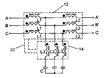
Figure 2 is a first preferred embodiment of three-phase harmonic mitigating
device embodying the invention having in each phase an input winding and a
cross-
link winding on a magnetic core, separated by a magnetic shunt.
5
CA 02498993 2005-03-01
Figure 3 is a schematic diagram of a further preferred three-phase embodiment
of the invention on a magnetic core having in each phase an input winding, an
output
winding and a cross-link winding, with input and output windings disposed on
one
side of a magnetic shunt and the cross-link windings disposed on the other
side of the
magnetic shunt.
Figure 4 is a schematic diagram of a further preferred three-phase embodiment
of the invention on a magnetic core, with input windings disposed on one side
of the
magnetic shunt and the output windings and cross-link windings disposed on the
other
side of the magnetic shunt.
Figure 5 is a schematic diagram of a further preferred three-phase embodiment
of the invention having two windings in each phase of the cross-link circuit,
with the
input windings and one set of cross-link windings disposed on one side of the
magnetic shunt and the output windings and the other set of cross-link
windings
disposed on the other side of the magnetic shunt.
Figure 6 is a schematic diagram of a further preferred three-phase embodiment
of the invention having an output winding and a compensating winding in each
phase
of the output circuit, with the input windings and compensating windings
disposed on
one side of the magnetic shunt and the cross-link windings and output windings
disposed on the other side of the magnetic shunt.
Figures 7 is a schematic diagram of a further preferred three-phase
embodiment of the invention having two windings in each phase of the cross-
link
circuit, with the input windings and one set of cross-link windings disposed
on one
side of the magnetic shunt and the output windings and the other set of cross-
link
windings disposed on the other side of the magnetic shunt, and cross-link
circuits
connected line-to-line.
Figure 8 is a schematic diagram of a further preferred three-phase embodiment
of the invention having one winding in each phase of the cross-link circuit,
with the
input windings and one set of cross-link windings disposed on one side of the
magnetic shunt and the output windings and the other set of cross-link
windings
6
CA 02498993 2011-05-31
disposed on the other side of the magnetic shunt, and cross-link circuits
connected
line-to-line.
Figure 9 is a schematic diagram of a core for the invention having a magnetic
shunt between the input and the output sections of the core, with two windings
in each
section.
Figure 10 is a schematic diagram of a core for the invention having the bottom
yoke of one of the input and output sections of the core serving as a magnetic
shunt
between the input and the output sections, with two windings in each section.
Figure 11 is a schematic diagram of a core for the invention having the top
yoke of one of the input and output sections of the core serving as a magnetic
shunt
between the input and the output sections, with two windings in each section.
Figure 12 is a schematic diagram of a core for the invention with multiple non-
magnetic gaps at the yoke and shunt connections.
Figure 13 is a schematic diagram of a core for the invention with multiple non-
magnetic gaps, including distributed air gaps.
DETAILED DESCRIPTION OF THE :INVENTION
The harmonic mitigating system of the invention may utilized in a multi-
winding reactor having a capacitor bank, similar to that described and
illustrated in
US Patent No. 6,127,743 issued October 3, 2000 to Levin et al., illustrated in
Figure
1. In the embodiments of the invention illustrated and described hereafter,
the power
distribution system 2 may be any AC electrical power source, typically a mains
power
supply powered by an electrical utility or a local generator. The load 4
typically
includes one or more harmonic generating (non-linear) loads, the most common
being
non-linear loads such as adjustable speed drives, rectifiers etc. The harmonic
spectrum of different types non-linear loads may vary, however the device of
the
invention is suitable for mitigating harmonic currents generated by many
different
kinds of harmonic generating loads.
In the prior art harmonic mitigating system 6 illustrated in Figure 1,
described
in US Patent No. 6,127,743, harmonic currents generated by the load 4 are
mitigated
7
CA 02498993 2005-03-01
by interposing reactive elements in the three phases of the power distribution
system
between the power distribution system 2 and the load 4, to establish a
fundamental
current path between the load and the power distribution system 2. The cross-
link
circuit, comprising a three phase capacitor bank, may be connected in Delta
or/and
Wye configurations and connected between the phases to establish low reactance
path
for harmonic currents generated by the load 4. Harmonic currents, which
according to
fundamental electrical principals will primarily follow the path of lowest
reactance,
are thus largely diverted from the power distribution system 2 through the
cross-link
circuit and do not penetrate into the power distribution system 2.
The harmonic mitigation device of the invention improves harmonic
mitigation in a system such as that illustrated in Figure 1 by controlling the
extent of
magnetic coupling between the cross-link windings L3, through which harmonic
currents are diverted from the power system, and the line windings L I.
A first preferred embodiment of the invention, having inputs A, B and C for
connection to the power supply (not shown) and outputs A', B' and C' for
connection
to the load (not shown), is illustrated in Figure 2. According to the
preferred
embodiment, control over the extent of magnetic coupling between the cross-
link
windings L3 and the line windings Ll is accomplished by providing for each
phase at
least one line winding, for example an input winding L1, disposed on first
part 12 of a
magnetic core 10, and at least one cross-link winding L3 disposed on an second
part
14 of a magnetic core 10, the first part 12 and second part 14 being separated
from
one another by a magnetic shunt 20 (the parts 12, 14 of the core 10 and the
shunt 20
are shown in dashed lines). The polarity of the windings L1, L3 induces
magnetic
fluxes that may add (if in the same direction) or partially cancel (if in
opposite
directions) in the magnetic shunt 20.
In the preferred embodiments of the invention the magnetic core is formed
from two magnetic parts 12, 14 separated by the magnetic shunt 20 (see for
example
Figures 9 to 13), although the core 10 may have more than two parts 12, 14 and
more
than one shunt 20 and the principles of the invention will apply equally. The
magnetic
shunt 20 may be viewed as a shared yoke, which conducts magnetic flux
generated by
the windings on either side of the shunt 20 and, by arranging the windings in
a
8
CA 02498993 2011-05-31
selected relative polarity, to partly or fully cancel the opposing magnetic
fluxes in the
magnetic shunt 20.
The ferrous core 10 should preferably be provided with at least one non-
magnetic gap 24, since the magnetic characteristics of ferrous materials are
nonlinear
and vary widely with the load current. With a completely solid ferrous core it
would
be virtually impossible to control the reactance characteristics of the core
10, because
reactance would change drastically as the load current changes. The non-
magnetic gap
24 magnetically decouples the output winding L2 and the cross-link winding U.
The
optimal gap size changes depending upon the rating of the device, influenced
primarily by the cross-section of the core and the number of turns of the
windings.
The gap 24 also allows for large levels of power flow to be conducted through
the
reactor. The non-magnetic gaps may be air gaps obtained by physically
separating the
parts of the core 10, or may be formed from any suitable non-magnetic material
interposed between parts of the core 10.
The desired inductances and separation between the parts 12, 14 of the
magnetic core 10 are achieved by appropriate selection of the non-magnetic
gaps 24,
in terms of both number and size. Each part of the magnetic core 10 should
preferably
be provided with at least one non-magnetic gap 24 in each core leg l Oa, I Ob,
I Oc. The
optimal gap size and quantity of the gaps 24 changes depended upon rating of
the
device. For example, in a reactor for a 600 horsepower, 480 Volt drive the
part of the
core 10 containing the cross-link circuits should have four non-magnetic gaps
24 of
0.159" (4.0 mm) each, while the part of the core 10 containing the line
windings Ll
(and optionally L3, L4) should have five non-magnetic gaps 24 of 0.095"
(2.4mm)
each. The optimum gap number and size can be obtained through experimentation
and/or computer modeling.
A further preferred embodiment of the invention illustrated in Figure 3 has an
output winding L2 connected in series with the input winding L 1 and disposed
on the
same part (first part 12) of the core 10 as the input winding L1. The L2
winding of the
invention may have the same or opposite polarity as the L i winding. The cross-
link
winding L3 is disposed on the other side of the shunt 20, on the second part
14 of the
9
CA 02498993 2005-03-01
core 10, and its polarity is opposite the combined polarities (i.e. direction
of the net
flux) of the line windings LI, L2. The flux separation between the second part
14 and
the first part 12 of the core 10 substantially eliminates the harmonic MMF
generated
in the first part 12 of the reactor by windings LI and U.
Optimization of the harmonic mitigating performance of the invented device
with the other parameters such as the device desired output voltage boost at
no-load
conditions, desired output voltage drop at full load conditions, system
operation
stability etc., can be achieved by computer modeling and/or experimentation to
determine the optimal inductances of windings L1, L2 and L3 and the
capacitance of
the capacitor bank C. Depending on the device configuration, the computer
modeling
should include coupling coefficients or mutual inductances between different
windings.
Many variations of the harmonic mitigating system are available using the
principles of the invention. Figure 4 illustrates an embodiment of the
invention with
input windings LI disposed on the first part 12 of the core 10 and output
windings L2
and cross-link windings L3 disposed on the second part 14 of the core 10.
Figure 5
illustrates an embodiment having two windings L3, L4 in each phase of the
cross-link
circuit, with the input windings LI and one set of cross-link windings L3
disposed on
the first part 12 of the core 10 and the output windings L2 and the other set
of cross-
link windings L4 disposed on the second part 14 of the core 10. Figure 6
illustrates an
embodiment of the invention having a compensating winding L5 in each phase of
the
output circuit, with the input windings L1 and compensating windings L5
disposed on
the first part 12 of the core 10 and the cross-link windings L3 and output
windings L2
disposed on the second part 14 of the core 10. In each case the polarities of
the
various windings are selected so that the net flux generated by the windings
on one
side of the magnetic shunt 20 (e.g. the first part 12 of the core 10) is in a
direction
opposite to the net flux generated by the windings on the other side of the
shunt 20
(e.g. the second part 14 of the core 10).
Complete cancellation of harmonic currents generated by the line windings L1
and cross-link windings L3 is not possible, because these windings although
CA 02498993 2005-03-01
magnetically coupled to the shunt are out of phase. However, substantial
cancellation
is possible with the selection of optimal winding characteristics and
polarities.
Figures 7 and 8 illustrate embodiments of the invention in which the
capacitors in the capacitor bank C of the cross-link circuit are connected
line-to-line
between the cross-link windings and the corresponding phases at the junction
point
between the input windings L1 and output windings L2, creating a parallel
cross-link
circuit for each phase between the input windings LI and output windings L2.
As shown in Figures 9 to 13, there are many possible configurations of a core
according to the invention. In Figure 9 a separate magnetic element forms the
10 shunt 20, disposed between two "E" magnetic elements forming the first and
second
parts 12, 14 of the core 10. In Figure 10 the two "E" magnetic elements
forming the
first and second parts 12, 14 of the core 10 are disposed in the same
direction, the
yoke of the first part 12 forming the shunt 20 while a separate magnetic
element
serves as a yoke to magnetically couple the core legs at the open side of the
"E"
element (shown at the top of Figure 10). In Figure 11 the two "E" magnetic
elements
forming the first and second parts 12, 14 of the core 10 are disposed in the
same
direction, the yoke of the second part 14 forming the shunt 20 while a
separate
magnetic element serves as a yoke to magnetically couple the core legs at the
open
side of the "E" element (shown at the bottom of Figure 11). In each case it is
preferable to provide non-magnetic gaps 24 (for example air gaps) between the
shunt
20 and one of the parts 12, 14 of the core.
In Figure 12 the first and second parts 12, 14 of the core 10 are formed from
separate magnetic leg and yoke elements, and the shunt 20 is a separate
magnetic
element, with non-magnetic gaps 26 provided between elements. Figure 13 shows
an
embodiment like Figure 12, formed from separate magnetic leg and yoke elements
with a shunt 20 also as a separate magnetic element, but with non-magnetic
gaps 26
provided not only between elements, but also "distributed air gaps" at
intermediate
positions along the core legs.
11
CA 02498993 2005-03-01
Although the invention has been described in the context of a three-phase
harmonic mitigating device, the principles of the invention apply also to a
single
phase harmonic mitigating device.
Various embodiments of the invention having been thus described by way of
example only, it will be apparent to those skilled in the art that variations
and
adaptations may be made without departing from the scope of invention, as set
out in
the appended claims.
12