Note: Descriptions are shown in the official language in which they were submitted.
CA 02499091 2012-08-03
1
METHOD FOR TRANSMITTING OPTICAL POLARIZATION MULTIPLEX SIGNALS
The invention relates to a method for transmitting optical
polarization multiplex signals.
Bit rates of 10 Gbit/s per channel are customary today for optical
wavelength multiplex systems. Forty-Gbit/s systems have also been
developed and implemented as models, but these systems are very
demanding in terms of expenditure. Particular problems give rise
therein to distortions in the transmitted signals such as
polarization mode dispersion (PMD) and chromatic dispersion.
Polarization controllers and optical compensation evices ar eused to
compensate said distortions.
Numerous modulation and encoding methods are known from the
communications field and numerous possibilities have been
investigated to find suitable methods leading to a significant
improvement in the transmission characteristics of optical systems.
In the reference entitled "Co-channel Operation Even during extreme
depolarization", authored by Lanki et al. (Telcom Report issued by
Siemens AG, Division Transmission Systems, Issue 1 1988), a radio
relay system is described that transmits orthogonally polarized
signals by means of suitable antennas. Imperfect technical
equipment such as poorly oriented antennas as well as reflections
give rise to cross-polarization faults where one signal overlaps
another actually orthogonal signal in a disruptive manner. The
polarized signals are split at the receiving end by separate
antennas. Adaptive time-domain equalizers are provided for
eliminating cross-polarization faults. The basic concept of
depolarization compensation is to obtain a compensation signal and
add it to the respective main signal. No frequency errors must
occur and any inter-signal time displacements must be compensated.
The change in polarization occurring in a radio relay system is,
however, slight compared to optical transmission over fibers. Any
polarization can occur here.
CA 02499091 2012-08-03
2
An arrangement and a method for transmitting polarization multiplex
signals are described in the publication of an unexamined
application reference DE 101 56 244 Al. A differential phase
modulation is applied at the transmitting end between the
orthogonally polarized transmission signals. Said modulation serves
to control a common polarization transformer, or to control separate
polarization transformers for each transmission channel, by
evaluating interferences. The purpose thereof is to maximize the
control rate with a minimal expenditure requirement. The
polarization transformer can be embodied for compensating
polarization mode dispersion in the optical domain. The
transmission link is for this purpose simulated with the aid of a
double-refracting crystal and employing numerous control voltages as
being "inverse", so that the pulse mode dispersion is compensated.
The measures taken at the transmitting end are frequently
undersirable for reasons of transparency; moreover, both fast and
reliable PMD controlling in the optical range remains demanding in
terms of expenditure.
The object of the invention is to achieve an increase in
transmission capacity during optical data transmission, with said
increase being unattended by increased bandwidth requirements for
optical and electrical system components, and also to further reduce
the expenditure requirements.
Accordingly, in one aspect there is provided a method for
transmitting optical polarization multiplex signals wherein at least
a fist binary signal is converted into a first optical signal and
at least a second binary signal is converted into a second optical
signal polarized orthogonally thereto and the orthogonally polarized
optical signals are then combined into a polarization multiplex
signal and thereupon transmitted, wherein the polarization multiplex
signal is divided at the receiving end into two orthogonally
polarized signal parts in that each polarized signal part is
CA 02499091 2012-08-03
2a
converted in a linear manner into a complex signal, the complex
signals are routed to a multidimensional filter whose coefficients
are controlled in such a way that signals which have been
reconstructed independently of the polarization of the received
polarization multiplex signal and which correspond to the optical
signals are fed out at the filter outputs, and the reconstructed
signals are demodulated and converted into binary signals at the
receiving end.
The combining of four-stage multiphase modulation and polarization
multiplex transmission while employing the same bandwidth and an in-
significantly increased signal-to-noise ratio in particular enables
the data rate to be quadrupled. Two mutually orthogonally polarized
multiphase signals are transmitted, as a result of which minimal
cross-influencing is ensured. Mutual influencing is further
minimized through synchronous transmission of the orthogonal
multiphase signals. Sensitivity to PMD and chromatic dispersion
remains the same with respect to known systems having a lower data
rate, or it increases only slightly.
The compensating of disruptive effects is here subject practically
to the requirements of a conventional system having a quarter the
data rate.
The use of a four-stage differential phase modulation has proved to
be especially advantageous. Complex coherent demodulation is not
necessary here.
The system can of course also be used to transmit a multiplicity of
data signals at a lower data rate in parallel. Synchronous
transmission is advantageous when the data rates are the same since
the polarization signals will influence each other least.
CA 02499091 2005-03-15
2002P11754W0US
PCT/EP03/08997
3
A major advantage of the invention ensues from a specific embodiment
of the method at the receiving end or, as the case may be, of the
receiver. There is no further need here for a polarization control-
ler. A major constituent of the receiver is now a multidimensional
filter rendering the polarization controller superfluous and addi-
tionally enabling compensation of the signal distortions.
In the case of a multidimensional electrical filter the orthogonally
polarized signal parts have to be converted into complex electrical
signals in a linear manner. PMD and chromatic dispersion can thus
likewise be compensated at the electrical level.
No coherent demodulation is necessary when differential multiphase
modulation is employed. An advantageous embodiment of the demodula-
tors enables data bits to be fed out in parallel.
Major parts of the receiver, including the multidimensional filter
and the demodulators, can be embodied digitally depending on the
available circuit technology.
A control for determining the filter coefficients is already embod-
ied digitally.
Exemplary embodiments of the invention are explained in more detail
with the aid of figures.
Figure 1 shows the transmitting part of a transmission system for
implementing the invention,
Figure 2 shows a receiving part according to the invention,
Figure 4 is a circuit schematic of an optoelectric converter,
Figure 5 is a circuit schematic of a complex filter for elucidat-
ing the functioning mode,
CA 02499091 2005-03-15
2002P11754W0US
PCT/EP03/08997
4
Figure 7 is a circuit schematic of a demodulator,
Figure 8 is a diagram for elucidating the functioning mode,
Figure 9 is a circuit schematic of a demodulator that processes
signal components,
Figure 10 shows a first arrangement for determining the filter co-
efficients,
Figure 11 shows a second arrangement for determining the filter
coefficients, and
Figure 12 shows an extensively digitized receiving part.
Figure 1 shows an exemplary embodiment of the transmitting part of a
transmission system for implementing the method according to the in-
vention.
A data signal DS is converted in a serial-to-parallel converter 1
into four parallel binary signals A, B, C, and D. Four synchronous
data streams can also be transmitted. In each case two data streams
A, B and C, D are routed to a DQPSK (Differential Quadrature Phase-
Shift Keying) precoder 2 or, as the case may be, 3. Said precoder
takes account of the preceding and current bit pair and converts the
differences between said bit pairs into four possible phase changes
of 0, 90, 180, and 270 . The modulators 4 and 5 only indicate possi-
ble exemplary embodiments. Its top branch, which generates a phase
angle of 0 or 180 , and the bottom branch, with which a phase angle
of 90 or 270 is set, are activated in each modulator for generating
a multiphase signal (QDPSK signal) E. This results in phase angles
of 450, 135 , 225 , and 315 . An analogous procedure is applied to
the data streams C and D, which are converted in the bottom modula-
tor 5 into the QDPSK signal F. Two polarization controllers 7 and 8
ensure that an output signal QPS1 of a modulator 4 is polarized (at
least approximately) orthogonally to the output signal QPS2 of the
other modulator 5. The thus polarized multiphase signals QPS1 and
QPS2 are combined in a polarization beam combiner 9 into a polariza-
tion multiplex signal PMS, which is transmitted over a transmission
fiber 10.
CA 02499091 2005-03-15
. .
2002P11754W0US
PCT/EP03/08997
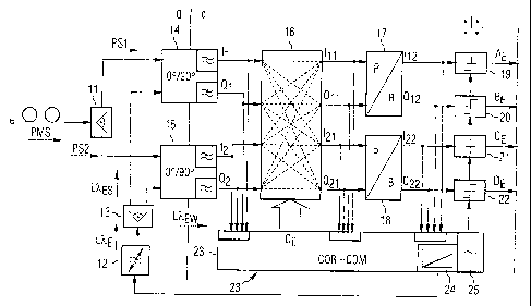
Figure 2 is the circuit schematic of a receiving part for implement-
ing the method according to the invention.
5 The basic functioning of the entire receiving part will first be
briefly described below. The individual elements will then, where
necessary, be described in more detail.
The received polarization multiplex signal PMS is routed to a po-
larization divider 11 which divides it into two orthogonally polar-
ized signal parts PS1 and PS2. The first polarized signal part PS1
is routed to a first optoelectric converter 14; the second polarized
signal part PS2 is routed to an identically designed second opto-
electric converter 15.
The polarized signal parts PS1 and PS2 are each converted into or-
thogonal components II., Ql or, as the case may be, 12, 02 and routed
to a multidimensional filter 16. Said filter recombines portions of
the polarized components into reconstructed signals Iii + jQii or, as
the case may be, 121 + jQ21 corresponding to the optical signals QPS1;
QPS2. The reconstructed signals Ill + jQI1 or, as the case may be, 121
+ jC221 are demodulated in the demodulators 17 and 18 using their or-
thogonal signal components In, Q11 or, as the case may be, In, 021
and converted back in decision stages 19 - 22 into binary signals
AE, BE, CE, and DE at the receiving end. A control 23 controls the
filter 16 and the generation of the clock signals required at the
receiving end.
No polarization controller is provided according to Figure 2 for di-
viding the received polarization multiplex signal PMS. However, as a
consequence of this the polarization at the input of the polariza-
tion divider 11 is of any kind, and the first polarized signal part
PS1 will only tally with the first multiphase signal QPS1 in a very
rare special instance in which the second polarized signal part PS2
also tallies with the second multiphase signal QPS2. Signal parts
_
_______________________________________________________________________________
___________
CA 02499091 2005-03-15
=
2002P11754W0US
PCT/EP03/08997
6
PS1 and P32 will mostly contain portions of both multiphase signals
QPS1 and QPS2, which will then be routed to both the top optoelec-
tric converter 14 and the bottom optoelectric converter 15.
Optical or electrical signals can as a basic rule be processed at
the receiving end. Digitizing and digital processing is likewise
also possible downstream of the converters.
In its left-hand section, the diagram in Figure 3 shows signals at
the input and outputs of the polarization divider 11. The polariza-
tion planes are designated s, standing in German for vertical, and
w, standing in German for horizontal. When polarization is of any
kind, the polarization multiplex signal PMS is applied with its two
orthogonally polarized multiphase signals QPS1 and QPS2 to the input
of the polarization divider. Each signal QPS1 and QPS2 is divided by
the polarization divider 11 in each case into a first "vertical"
signal portion PS11 and into a second "horizontal" signal portion
QS11 or, as the case may be, PS12 and QS12. The vertical components
form the polarized signal part PS1 and the horizontal components
form the polarized signal part PS2. Each signal part therefore con-
tains portions of both multiphase signals QPS1 and QPS2. The "verti-
cally" polarized signal part PS1 is applied to the input of the top
optoelectric converter 14 and the "horizontally" polarized signal
part PS2 is applied to the input of the bottom optoelectric con-
verter 15 (Figure 2).
The basic function of said optoelectric (o/e) converter is to con-
vert the polarized partial signals linearly into a complex electri-
cal signal. The implemented converters each feed out two orthogonal
components I and Ql or, as the case may be, 12 and Q2 (Q: imaginary
part for a complex representation). The orthogonal components can be
further processed more simply. The "complex" output signal I + j(21
of the optoelectric converter 14 is shown in the right-hand section
of Figure 3 (r = real, j = imaginary axis).
CA 02499091 2005-03-15
2002P11,754WOUS
PCT/EP03/08997
7
A transformation to the baseband of the carrier-modulating signal
takes place to practical advantage at the same time as conversion to
an electrical signal. Expressed another way: The optical signal is
transformed linearly from the optical range into the complex base-
band level; immediately ensuing electrical signal processing is then
equivalent to a processing of the optical signal. A signal LXE of a
carrier-frequency generator (laser) at the receiving end is employed
for conversion.
Figure 4 shows an instance of an optoelectric converter 14, 15.
Apart from the polarized signal part PS1 or, as the case may be,
PS2, a similarly polarized carrier-frequency signal LXEs or, as the
case may be, LXEw from the receiving end having in this exemplary em-
bodiment at least approximately the frequency of the carrier signal
1,20 is routed to each converter for optoelectric conversion. Each
converter contains splitters 35, 36 for splitting the input signals,
a phase-shifting element 26, two adders 27, 28, photodiodes 29, 30,
and low passes 31, 32.
If one considers the top converter 14, the polarized signal part PS1
is routed as the input signal to both adders 27 and 28 via the
splitter. The laser signal LXEs is likewise split into two partial
signals, with one part thereof being added in the first adder 27 di-
rectly to the signal PS1. In contrast to this, a signal LXEE90 phase-
shifted by 90 is added in the second adder 28. The summation sig-
nals are each converted by the photodiodes into electrical signals,
corresponding to a squaring according to formula (1):
(1) (Si + LXEO2 = S + 2S1 x LXcs + (L,X,$)2
The signals Si and LX0Es or, as the case may be, LXEs90 are given in
their general form in the equations
(2) Si = A(t)sincoot + cp,,(t)) and
CA 02499091 2005-03-15
2002P11754WOUS
PCT/EP03/08997
8
(3) = B(t)sin(wEt + (19,s(t)) or, as the case may be,
(4)
LAES90 = B(t)sin( E9Ot + 9E590( t))
(5) (S1 + L2\ES90 S + 2S1 x LAES9O + (LAE,90)2.
The first and the last term of the factored out sum according to
formula 1 contain high-frequency oscillations that are removed by
the low pass. The middle term contains a signal portion that was
transformed into a lower frequency position. Said signal portion is
filtered out as an electrical component I. The bottom electrical
component Ql is obtained analogously using the signal LXEE90 phase-
shifted by 90 .
In the preferred exemplary embodiment the carrier-frequency signal
LXE at the receiving end has the frequency of the carrier so that
the transformation takes place into the baseband. If only the fre-
quency of the controlled carrier-frequency oscillator 12 is con-
trolled and not its phase, then in the case of a finite control er-
ror there will be a change in phase between the carrier of the input
signal, of the signal part PS1, and LXEE of the optoelectric con-
verter. There will consequently likewise be a change in phase in the
complex output signal I + jc/ and it will undergo a slow rotation.
The amplitudes of the components Ii, Ql will also change accordingly.
The complex output signals Ill + j41.1 and 121 + iQ21 of the filter will
then as a result also rotate around the zero point of the complex
level.
With a coherent demodulation which, it must be said, is more techni-
cally demanding and requires phase synchronism between the carrier-
frequency signal and a carrier-frequency signal generated at the re-
ceiving end, the output signals I, Qi and 12, Q2 have an orientation
that is dependent solely on the polarization. Said orientation being
extensively compensated by the filter, the angles of the recon-
structed signals In + j(211 and 121 + jQ21 at the filter outputs are to
a large extent constant.
CA 02499091 2005-03-15
2002P11754W0US PCT/E903/08997
9
Figure 5 is a simplified complex representation of the filter 16.
Said filter makes it possible to multiply each input signal by a
filter coefficient and switch it through to each output, with the
thus generated signal portions being added. Because the polarization
multiplex signal PMS can have any polarization, the polarized par-
tial signals PS1 and PS2 contain both portions of the first multi-
phase signal QPS1 and of the second multiphase signal QP52. The con-
trollable filter 16 assumes a polarization controller's function of
reconstructing the multiphase signals QPS1 and QPS2 in the electri-
cal level from the corresponding electrical signal components I, 41
and 12, Q2 =
Two complex signals I + jQl and 12 + jQ2 formed from the electrical
signal components I1, 41 and 12, Q2 are now being applied to the two
filter inputs. The output signal 1n -I- jQ11 corresponding to the first
quadrature phase signal QPS1 and the output signal 121 + jQ21 corre-
sponding to the second quadrature multiphase signal QPS2 are recon-
structed in electrical form by means of a coefficient matrix Cli, C12,
C21r C22 and two adders 33, 34. The reconstructed signals I + jC211
and 121 + jQ21 rotate corresponding to the input signals of the fil-
ter.
Figure 6 is a circuit schematic of a transversal filter 16 for proc-
essing orthogonal electrical components by means of which filter the
multiphase signals QPS1 and QPS2 are to be reconstructed in the
electrical level. The electrical components I, Qi or, as the case
may be, 12, Q2 are routed to the multidimensional filter 16. Since in
each case four signal components are to be processed and fed out,
this is a four-dimensional filter having four inputs and four out-
puts.
The physical design of the filter allows all input signals to be
multiplied by any filter coefficients and additively switched
CA 02499091 2005-03-15
2002P11754W0US
PCT/EP03/08997
through to each of the four outputs. Asynchronous multiphase signals
can also be processed thanks to the fractional spacing used.
The orthogonal reconstructed signal components In, Qn or, as the
5 case may be, In, Qn fed out at the output of the filter 16 corre-
spond in each case, apart from the optoelectric conversion and a ro-
tation, to the quadrature phase signals QPS1 or, as the case may be,
QPS2.
10 A further advantage of the invention ensues from the linear conver-
sion of the optical signals. Optimal correction can be carried out
just as in the optical range. Chromatic dispersion and polarization
mode dispersion can be extensively compensated given a filter 16 of
suitable physical design or a filter connected downstream thereof.
The compensation can be performed using the measuring and control
methods that are already known but which will not be dealt with in
further detail here.
The reconstructed signal In + jQn or, as the case may be, its or-
thogonal signal components
_n, Qn is /are routed to the first demodu-
lator 17, while the reconstructed signal components In, Qn are
routed to the second demodulator 18.
Figure 7 is a simplified circuit schematic of a complex demodulator.
This contains a delay element 37 and a computation circuit 38 con-
nected in series therewith for forming the complex conjugate value,
and further contains a multiplier 45. Demodulation is based on the
principle of vector-multiplying two sequential symbols.
The demodulator multiplies in each case the current signal value
(= In + jQn) with the preceding complex conjugate signal value
SOe-' , with the product (S1 x So)eJ (cpl¨cp0) of the amplitudes and the
difference between the phase values being obtained as the result.
The phase values can vary between 0 and 270 but ideally assume the
values 0 , 90 , 180 , 270 . The result is rotated through 45 by be-
CA 02499091 2005-03-15
2002P11754W0US
PCT/EP03/08997
11
ing multiplied by (1+j) so that a separation into orthogonal compo-
nents can be performed better. The individual components are then in
each case assigned one bit determined in each case by one of the
separate threshold comparators 19 - 22.
The diagram in Figure 8 shows the positions of the demodulated sig-
nal for different bit combinations A, B. A current bit combination
"11" is indicated by unbroken lines, the other bit combinations 10,
01, 00 are indicated by dashed lines. It can be seen that the
thresholds of the decision stages 19 - 22 coincide with the axis in-
tersection.
Each of these demodulators thus supplies results that are independ-
ent of the position of the input signals, with the slow rotation of
the input signals being negligible. Each demodulator already sup-
plies components 112, Q12 or, as the case may be, In and Q22 of the
demodulated signals 112 + Q12 or, as the case may be, In + jQ22. In
each case two orthogonal signal components correspond to a bit com-
bination.
Figure 9 is a circuit schematic of the demodulator 17 for processing
orthogonal components In or, as the case may be, Qil, which are
routed to its inputs. The necessary mathematical operations are per-
formed for the real and imaginary signal portion of the current and
preceding orthogonal components in accordance with the representa-
tion. Two delay elements 46 and 47 store the preceding signal compo-
nents. When the components have been multiplied in the multipliers
M, summation values are formed by the adders AD! and AD2 and differ-
ence values are formed by the subtractors SUB! and SUB2 in order to
obtain the components 112 and Q12 of the demodulated signal.
It is furthermore also possible to obtain information for clock re-
generation.
CA 02499091 2005-03-15
2002P11754W0US
PCT/EP03/08997
12
According to Figure 2 the decision stages 19 - 22 directly enable
conversion of the demodulated signal components 112, Q12, 122, Q22 into
binary signals AE, BE, CE, and DE at the receiving end corresponding
to the binary signals A, B, C, D at the transmitting end.
The control 23 (COR: correlation; COM: compensation) is provided for
ascertaining and setting the filter coefficients. Said control also
has a carrier-frequency controller 24 which controls the carrier-
frequency oscillator 12 at the receiving end. It furthermore has a
decision-clock regenerator 25.
Various methods known per se can be employed to ascertain the coef-
ficients. The adaptation algorithm can be based on the orthogonal
signal components In, Qn; In, Qn and/or on the demodulated signal
components 112, Q12; 122, 422. The known expectation values are used as
the basis in order to determine any departures from said expectation
values, namely the errors. Said errors are minimized by varying the
filter coefficients.
Figure 10 shows an arrangement for obtaining the filter coefficients
based on the minimum mean-square error (MMSE). Said digitally oper-
ating arrangement first converts the analog signal components I, Q1,
12/ Q2, Ill, Q11, 121/ Q21 into digital signals by means of analog-to-
digital converters ADW. However, for simplification purposes all
that is shown is the filter part between the input of the filter to
which the orthogonal components I are applied and the output at
which the reconstructed signal components In are fed out.
The orthogonal component II. is delayed several times by delay ele-
ments D in accordance with the delay elements of the multidimen-
sional filter 16. Each output of the delay elements D is linked in
each case to a multiplier M. An error signal e111 is routed to the
second inputs of the multipliers.
CA 02499091 2005-03-15
2002P11754W0US
PCT/EP03/08997
13
Said error signal and that of the associated orthogonal component
can be ascertained from error signals e112 and eQ12 of the demodulated
signal components. The errors e112 and je0.2 are first ascertained in
evaluation circuits B by comparing should-be and as-is values of the
demodulated signal components 112, 412 (or, as the case may be, 122,
Q22). However, the errors of the orthogonal signal component In, Qn
or, as the case may be, In, Qn are required for controlling the co-
efficients. Said errors are obtained by taking the multiplication
performed in the modulator and rescinding it in a computation cir-
cult CU using the preceding complex conjugate signal value, which is
to say by repeating multiplication using the preceding signal value.
This produces the following equation for the error of the signal
components In, chi or, as the case may be, In, Qn:
(6) e111 + j e011 = e112 j e012) Ill + j Q11) r
The following is obtained from this for the errors of the orthogonal
signal components:
(7)
en, j e011 = e112111- eQ12Q11+ j( e0,2111+ e112Q11 ) =
Split into the real part (I) and imaginary part (Q), the equations
for the derotator are as follows
(8) e111 - 111e112 - Q11e012
(9) eQil - Q11e112
The 45 rotation does not need to be taken into account in these
considerations. The errors are multiplied in the multipliers M by
the delayed signal values and integrated in accumulators before they
determine the coefficients Cil, where applicable after digital-to-
analog conversion (in digital-to-analog converters).
= CA 02499091 2005-03-15
2002P11754WOUS
PCT/EP03/08997
14
Figure 11 shows a variant for obtaining the filter coefficients
which is referred to as a blind MMSE algorithm. The arrangement here
differs from the representation in Figure 10 solely through obtain-
ing of the error signals. In this case, too, for simplification pur-
poses all that is shown is the filter part between the input of the
filter to which the orthogonal components I are applied and the
output at which the reconstructed signal components In are fed out.
The error signals sIn and e011 etc. for optimizing the filter coeffi-
cients are obtained by means of pseudo decision elements 39, 40,
which use the reconstructed signal values In, Qn; In, Qn directly.
Suitable start conditions are essential for each adaptation algo-
rithm. Such conditions can be provided by specific bit combinations
or signal encoding sent on startup of operation or during transmis-
sion.
Figure 12 shows a variant having an extensively digitally operating
receiving part. Conversion by the optoelectric converters 14 and 15
is immediately followed by analog-to-digital conversion by means of
the analog-to-digital converters 41-44. Further signal processing is
carried out digitally with the aid of a clock signal CL. The filter
16 and the demodulators have been replaced by digitally operating
circuits D16, D17, D18. Owing to the high data rates, this implemen-
tation is not yet economical, however.
The controllable filter 16 can also be embodied as an optical fil-
ter. It would be ideal if the converters were likewise embodied
purely optically and fed out an amplitude-modulated optical signal.
Over and above its functions already described, the control is able
to ascertain the signal quality. Numerous methods are known for this
based, for example, on different decision thresholds for producing
amplitude histograms. An error-correcting device can also supply
relevant information. Poor signal quality is frequently due to sig-
CA 02499091 2005-03-15
2002P11754W0US
PCT/EP03/08997
nal distortions, such as chromatic dispersion and polarization mode
dispersion, caused by the transmission fibers. Optoelectric signal
conversion having taken place in a linear manner, equivalent elec-
trical compensation can be carried out as well.
5 This is also done through coefficient controlling of the filter
16.
Additional attention is here drawn to the fact that a suitably
adapted receiving part can also be employed in connection with other
types of modulation.
__________________________________________________________________________ _