Note: Descriptions are shown in the official language in which they were submitted.
CA 02501451 2005-03-18
ELECTROPHOTOGRAPHIC PHOTORECEPTOR, PROCESS CARTRIDGE AND
ELECTROPHOTOGRAPHIC APPARATUS
BACKGROUND OF THE INVENTION
FIELD OF THE INVENTION
The present invention relates to an electrophotographic photoreceptor used in
a
copier, a printer, etc., and a process cartridge and an electrophotographic
apparatus using the
same.
DESCRIPTION OF THE RELATED ART
As photoconductive materials in an electrophotographic photoreceptor, a
variety of
inorganic and organic materials have been known. Organic photoreceptors
employing
photoconductive organic materials have come to be mainly used in the art for
their
advantages of satisfactory film forming properties, flexibility, low cost and
the like.
As electrophotographic photoreceptors comprising an organic photosensitive
layer
on an electroconductive substrate can be mentioned: multilayer photoreceptors
in which the
photosensitive layer is function-separated into a charge-generating layer and
a charge-
transporting layer; and single-layer photoreceptors in which charge-generating
and charge-
transporting functions are included in a single layer. Among these multilayer
electrophotographic photoreceptors are generally used in view of easier
control of the
characteristics of the photoreceptor by the function-separation.
Further, in the multilayer photoreceptors, interposing an interlayer
consisting of
various materials between the electroconductive substrate and the
photosensitive layer of
the photoreceptor has been tried, in order to reduce drawbacks due to the
repetitive use of
the charging-exposure processes, such as reduction of charging, increase in
dark decay,
increase in residual potential and image quality defects.
This interlayer is provided for the purpose of preventing unnecessary charge
injection from the electroconductive substrate; maintaining adequate reception
of the
charges generated in the charge-generating layer at exposure; and improving
adhesiveness
between the photosensitive layer and the electroconductive substrate.
Meanwhile, when charge-generating materials are used for a photosensitive
1
CA 02501451 2005-03-18
material for a semiconductor laser, it is necessary to firstly extend the
photosensitive
wavelengths into the long-wavelength region, and then improve the electrical
properties and
durability of the formed photoreceptor. Further, phthalocyanine compounds,
etc.,
exhibiting sensitivity in the wavelength ranges of semiconductor lasers, have
attracted
attention.
However, depending on the composition of the charge-generating layer,
sometimes
a charge carrier which should input to the substrate side, is re-combined with
charge carrier
of the opposite polarity in the charge-generating layer, or accumulates at the
boundary of
the interlayer and the charge-generating layer to form a space charge barrier,
thereby
reducing the charging potential with repetitive use and increasing the
residual potential.
As a means for preventing such drawbacks, it has been suggested that an
electron-donating
material be contained in the interlayer. For example, the following have been
tried;
providing a barrier layer comprising a non-hydrophilic peptide polymer and an
electron-
donating material or an electron-accepting material (for example, refer to JP-
B No.61-
35551 ); providing an interlayer comprising an electron-donating material (for
example,
refer to JP-A No. 60-218655); providing an interlayer comprising a hydrazone
compound
(for example, refer to JP-A No. 61-80158); or providing an interlayer
comprising a charge-
transporting material such as imidazole, pyrazoline, thiazole, oxadiazole,
oxazole,
hydrazone, ketazine, azine, carbazole, polyvinylcarbazole, etc. (for example,
refer to JP-A
No. 61-204640).
However, accompanying the increases in speed and durability of copiers in
recent
years, there have been further demands for an electrophotographic
photoreceptor with
higher sensitivity in photo-responsiveness and higher durability
The invention is to provide an excellent electrophotographic photoreceptor
which
allows charges to be easily moved between an interlayer and a charge-
transporting layer,
and has high sensitivity and low residual potential. Further, the invention
provides an
electrophotographic apparatus and a process cartridge, wherein even with
prolonged
repetitive use, low residual potential is not deteriorated while maintaining
high sensitivity,
thereby obtaining suitable images having no decrease in image concentration
and no
smudging.
SUMMARY OF THE INVENTION
Accordingly, a first aspect of the present invention provides a multilayer
electrophotographic photoreceptor comprising an electroconductive substrate,
and at least
an interlayer and a charge-generating layer formed on the substrate, wherein
the interlayer
2
CA 02501451 2005-03-18
comprises fine metal oxide particles, and the interlayer and the charge-
generating layer
comprise anthraquinone derivative(s), and wherein the interlayer has a volume
resistivity in
a range of 1.0 x 10⁸ S2-cm to 1.0 x 10" S2~cm when electric field of 106 V/m
is applied
thereto at 28°C and 85% relative humidity
A second aspect of the invention provides a process cartridge comprising an
electrophotographic photoreceptor; and at least one of a charging unit, a
development unit, a
cleaning unit and an erase unit, wherein the electrophotographic photoreceptor
is a
multilayer electrophotographic photoreceptor comprising an electroconductive
substrate,
and at least an interlayer and a charge-generating layer formed on the
substrate; wherein the
interlayer comprises fine metal oxide particles and the interlayer and the
charge-generating
layer comprise anthraquinone derivative(s); wherein the interlayer has a
volume resistivity
in a range of 1.0 x 10$ SZ~cm to 1.0 x 10'3 SZ~cm when electric field of 106
V/m is applied
thereto at 28°C and 85% relative humidity; and wherein the process
cartridge can be
attached to and removed from a main body of an electrophotographic apparatus.
Lastly, a third aspect of the invention provides an electrophotographic
apparatus
comprising: an electrophotographic photoreceptor; and at least one of a
charging unit, a
development unit, a cleaning unit, an erasing unit, a transfer unit and an
image-fixing unit;
wherein the electrophotographic photoreceptor is a multilayer
electrophotographic
photoreceptor comprising an electroconductive substrate, and at least an
interlayer and a
charge-generating layer formed on the substrate; wherein the interlayer
comprises fine metal
oxide particles and the interlayer and the charge-generating layer comprise
anthraquinone
derivative(s); wherein the interlayer has a volume resistivity in a range of
1.0 x 10⁸ S2~cm to
1.0 x 10'3 S2~cm when electric field of 106 V/m is applied thereto at
28°C and 85% relative
humidity
BRIEF DESCRIPTION OF THE DRAWINGS
Preferred embodiments of the present invention will be described in detail
based on
the following figures, wherein:
Fig. 1 is a schematic sectional view illustrating an example of an
electrophotographic photoreceptor of the present invention;
Fig. 2 is a schematic view illustrating one preferred embodiment of an
electrophotographic apparatus of the invention;
Fig. 3 is a schematic view illustrating another preferred embodiment of an
electrophotographic apparatus of the invention;
Fig. 4 is a schematic view illustrating another preferred embodiment of an
3
CA 02501451 2005-03-18
electrophotographic apparatus of the invention; and
Fig. 5 is a schematic view illustrating one preferred embodiment of a process
cartridge of the invention.
DETAILED DESCRIPTION OF THE INVENTION
Electrophotography is a technology wherein the surface of an
ehectrophotographic
photoreceptor to be an image carrier is uniformly charged; a latent image is
formed by an
exposure unit; the latent image is developed into a toner image; and then an
image is formed
by transferring the toner image to a receiving member.
For the electrophotographic photoreceptor which is charged in the charging
process,
the irradiated light is absorbed by the charge-generating material in the
charge-generating
layer during the continuous exposure process, and the charge-generating
material which has
been excited to a higher energy level, remains in a state where a positive
charge and a
negative charge are separated within the molecule.
In an ehectrophotographic process which utilizes negative charging of the
electrophotographic photoreceptor, a charge-transporting layer comprises a
hole-
transporting material, and the positive charges generated in a charge-
generating layer in the
exposure process is electrically conducted by the charge-transporting layer,
reaching the
surface of the electrophotographic photoreceptor to eliminate the negative
charges on the
charged surface.
As such, the charged regions on the surface of the ehectrophotographic
photoreceptor and the regions with the negative charges eliminated on the
surface by the
exposure form a latent image.
Meanwhile, negative charges generated in the charge-generating layer by
exposure
are transferred to the ehectroconductive substrate via the interlayer.
Since the electrophotographic photoreceptor has high speed and high efficiency
in
photo-responsiveness, in addition to, for example, high efficiency u1 charge
generation and
high charge transportability of the charge-transporting layer, it is also
necessary to rapidly
transport the negative charges generated in the charge-generating layer to the
electroconductive substrate side.
That is, by the movement of the negative charges to the substrate side, the
electrical
Coulomb force which interrupts the movement of the positive charges is removed
and the
positive charges e~cienthy move to the charge-transposing layer. Further, the
positive
charges and the negative charges no longer dissipate by their recombination,
thus the
apparent efficiency in the charge generation is improved.
4
CA 02501451 2005-03-18
Under theses circumstances, the inventors made extensive studies and
discovered
that the photo-responsiveness of an electrophotographic photoreceptor can be
drastically
improved by controlling the resistance value of the interlayer in order to
rapidly transport
negative charges generated in a charge-generating layer to the substrate, by
having an
anthraquinone derivative in both the interlayer and the charge-generating
layer. Such
improvement in the photo-responsiveness shows a synergy effect compared with
the effect
when an anthraquinone derivative is added to each of the layers singly.
It is assumed that the reasons for obtaining good photo-responsiveness in the
present invention is that by having an anthraquinone derivative in both of the
interlayer and
the charge-generating layer allows smooth transferring of the charges not only
within the
films of both layers, but also at the interface. It is believed that the
further increase in
photo-responsiveness which is observed by using the same kind of anthraquinone
derivative
in each layer supports such an assumed mechanism.
In the following, the present invention will be clarified in detail by a
preferred
embodiment thereof, with reference to the accompanying drawings. In the
drawings, the
same or equivalent parts will be represented by the same numbers and
repetition of the
explanation will not be made.
(Electrophotographic Photoreceptor)
Fig. 1 is a schematic sectional view illustrating an example of an
electrophotographic photoreceptor of the invention. The electrophotographic
photoreceptor 7 has a multilayered structure comprising an electroconductive
substrate 1,
and, formed on the substrate i11 the following order, an interlayer 2, a
photosensitive layer 3
consisting of a charge-generating layer 31 and a charge-transporting layer 32,
and a
protective layer 5.
The conductive substrate 1 is constituted of a metal drum such as of aluminum,
copper, iron, stainless steel, zinc or nickel; a base material such as a sheet
of paper, plastics
or glass evaporated thereon with a metal such as aluminum, copper, gold,
silver, platinum,
palladium, titanium, nickel-chromium, stainless steel, or indium or a
conductive metal
compound such as indium oxide or tin oxide; an aforementioned base material
laminated
with a metal foil or an aforementioned base material rendered
electroconductive by coating
with carbon black, indium oxide, tvi oxide, antimony oxide powder, metal
powder, or
copper iodide dispersed in a binder resin.
The conductive substrate 1 is not limited to a drum shape but can also be a
sheet
shape or a plate shape. In case the conductive substrate 1 is formed by a
metal pipe, the
surface thereof may be untreated, or may be subjected in advance to a suitable
treatment
CA 02501451 2005-03-18
such as mirror grinding, etching, anodizing, rough grinding, centerless
grinding, sand
blasting or wet honing.
The interlayer 2 is positioned between the conductive substrate and the
sensitive
layer in order to prevent a charge leakage from the conductive substrate to
the sensitive
layer and to adhere the sensitive layer to the conductive substrate
integrally.
The interlayer 2 contains an anthraquinone derivative. More preferably, the
anthraquinone derivative is an alizarin derivative.
Thus, the electrophotographic photoreceptor becomes more sensitive, and
maintains
highly sensitivity even with repetitive use.
Particularly, the anthraquinone derivatives represented by the following
Formulae
(A-1) to (A-8) are suitable.
6
CA 02501451 2005-03-18
(A-11 (A-2)
Anthraquinone 1-Hydroxyanthraquinone
(A-3) (A-4)
O OH
OH
Quinizarine Anthrarufine
(A-5) (A-6)
NH2
~ NH2 ~ ~ ~ NH2
/ OH
U
1,2-Diaminoanthraquinone 2-Amino-3-hydroxyanthraquinone
(A-7) (A-8)
OH H
~ OH , ~ OH
W I / '~ I /
~H
Alizarine Purpurine
The content of the anthraquinone derivatives can be arbitrarily set as long as
the
photoreceptor has the desired properties, but is preferably 0.1 to 3.0% by
weight, and more
preferably 0.5 to 1.0% by weight relative to the interlayer 2.
When the content of the anthraquinone derivative is 0.1 % by weight or less,
the
interlayer 2 may not be obtained having su~cient acceptor property to
contribute to
improvement in storing charges, thereby resulting in deterioration in the
mavltenance in the
residual potential, such as an increase with repetitive use. Meanwhile, when
the content of
7
CA 02501451 2005-03-18
the anthraquinone derivative is 3.0% by weight or more, it may easily cause
the
agglomeration of the metal oxides one with another. Thus, when foaming the
interlayer 2,
the metal oxides in the interlayer 2 may not form a good electroconductive
path, and not
only will the maintenance in the residual potential may be deteriorated, as
such increasing
with repetitive use, but also image quality defects such as black spots, etc.
It is necessary for the interlayer 2 to contain fine metal oxide particles in
order for a
volume resistivity to be in a range of 1.0 x 10⁸ SZ~cm to 1.0 x 10'3 S2~cm
when an electric
field of 106 V/m is applied thereto at 28°C and 85% RH humidity
By controlling the volume resistivity of the interlayer 2 to satisfy the above
conditions, both leakage prevention properties and electrical properties can
be obtained in
high level.
In the interlayer 2, by appropriately selecting the kinds and the blending
amounts of
the fine metal oxide particles and the binder resin, and further by increasing
the
dispersibility of the fme metal oxide particles in the binder resin, the
volume resistivity can
be controlled to satisfy the above conditions.
The fme metal oxide particles used in the invention need a volume resistivity
in a
range of about 102 to 10" S2~cm. That is, in order to attain the leakage
tolerance of the
interlayer 2, it is necessary to obtain the appropriate resistance. Among
them, it is
preferable to use fine metal oxide particles such as tin oxide, titanium oxide
and zinc oxide,
which have the above resistance value, and particularly preferably zinc oxide.
Further,
when the resistance value of the fine metal oxide particles is lower than the
lower limit in
the above range, sufficient leakage tolerance may not be obtained, while when
it is higher
than the upper limit in the above range, an increase in residual potential may
occur.
Also metal oxide fme particles which are a mixture of two or more kinds, which
are
different for example in the surface treatment or in the particle size, may be
employed.
In addition, it is preferable to use fine metal oxide particles having a
specific
surface area of 10 m'/g or more. In the case of having a specific surface area
of 10 m2/g or
less, there may be the drawbacks that easily the charging ability may be
lowered and it may
be difficult to obtain good electrophotographic characteristics.
Further, the fine metal oxide particles can be subject to a surface treatment.
The
surface treating agent can be selected from known materials including a silane
coupling
agent, a titanate-based coupling agent, an aluminum-based coupling agent and a
surfactant,
as long as it gives the desired characteristic. Particularly, a silane
coupling agent is
preferably used since it imparts good electrophotographic characteristic.
Further, a silane
coupling agent having an amino group is preferably used since it imparts good
blocking
8
CA 02501451 2005-03-18
ability to the interlayer 2.
Any silane coupling agent having an amino group capable of providing the
electrophotographic photoreceptor with the desired characteristics can be
used, and specific
examples include y-aminopropyltriethoxysilane, N-(3-(aminoethyl)-y-aminopropyl
trimethoxysilane, N-/3-(aminoethyl)-y-aminopropylmethyl methoxysilane and N,N-
bis((3-
hydroxyethyl)-y-aminopropyl triethoxysilane, but these examples are not
restrictive.
The silane coupling agent may also be employed in a mixture of two or more
kinds.
Examples of silane coupling agents that can be used in combination with the
silane coupling
agent having an amino group include vinyltrimethoxysilane, y-
methacryloxypropyl-tris(~i-
rnethoxyethoxy)silane, (3-(3,4-epoxycyclohexyl)ethyl trimetoxysilane, y-
glycidoxypropyl
trimethoxysilane, vinyltriacetoxysilane, y-mercaptopropyltrimethoxysilane, y-
aminopropyltr iethoxysilane, N-(3-(aminoethyl)-y-aminopropyl trimethoxysilane,
N-(3-
(aminoethyl)-y-aminopropylmethyl methoxysilane, N,N-bis((3-hydroxyethyl)-y-
aminopropyl
triethoxysilane, and ~y-chloropropyltrimethoxysilane, but these examples are
not restrictive.
Surface treatment may be executed in any known method, and can be executed by
a
dry method or a wet method.
In case of a surface treatment with a dry method, a uniform surface treatment
can
be achieved by maintaining the metal oxide fine particles in agitation with a
mixer or the
like of a high shearing force and adding the silane coupling agent dropwise,
either directly
or in a state dissolved in an organic solvent, spraying it together with dry
air or nitrogen gas.
The addition or spraying is preferably executed below the boiling point of the
solvent, as the
spraying at or above the boiling point of the solvent may cause evaporation of
the solvent
before a uniform agitation is attained, thus resulting in a localized
solidification of the silane
coupling agent and hindering a uniform treatment. After the addition or
spraying, a baking
can be carried out at or above 100°C. The baking ma.y be executed
within an arbitrary
range of temperature and time capable of providing the desired
electrophotographic
characteristics.
A uniform treatment in the wet method can be achieved by agitating the metal
oxide
fine particles in a solvent, dispersing them utilizing an ultrasonic wave, a
sand mill, an
attriter or a ball mill, then adduig a solution of the silane coupling agent
in an organic
solvent, executing agitation or dispersion, and eliminating the solvent. The
solvent can be
eliminated by filtration or distillation. After the removal of the solvent, a
baking can be
carried out at or above 100°C. The baking may be executed within an
arbitrary range of
temperature and time capable of providing desired electrophotographic
characteristics. In
9
CA 02501451 2005-03-18
the wet method, it is also possible to eliminate the moisture contained in the
metal oxide
fine particles prior to the addition of the surface treating agent, for
example by heating
under agitation in a solvent to be used for the surface treatment or by an
azeotropic
elimination with a solvent.
The amount of the silane coupling agent used relative to the fine metal oxide
particles in the interlayer 2 can be arbitrarily set as long as the
photoreceptor has the desired
properties.
Examples of the binder resin contained in the interlayer 2 include a
polyethylene
resin, an acrylic resin, a methacrylic resin, a polyamide resin, a vinyl
chloride resin, a vinyl
acetate resin, a phenol resin, a urethane resin, a polyimide resin, a
vinylidene chloride resin,
a polyvinyl acetal resin, a polyvinyl alcohol resin, a water-soluble polyester
resin, an
alcohol-soluble nylon resin, a nitrocellulose, a polyacrylic acid and,
polyacrylamide and
copolymers thereof, or a hardened organometallic compound such as a zirconium
alkoxide
compound, a titanium alkoxide compound and a silane coupling agent. These can
used
alone or in a mixture of two or more.
Further, a layer formed by using materials that transport only charges having
the
same polarity as the charged polarity is usable as the interlayer 2. Among
them, the
interlayer 2 formed by using at least a zirconium alkoxide compound is
suitable since the
property of preventing charge leakage from the electroconductive support to
the
photosensitive layer is enhanced, and the residual potential is restricted to
a low value, and
further the change in characteristics that accompany changes in the
environment are small.
The interlayer 2 is preferably formed by dip coating in a coating solution
obtained
by dissolving or dispersing a material as described above in an appropriate
solvent, but also
may be formed by conventional methods such as blade coating, wire bar coating,
spray
coating, bead coating, air knife coating, curtain coating, ring coating, etc.
Further, the
interlayer 2 may be multilayered.
Fine organic or inorganic semi-electroconductive particles may be contained in
the
interlayer 2, and a ball mill, a roll mill, a sand mill, an attritor,
ultrasound, etc. can be
applied as the mixing or dispersing process. The mixing/dispersion is
conducted in an
organic solvent, wherein as the organic solvent, any one is usable as long as
it dissolves the
organometallic compound or resin, and does not cause gelling or agglomeration
when
mixing/dispersing the fine organic or inorganic semi-electroconductive
particles.
Examples of the conventional organic solvent include methanol, ethanol, n-
propanol, n-
butanol, benzyl alcohol, methyl cellosolve, ethyl cellosolve, acetone, methyl
ethyl ketone,
cyclohexanone, methyl acetate, n-butyl acetate, dioxane, tetrahydrofuran,
methylene
to
CA 02501451 2005-03-18
chloride, chloroform, chlorobenzene, toluene, etc. which can be used alone or
in a mixture
of two or more.
The charge-generating layer 31 is formed by using at least the coating
solution
comprising an anthraquinone derivative, a charge-generatiilg material and a
binder resin.
The anthraquinone derivative which is added to a charge-generating layer 31,
is
preferably an alizarin derivative, and more preferably a compound having the
same
composition as in the anthraquinone derivative contained in the interlayer 2.
Thus, the electrophotographic photoreceptor become more sensitive and
maintains
high sensitivity even with repetitive use, thus it is particularly preferable.
In particular, the anthraquinone derivatives represented by the following
Formulae
(B-1) to (B-8) are particularly suitable.
11
CA 02501451 2005-03-18
(B-1 ) (B-21
Anthraquinone 1-Hydroxyanthraquinone
(B-3) (B-4)
H H
OH OH
Quinizarine Anthrarufine
(B-5) (B-6)
NH2
w NH2 ~ ~ w NHa
OH
U
1,2-Diaminoanthraquinone 2-Amino-3-hydroxyanthraquinone
(B-7) (B-8)
H H
~ OH / ~ OH
w
C~ OH
Alizarine Purpurine
The amount of the anthraquinone derivative is arbitrarily set, as long as it
gives the
desired characteristic, but preferably is in a range of 0.01 and 2.0% by
weight, and more
preferably 0.1 and I .0% by weight.
When the content of the anthraquinone derivative is 0.01 % by mass or less,
the
eiTect as an acceptor may not be exhibited, thereby a sufficient decrease in
potential there
may not be caused. Further, when the content of the anthraquinone derivative
is 2.0% by
12
CA 02501451 2005-03-18
weight or more, there is a tendency to increase fogging.
Examples of the charge-generating material contained in the charge-generating
layer 31 iilclude the conventional charge-generating materials such as an azo
pigment, a
disazo pigment, a quinone pigment, a quinocyanine pigment, a perylene pigment,
an indigo
pigment, a bisbenzoimidazole pigment, a phthalocyanine pigment, a quinacridone
pigment,
a pyrilium salt, an azulenium salt and trigonal selenium.
Examples of the binder resin contained in the charge-generating layer 31
include
polycarbonate, polyacrylate, polystyrene, poly(meth)acrylic acid,
poly(meth)acrylic ester, a
styrene-methacrylic ester copolymer, polyester, a styrene-acrylonitrile
copolymer,
polysulfone, polyvinylacetate, polyacrylonitrile, polyvinylbutyral,
polyvinylpynrolidone,
methylcellulose, hydroxymethylcellulose, cellulose esters, etc.
In addition, as the solvent in the coating solution for forming a charge-
generating
layer, a highly volatile solvent with its vapor density higher than air is
suitably used. For
example, n-butylamine, diethylamine, ethylene diamine, isopropanol amine,
triethanol
amine, N,N-dimethylformamide, acetone, methyl ethyl ketone, cyclohexanone,
benzene, 4-
methoxy-4-methylpentanone, dimethoxymethane, dimethoxyethane, 2,4-pentadione,
anisole,
methyl 3-oxobutanoate, monochlorobenzene, toluene, xylene, chloroform, 1,2-
dichloroethane, dichloromethane, tetrahydrofuran, dioxane, methanol, ethanol,
isopropanol,
1-butanol, ethyl acetate, butyl acetate, dimethyl sulfoxide, methyl
cellosolve, ethyl
cellosolve, methyl cellosolve acetate, etc., or other known solvents. These
can he used alone
or in a mixture of two or more.
A charge-transporting layer 32 is formed by using a coating solution
comprising at
least a charge-transporting material and a binder resin.
A charge transport material contained in a charge transport layer 32 may be
any
known charge transport material. Examples include: hole transport materials,
for example
an oxadiazole derivative such as 2,5-bis(p-diethylaminophenyl)-1,3,4-
oxadiazole, a
pyrazoline derivative such as 1,3,5-triphenyl-pyrazoline or 1-[pyridyl-(2))-3-
(p-
diethylaminostyryl)-S-(p-diethylaminostyryl)pyrazoline, an aromatic tertiary
amino
compound such as triphenylamine, trip-methyl)phenylamine, N,N'-bis(3,4-
dimethylphenyl)biphenyl-4-amine, dibenzylaniline, or 9,9-dimethyl-N,N'-di(p-
tolyl)fluorenone-2-amine, an aromatic tertiary diamino compound such as N,N'-
diphenyl-
N,N'-bis(3-methylphenyl)-[l,l-biphenyl)-4,4'-diamine, a 1,2,4-triazine
derivative such as
3-(4'-dimethylaminophenyl)-5,6-di-(4'-methoxyphenyl)-1,2,4-triazine, a
hydrazone
derivative such as 4-diethylaminobenzaldehyde-l,l-diphenylhydrazone, 4-
diphenylaminobenzaldehyde-l,l-diphenylhydrazone, or [p-(diethylamino)phenyl)(1-
13
CA 02501451 2005-03-18
naphthyl)phenylhydrazone, a quinazoline derivative such as 2-phenyl-4-styryl-
quinazoline,
a benzofuran derivative such as 6-hydroxy-2,3-di(p-methoxyphenyl)-benzofuran,
an a-
stilbene derivative such as p-(2,2-diphenylvinyl)-N,N'-diphenylaniline, an
enamin
derivative, a carbazole derivative such as N-ethylcarbazole, or poly-N-
vulylcarbazole and a
derivative thereof; electron transport materials, for example a quinone
compound such as
chloranil, bromoanil or anthraquinone, a tetracyanoquinodimethane compound, a
fluorenone compound such as 2,4,7-trinitrofluorenone, or 2,4,5,7-tetranitro-9-
fluorenone, an
oxadiazole compound such as 2-(4-biphenyl)-S-(4-t-butylphenyl)-1,3,4-
oxadiazole, 2,5-
bis(4-naphthyl)-1,3,4-oxadiazole, or 2,5-bis( 4-diethylaminophenyl)-1,3,4-
oxadiazole, a
xanthone compound, a thiophene compound, or a diphenoquinone compound such as
3,3',S,S'-tetra-t-butyldiphenoquinone; or a polymer having a group formed from
the
aforementioned compounds in a main chain or a side chain.
Such charge transport materials may be employed singly or in a combination of
two
or more kinds, but is preferably, in terms of mobility, those represented by
the following
structural formulas (A) - (C).
Ars _
\ ,~ 4 (A)
Art (R1 )n'
wherein, in the formula (A), R'" represents a methyl group; n' represents an
integer of 0 - 2;
Arb and Ar' each represents a substituted or non-substituted aryl group, -
C(R'8)=C(R'9)(Rzo),
or -CH=CH-CH=C(Ar)z, in which a substituent is a halogen atom, an alkyl group
with 1 - 5
carbon atoms, an alkoxy group with 1 - 5 carbon atoms or a substituted amino
group
substituted with an alkyl group with 1 - 3 carbon atoms, Ar represents a
substituted or non-
substituted aryl group, R'8, R'9 and RZ° each represents a hydrogen
atom, a substituted or
non-substituted alkyl group, or a substituted or non-substituted aryl group;
., .,.,)
(B)
14
,." , ~n~~
CA 02501451 2005-03-18
wherein, in the formula (B), R'S and R'S' may be mutually the same or
different and each
represents a hydrogen atom, a halogen atom, an alkyl group with 1 - 5 carbon
atoms, or an
alkoxy group with 1 - 5 carbon atoms; R"', R'G', R" and R"' may be mutually
the same or
dif~'erent and each represents a hydrogen atom, a halogen atom, an alkyl group
with 1 - 5
carbon atoms, an alkoxy group with 1 - 5 carbon atoms, an amino group
substituted with an
alkyl group with 1 - 2 carbon atoms, a substituted or non-substituted aryl
group, -
C(R'8)=C(R'~(RZ°), or -CH=CH-CH=C(Ar'),, in which Ar' represents a
substituted or non-
substituted aryl group, and R'g, R'9 and R'-° each represents a
hydrogen atom, a substituted
or non-substituted alkyl group or a substituted or non-substituted aryl group;
and m' and n'
each represents an integer of 0 - 2: and
R2~
CH-C
23~
R
I-~CH-C .C)
wherein, in the formula (C), RZ' represents a hydrogen atom, an alkyl group
with 1 - 5
carbon atoms, an alkoxy group with 1 - 5 carbon atoms, a substituted or non-
substituted aryl
group, or -CH=CH-CH=C(Ar")Z, in which Ar" represents a substituted or non-
substituted
aryl group; R22 and RZ' may be mutually same or different, and each represents
a hydrogen
atom, a halogen atom, an alkyl group with 1 - 5 carbon atoms, an alkoxy group
with 1 - 5
carbon atoms, an amino group substituted with a 1 - 2 carbon atom alkyl group,
or a
substituted or non-substituted aryl group.
The binder resins which can be used for forming the coated layer of the charge-
transporting layer 32 include a polycarbonate resin, a polyester resin, a
methacrylic resin, an
acrylic resin, a polyvinyl chloride resin, a polyvinylidene chloride resin, a
polystyrene resin,
a polyvinyl acetate resin, a styrene-butadiene copolymer, a vinylidene
chloride-acrylonitrile
copolymer, a vinyl chloride-vinyl acetate copolymer, a vinyl chloride-vuiyl
acetate-malefic
anhydride copolymer, a silicone resin, a silicone-alkyd resin, a phenol-
formaldehyde resin, a
styrene-alkyd resin, poly-n-vinyl carbazole, polysilane, or polymeric charge-
transporting
CA 02501451 2005-03-18
materials such as polyester-based polymeric charge-transporting materials
described in JP-A
Nos. 8-176293 and 8-208820 the disclosure of which is incorporated by
reference herein.
Such binder resin can be used alone or in a mixture of two or more. A
combination ratio
(percentage by weight) of the charge-transporting material and the binder
resin is preferably
10:1 to 1:5. Further, polymeric charge-transporting materials can be used
alone. As the
polymeric charge-transporting material, there can be used known compounds with
charge
trmsportability such as poly-n-vinylcarbazole and polysilane. Particularly,
the polymeric
polyester-based charge-transporting materials described in JP-A Nos. 8-176293
and 8-
208820 are particularly preferable since they have high charge
transportability The
polymeric charge-transporting materials can be used alone as a charge-
transporting layer,
but also be used for forming films in a mixture with a binder resin.
The charge transport layer 32, in case it is a surface layer of the
electrophotographic
photoreceptor (namely a layer in the photosensitive layer farthest from the
conductive
substrate), preferably contains lubricating particles (such as silica
particles, alumina
particles, fluorinated resin particles such as of polytetrafluoroethylene
(PTFE), or silicone
resin particles) for providing a lubricating effect thereby reducing abrasion
of the surface
layer and avoiding scratches, and improving the cleaning property for a
developer deposited
on the surface of the photoreceptor. Such lubricating particles may be
employed in a
mixture of two or more kinds. In particular, fluorinated resin particles can
be employed
preferably.
For the fluorinated resin particles, one or more kinds are preferably selected
from a
tetrafluoroethylene resin, a trifluorochloroethylene resin, a
hexafluoropropylene resin, a
fluorinated vinyl resin, a fluorinated vinylidene resin, a
difluorodichloroethylene resin and
copolymers thereof. A tetrafluoroethylene resin and a fluorinated vinylidene
resin are
particularly preferable.
The aforementioned fluorinated resin preferably has a primary particle size of
0.05
to 1 p,m, more preferably 0.1 to 0.5 pm. A primary particle size less than
0.05 pm may
tend to result in an agglomeration at or after dispersing operation. Also a
size exceeding 1
~m may tend to generate image defects.
In a charge transport layer containing a fluorinated resin, a content of the
fluorinated resin in the charge transport layer is preferably 0.1 to 40
weight% with respect
to the entire amount of the charge transport layer, particularly preferably 1
to 30 weight%.
A content less than 1 weight% may be insufficient for a modifying effect by
the dispersed
fluorinated resin particles, while a content exceeding 40 weight% may
deteriorate an optical
transmittance and may cause an increase in the residual potential with
repeated use.
16
CA 02501451 2005-03-18
The solvents which can be used for preparing a coating solution for coating a
charge-transporting layer 32 include aromatic hydrocarbons such as benzene,
toluene,
xylene and chlorobenzene; ketones such as acetone and 2-butanone; halogenated
aliphatic
hydrocarbons such as methylene chloride, chloroform, ethylene chloride; and
cyclic or
linear ethers such as tetrahydrofuran and ethyl ether, which these
conventional organic
solvents can be used alone or in a mixture of two or more thereof.
The charge-transporting layer 32 formed by any conventional technique is
usable.
The charge-transporting layer 32 comprises a charge-transporting material and
a
binder resin, or comprises a polymeric charge-transporting material.
The coating methods used in forming the charge-transporting layer 32 include a
dip
coating method, a push-up coating method, a spray coating method, a roll
coater coating
method, a Meyer bar coating, a wire bar coating method, a gravure coater
coating method, a
bead coating method, a curtain coating method, a blade coating method and an
air knife
coating method.
The thickness of the charge-transporting layer used in the invention is
generally 5 to
50 um, preferably 10 to 40 Vim.
Additives such as an antioxidant, a light stabilizer, and a heat stabilizer
can be
added to the photosensitive layer for the purpose of preventing the
photoreceptor from
being deteriorated by ozone or oxidizing gases which are generated in the
electrophotographic apparatus or by light or heat. Examples of the antioxidant
include
hindered phenols, hindered amines, p-phenylenediamine, arylalkanes,
hydroquinone,
spirocoumaron, spiroindanone, derivatives thereof, organosulfur compounds, and
organophosphorus compounds. Examples of the light stabilizer include
derivatives of
benzophenone, benzotriazole, dithiocarbamate, tetramethylpiperidine, and the
like.
Also at least one electron-accepting substance may be included for the
purposes of
improving the sensitivity, reducing the residual potential and reducing
fatigue with repeated
use.
Such electron accepting substances which can be used in the invention include,
for
example, succinic anhydride, malefic anhydride, dibromomaleic anhydride,
phthalic
anhydride, tetrabromophthalic anhydride, tetracyanoethylene,
tetracyanoquinodimethane, o-
dinitrobenzene, m-dinitrobenzene, chloranil, dinitroanthraquinone,
trinitrofluorenone, picric
acid, o-nitrobenzoic acid, p-nitrobenzoic acid or phthalic acid. Among these,
particularly
preferred are a fluorenone compound, a quinone compound and a benzene
derivative having
an electron attracting substituent such as C1, CN or NO,.
The protective layer 5 serves to prevent the charge-transpouting layer, having
a
17
CA 02501451 2005-03-18
laminated structure, from undergoing a chemical change during charging or to
further
enhance the mechanical strength of the photosensitive layer.
The protective layer 5 comprises a binder resin (including a hardening resin)
and a
charge-transporting compound. The protective layer 5 may be in the form of a
resin
hardening film comprising a hardening resin and a charge-transporting
compound, a film
formed from a binder resin containing a suitable amount of an
electroconductive material,
and the like. Any one of known hardening resins can be used. Examples of the
hardening resin include phenolic resins, polyurethane resins, melamine resins,
diallyl
phthalate resins, and siloxane resins.
A protective layer 5 comprising a charge-transporting compound is preferably a
hardened film comprising a compound represented by the following Formulae (I-
1) and (I-
2).
~ Formula (I-I) F-[D-Si(RZ)~3-e>Qa~b
wherein, in the formula (I-I), F represents an organic group derived from a
photofunctional
compound; D represents a flexible subunit; RZ represents a hydrogen atom, an
alkyl group
or a substituted or unsubstituted aryl group; Q represents a hydrolyzable
group; a represents
an integer of 1 - 3; and b represents an integer of 1 - 4;
~ Formula (I-2) F-((X)nR'-ZH)m
wherein, in the formula (I-2), F represents an organic group derived from a
photofunctional
compound; R' represents an alkylene group; Z represents an oxygen atom, a
sulfur atom,
NH, COZ or COON; m represents an integer of I - 4; X represents an oxygen atom
or a
sulfur atom; and n represents 0 or 1.
In the formulas (I-I) and (I-2), F represents a unit having a photoelectric
property,
more specifically a photocarrier transporting property, and a structure
already known as the
charge transport material can be applied. More specifically, there can be
utilized a
skeleton of a compound having a hole transporting property, such as a
triarylamine
compound, a benzidine compound, an arylalkane compound, an aryl-substituted
ethylene
compound, a stilbene compound, an anthracene compound, or a hydrazone
compound, and
a skeleton of a compound havuig electron transportvlg properties, such as a
quinone
compound, a fluorenone compound, a xanthone compound, a benzophenone compound,
a
cyanovinyl compound, or an ethylene compound.
18
CA 02501451 2005-03-18
In the formula (I-I), -Si(RZ)~3.e~Qa represents a substituted silicon group
having a
hydrolysable group, in which the substituted silicon atom causes a mutual
crosslinking
reaction with a Si group, thereby forming a three-dimensional Si-O-Si bond.
Thus, the
substituted silicon group serves to form so-called inorganic glass-like
network in the
protective layer 5.
In the formula (I-1), D represents a flexible subunit, more specifically an
organic
group serving to connect an F portion for realizing a photoelectric property
with a
substituted silicon group which is directly connected with the three-
dimensional inorganic
glass-like network and providing an inorganic glass-like network which is hard
but brittle
with an adequate flexibility and improving the toughnessof the film.
The unit D can be, more specifically, a divalent hydrocarbon group represented
by -
CnHz~ , -CnH~Zn_Z~- or -C"H~Zn~~ (wherein n represents an integer of 1 - 15), -
COO-, -S-, -O-, -
CH,-C6H4-, -N=CH-, -(C6H4)-(C6H4)-, a characteristic group formed by
arbitrarily
combining these groups, or such characteristic group in which a structural
atom is
substituted by another substituent.
In the formula (I-1 ), b is preferably 2 or larger. In case b is 2 or larger,
the
photofunctional organic silicon compound represented by the formula (I-1)
contains two or
more Si atoms, thus becoming easier to form an inorganic glass-like network
and increasing
the mechanical strength thereof.
Among the formulas (I-1) and (I-2), a compound in which the organic group F is
represented by a following formula (I-3) is particularly preferable. A
compound
represented by the formula (I-3) is a compound having a hole transporting
property (hole
transport material), and the presence of such compound in the protective layer
5 is
preferable in terms of improvement in the photoelectric properties and the
mechanical
properties of the protective layer 5.
Ar3
~Ar5 N Formu I a (I-31
Ar2 \Ar4 k
In Formula (I-3), Ar' to Ar4 each independently represent a substituted or
unsubstituted aryl group, and Ars represents a substituted or unsubstituted
aryl group or
arylene group, provided that 2 to 4 of Ar' to Ars have a bond represented by -
D-Si(R'-)~3.a~Qa
or -((X)"R,-ZH)n,. D represents a flexible subunit. R-' represents a hydrogen
atom, an
alkyl group or a substituted or unsubstituted aryl group. Q represents a
hydrolysable group.
19
CA 02501451 2005-03-18
a represents an integer of 1 to 3. R, represents an alkylene group, Z
represents an oxygen
atom, a sulfur atom or NH, CO~ or COON, and m represents an integer of 1 to 4.
X
represents an oxygen atom or a sulfur atom, and n represents 0 or 1.
In Formula (I-2), to be more specific, Ar' to Ars are preferably represented
by the
following Foumulae (I-4) to (I-10).
[Table 1 ]
Xm Xm
~~\ /~~ 1-5 ~~\
(I ) / \ ( ) / \
N
K5 R5 R5
x
(I-6) / \~ m6 (I-7) ~ \~ \~ \ Xm
(R)t / / /
CI-8) ~ ~ '~ ~ (1-9) ~ \i \ Xm
/ /
(I-1o> Ar-(2')g Ar-Xr,.,
In the formulas (I-4) to (I-10), RS each independently represents a group
selected
from a hydrogen atom, an alkyl group with 1 to 4 carbon atoms, a phenyl group
substituted
with an alkyl group with 1 to 4 carbon atoms or an allcoxy group with 1 to 4
carbon atoms, a
non-substituted phenyl group, and an aralkyl group with 7 to 10 carbon atoms;
R6 represents
a group selected from a hydrogen atom, an alkyl group with 1 to 4 carbon
atoms, an alkoxy
group with 1 to 4 carbon atoms, and a halogen atom; X represents a
characteristic group of a
structure represented by -D-Si(R'-)~3.a>Qe; m and s each represents 0 or 1;
and t represents an
integer of 1 - 3.
In the formula (I-10), Ar is preferably represented by following foumulas (I-
I1) to
(I-12).
CA 02501451 2005-03-18
[Table 2J
(I-11 ) / \~ 6 (1-12)
~R )t ~ 6)t ~ 6)t
In the formulas (I-11) and (I-12), R6 has the same meaning as R6 mentioned
before;
and t represents an integer of 1 - 3.
In the formula (I-10), Z' is preferably represented by following formulas (I-
13) to
(I-14).
Also in the formulas (I-4) to (I-10), X represents a characteristic group of a
structure represented by -D-Si(R-')~3.e~Qe as described before. In such
characteristic group,
D represents divalent hydrocarbon group represented by -C,HZ,-, -CmH~,,"_,~ or
-C~H~2"-0~
(wherein 1 represents an integer of 1 - 15, m represents an uiteger of 2 - 15
and n represents
an integer of 3 - 1 S), -N=CH-, -O-, -COO-, -S-, -(CH)~- ([3 representing an
integer of 1 - 10),
or a characteristic group represented by the aforementioned formula (I-11) or
(I-12) or
following formulas (I-13) and (I-14).
(Table 3]
(I-13) -CH2 ~ ~ (I-14) ~CH2)y ~ ~ CH2)z
C 6) t
In the formula (I-14), y and z each represents an integer of 1 - 5; t
represents an
integer of 1 - 3; and R6 represents, as described before, one selected from a
group of a
hydrogen atom, an alkyl group with 1 to 4 carbon atoms, an alkoxy group with 1
to 4 carbon
atoms, and a halogen atom.
In the formula (I-3), Ars represents a substituted or non-substituted aryl or
arylene
group, and, in case of k = 0, there is preferred a group con-esponding to any
of formulas (I-
15) to (I-19) shown in Table 4, and, in case of k = l, there is preferred a
group
con-esponding to any of formulas (I-20) to (I-24) shown in Table 5.
21
CA 02501451 2005-03-18
[Table 4]
m \\ //Xm
(I-15) ~ / ~ ~ (I-16)
R5' \R5
X
(I-17) / ~ (I-18)
~( R6) t
(I-1 s) Ar-(Z)S Ar X
[Table 5]
m \\ /~ m
(I-20) ~ / ~ ~ (I-21 )
N
~5 R5~R5
(I-22) , \~~ 6 (I-23)
~(R ) t
(I-24) Ar--(Z)S Ar-
In Formulae (I-15) to (I-24), RS each independently represents at least one
selected
from the group consisting of a hydrogen atom, an alkyl group having 1 to 4
carbon atoms, a
phenyl group substituted with an alkyl group having 1 to 4 carbon atoms or
alkoxy group
having 1 to 4 carbon atoms, an unsubstituted phenyl group and an aralkyl group
having 7 to
carbon atoms. Further, RG represents at least one selected from the group
consisting of
a hydrogen atom, an alkyl group having 1 to 4 carbon atoms, an alkoxy group
having 1 to 4
carbon atoms and a halogen atom; s represents 0 or l; and t represents an
integer of 1 to 3.
Also in case Ars in the formula (I-3) assumes any of the structures shown by
the
formulas (I-15) to (I-19) in Table 4 and the formulas (1-20) to (I-24) in
Table 5, Z in the
formulas (I-19) and (I-24) is preferably one selected from a group of
following formulas (I-
25) to (I-32).
22
CA 02501451 2005-03-18
[Table 6]
(I-25) -(CH2)q (I-26) -(CH2CH20)r
(I-27) (I-28) -CH2--(~~
CH2
(I-29) ~ ~ (I-30)
(I-31 ) --~~W-~~ (I-32)
1 7 7 7 7
R ~ t' ~ ) t' ~ ~ t' ~ ~ t'
In the formulas (I-25) and (I-32), R' each represents one selected from a
group of a
hydrogen atom, an alkyl group with 1 to 4 carbon atoms, an alkoxy group with 1
to 4 carbon
atoms and a halogen atom; W represents a divalent group; q and r each
represents an integer
of 1 - 10; and t' represents an integer of 1 - 2.
In the formulas (I-31 ) and (I-32), W is preferably any one of divalent groups
represented by following formulas (I-33) to (I-41). In the formula (I-40), s'
represents an
integer of 0 - 3.
-CHZ- (I-33)
-C(CH,)z- (I-34)
-O- (I-35)
-S- (I-36)
-C(CF3)Z- (I-37)
-Si(CH3); (I-38)
23
CA 02501451 2005-03-18
[Table 7)
(I-39) ~ \ (I-40)
(I-41 )
Also the specific examples of the compound represented by the formula (I-3)
given
in JP-A No. 2001-83728, the disclosure of which is incorporated by reference
herein, by
compounds Nos. 1 - 274 shown in tables 1 - 55 may be used.
The charge transport compound represented by the formula (I-1) may be employed
singly or in a combination of two or more kinds.
In combination with the charge transport compound represented by the formula
(I-
1 ), for the purpose of further improving the mechanical strength of the cured
film, a
compound represented by a following formula (II) may be employed.
~ Formula (1I) B-(Si(Rz)~3-ayJz
In the formula (II), B represents a divalent organic group; RZ represents a
hydrogen
atom, an alkyl group or a substituted or non-substituted aryl group; Q
represents a
hydrolysable group; and a represents an integer of 1 - 3.
The compound represented by the formula (II) is preferably one represented by
following formulas (II-1) to (II-5), but the present invention is not limited
to such structures.
In the formulas (II-1) to (II-5), T' and Tz each independently represents a
divalent
or trivalent hydrocarbon group that may be branched; A represents a
substituted silicon
group having a hydrolysable property as explained before; h, r and j each
independently
represents an integer of 1 - 3. The compound represented by the formulas (II-
1) to (II-5) is
so selected that a number of A in the molecule is 2 or more.
24
CA 02501451 2005-03-18
[Table 8]
(II-1 '['~-f -p, ~ i (II-2)~ T~~A ~ 1 .
)
(II-3) T2 ; \ T~-~--A ~ i (11-4)H N-~-T? p~, 2
.
h
(1I-5) T2~-N-T~ A ) i
In the following, preferred specii~ic examples of the compound represented by
the
formula (II) are shown by following formulas (III-1) to (III-19) in Tables 9
and 10. In
Tables 9 and 10, Me, Et and Pr respectively represent a methyl group, an ethyl
group and a
propyl group.
CA 02501451 2005-03-18
[Table 9]
(III-1~~(OMe)3 (1I1-2)~Si(OEt)3
)
(Me0)3Si (Et0)3Si
(III-3)~Si(O-i-Pry (III-4)~~Si(OMe~
(i-Pr-O~Si (Me0)3Si
(III-5)Si(OEt}~ Si(O-i-Prb
i ~ (III-6)i
(Et0)3S (i_pr-O}~S
(Me0)3Si (Et0)3S
(III-7)\ ~~gi(OMe)3 (ri1-8). ~ ~~Si(OEt)s
(Me0)3Si.~ (Et0)3Si~
(III-9)~ ~ (Ill-10)
~Si(OMe)3
'~Si(OEt)3
(111-11)(Me0)3Si~ ~Si(OMe)3 (111-12)(Me0)3Si~N ~N~Si OMe
( )s
[Table 10]
(III-13)(Me0)2MeSi(CH2)2SiMe(OMe)2(III-14)(Et0)2EtSi(CH2)2SiEt(OEt)2
(III-15)(Me0)2MeSi(CH2)6SiMe(OMe)2(III-16)(Et0)2EtSi(CH2)6SiEt(OEt)2
(III-17)(Me0)2MeSi(CH2)IOSiMe(OMe)2(lII-18)(Et0)2EtSi(CH2)~oSiEt(OEt)2
(III-19)MeOMe2Si(CH2)sSiMezOMe
Another compound capable of a crosslinking reaction may be employed in
combination with the compound represented by the formula (I-1) or (I-2). Such
compound
can be a silane coupling agent, or a commercially available silicone hard
coating agent.
The silane coupling agent can be vinyltrichlorosilane, vinyltrimethoxysilane,
vinyltriethoxysilane, y-glycidoxypropylmethyl diethoxysilane, y-
glycidoxypropyl
triethoxysilane, 'y-glycidoxypropyl trimethoxysilane, y-aminopropyl
triethoxysilane, y-
aminopropyl trimethoxysilane, y-aminopropylmethyl dimethoxysilane, N-
(3(aminoethyl)y-
aminopropyl triethoxysilane, tetramethoxysilane, methyltrimethoxysilane, or
dimethyldimethoxysilane.
26
CA 02501451 2005-03-18
The commercially available hard coating agent can be KP-85, CR-39, X-12-2208,
X-40-9740, X-41-1007, KNS-5300, X-40-2239 (manufactured by Shin-etsu Chemical
Co.),
and AY42-440, AY42-441 and AY49-208 (manufactured by Dow Corning Toray
Silicone
Co.).
In the protective layer 5, a fluorine atom-containing compound may be added
for
the propose of providing a surface lubricating property An increase in the
surface
lubricating property can reduce the friction coefficient with a cleaning
member and can
improve the abrasion resistance. It may has the effect of preventing
deposition of
discharge product, developer and paper dust onto the surface of the
electrophotographic
photoreceptor, thereby extending the service life thereof.
As specific examples of the fluorine-containing compound, it is possible to
add a
fluorine atom-containing polymer such as polytetrafluoroethylene directly, or
to add fme
particles of such a polymer.
In case the protective layer 5 is a cured film formed by the compound
represented
by the formula (I), it is preferable to add a fluorine-containing compound
capable of
reacting with alkoxysilane and constituting a part of the crosslinked film.
Specific examples of such fluorine atom-containing compound include
(tridecafluoro-1,1,2,2-tetrahydrooctyl) triethoxysilane, (3,3,3-
trifluoropropyl)
trimethoxysilane, 3-(heptafluoroisopropoxy)propyl triethoxysilane, 1 H,1
H,2H,2H-
perfluoroalkyl triethoxysilane, 1H,IH,2H,2H-perfluorodecyl triethoxysilane,
and
1 H,1 H,2H,2H-perfluorooctyl triethoxysilane.
An amount of addition of the fluorine-containing compound is preferably 20
weight% or less. An exceeding amount may cause a defect in the film forming
property of
the crosslinked cured film.
The aforementioned protective layer 5 has a sui~icient antioxidation property,
but
an antioxidant may be added in order to obtain an even stronger antioxidation
property.
The antioxidant is preferably a hindered phenol type or a hindered amine type,
but
it is also possible to employ a known antioxidant such as an organic sulfur-
based
antioxidant, a phosphite antioxidant, a dithiocarbamate antioxidant, a
thiourea antioxidant,
or an benzimidazole antioxidant. An amount of addition of the antioxidant is
preferably 15
weight% or less, more preferably 10 weight% or less.
Examples of the hindered phenol type antioxidant include 2,6-di-t-butyl-4-
methylphenol, 2,5-di-t-butylhydroquinone, N,N'-hexamethylenebis(3,5-di-t-butyl-
4-
hydroxyhydrocumamide), 3,5-di-t-butyl-4-hydroxy-benzyl phosphonate diethyl
ester, 2,4-
bis[(octylthio)methyl]-o-cresol, 2,6-di-t-butyl-4-ethylphenol, 2,2'-
methylenebis(4-methyl-6-
27
CA 02501451 2005-03-18
t-butylphenol), 2,2'-methylenebis(4-ethyl-6-t-butylphenyl), 4,4'-
butylidenebis(3-methyl-6-
t-butylphenol), 2,5-di-t-amylhydroquinone, 2-t-butyl-b-(3-butyl-2-hydroxy-5-
methylbenzyl)-4-methylphenyl acrylate, and 4,4'-butylidenebis(3-methyl-6-t-
butylphenol).
In the protective layer S, other known additives employed in film formation
may be
added, such as a leveling agent, an ultraviolet absorber, a photostabilizer, a
surfactant and
the like.
The protective layer 5 is formed by coating a mixture of the aforementioned
materials and other additives on the photosensitive layer, followed by
heating. In this
manner a three-dimensional crosslinking curing reaction is induced to form a
firm cured
film. The heating may be executed at any temperature which does not influence
the
underlying photosensitive layer, but is preferably executed within a range
from room
temperature to 200°C, and particularly from 100°C to
160°C.
In forming the protective layer 5, the crosslinking curing reaction may be
executed
without a catalyst or with a suitable catalyst. The catalyst can be an acid
catalyst such as
hydrochloric acid, sulfuric acid, phosphoric acid, formic acid, acetic acid or
trifluoroacetic
acid; a base such as ammonia or triethylamine; an organic tin compound such as
dibutyl tin
diacetate, dibutyl tin dioctoate or stannous octoate; an organic titanium
compound such as
tetra-n-butyl titanate or tetraisopropyl titanate; or an iron salt, a
manganese salt, a cobalt salt,
a zinc salt, a zirconium salt or an aluminum chelate compound of an organic
carboxylic
acid.
In the protective layer 5, a solvent may be added, if necessary, in order to
facilitate
coating. More specifically there can be employed water or an ordinary organic
solvent
such as methanol, ethanol, n-propanol, i-propanol, n-butanol, benzyl alcohol,
methyl
cellosolve, ethyl cellosolve, acetone, methyl ethyl ketone, cyclohexanone,
methyl acetate, n-
butyl acetate, dioxane, tetrahydrofuran, methylene chloride, chloroform,
dimethyl ether or
dibutyl ether. Such solvents may be employed singly or in a mixture of two or
more kinds.
In forming the protective layer 5, the coating can be executed by an ordinary
coating method such as blade coating, Meyer bar coating, spray coating, dip
coating, bead
coating, air knife coating, or curtain coating.
The protective layer 5 has a thickness of 0.5 to 20 p,m, preferably 2 to 10
~tm.
In the electrophotographic photoreceptor 7, the film thickness of the
functional
layer, as the upper layers above the charge-generating layer, is 50 pm or
less, and preferably
40 ~tm or less in order to obtain a high resolution.
The electrophotographic photoreceptor 7 is not restricted to the above
constitution.
For example, there may also be used an electrophotographic photoreceptor 7
which does not
28
CA 02501451 2005-03-18
comprise the protective layer 5. That is, there may also be used the
constitution wherein
an interlayer 2 and the photosensitive layer 3 comprising a charge-generating
layer 31 and a
charge-transporting layer 32 on an electroconductive substrate 1.
(Electrophotographic apparatus)
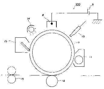
Fig. 2 is a schematic view showing a preferable embodiment of an
electrophotographic apparatus of the present invention. An electrophotographic
apparatus
100 shown in Fig. 2 is provided with a drum-shaped (cylindrical)
electrophotographic
photoreceptor 7 of the invention, provided in a rotatable manner. Around the
electrophotographic photoreceptor 7, there are provided, along a moving
direction of an
external periphery thereof, a charging apparatus 8, an exposure apparatus 10,
a developing
apparatus 11, a transfer apparatus 12, a cleaning apparatus 13 and a charge
eliminator
(erasing apparatus) 14.
A charging apparatus 8 of a corona charging type is used for charging the
electrophotographic photoreceptor 7. The charging apparatus 8 may be
constituted of a
corotron charger or a scorotron charger. The charging apparatus 8 is connected
to a power
source 9.
An exposure apparatus 10 exposes the charged electrophotographic photoreceptor
7
to a light, thereby forming an electrostatic latent image thereon.
A developing apparatus 11 develops the electrostatic latent image with a
developer
to form a toner image. The developer preferably includes toner particles of a
volume
average particle size of 3 to 9 pm, obtained by a polymerization method.
A transfer apparatus 12 transfers the toner image, developed on the
electrophotographic photoreceptor 7, onto a transfer medium.
A cleaning apparatus 13 removes a toner remaining on the electrophotographic
photoreceptor 7 after the transfer. The cleaning apparatus 13 preferably has a
blade
member maintained in contact with the electrophotographic photoreceptor 7
under a linear
pressure of 10 - 150 g/cm.
A charge eliminator (erasing apparatus) 14 erases a retentive charge on the
electrophotographic photoreceptor 7.
The electrophotographic apparatus 100 is provided with a fixing apparatus 15
for
fixing, after the transfer step, the toner image to the transfer medium.
Fig. 3 is a schematic view showing another preferred embodiment of the
electrophotographic apparatus of the invention. An electrophotographic
apparatus 110
shown in Fig. 3 is similar, in structure, to the electrophotographic apparatus
100 shown in
Fig. 2, except that it is equipped with a charging apparatus 8' for chargvig
the
29
CA 02501451 2005-03-18
electrophotographic photoreceptor 7 in a contact method. In the
electrophotographic
apparatus 110 with a contact charging apparatus utilizing a DC voltage
superposed with an
AC voltage, the electrophotographic photoreceptor 7 can be advantageously
employed
because of an excellent leak resistance. In this case, the charge eliminator
14 may not
need to be provided.
In the contact charging method, a charging member of a roller shape, a blade
shape,
a belt shape, a brush shape, a pin-electrode shape, or a magnetic brush shape
can be utilized.
Particularly in case of a roller-shaped or blade-shaped charging member, such
charging
member may be positioned, with respect to the photoreceptor, in a contact
state or in a non-
contact state with a certain gap ( 100 p,m or less) thereto.
A roller-shaped, blade-shaped or belt-shaped charging member is constituted of
a
material regulated to an electrical resistance ( 103 - 10$ SZ) suitable for a
charging member,
and may be constituted of a single layer or plural layers.
It can be formed of an elastomer constituted of a synthetic rubber such as
urethane
rubber, silicone rubber, fluorinated rubber, chloroprene rubber, butadiene
rubber, EPDM or
epichlorohydrin rubber, or of polyolefin, polystyrene or polyvinyl chloride,
blended with an
appropriate amount of a conductivity providing material such as conductive
carbon, a metal
oxide or an ionic conductive material thereby exhibiting an effective
electroconductivity as
a charging member.
It is also possible to prepare a paint of a resin such as nylon, polyester,
polystyrene,
polyurethane or silicone, blending therein an appropriate amount of a
conductivity
providing material such as conductive carbon, a metal oxide or an ionic
conductive material
and laminating thus obtained paint by a suitable method, such as a dip, a
spraying or a roll
coating.
On the other hand, a brush-shaped charging member can be prepared by
subjecting
already known fibers of acrylic resin, nylon or polyester, rendered
electroconductive, to a
fluorine impregnating process and then implanting such fibers using an ali-
eady known
method. The fluorine impregnating process may be executed after the fibers are
formed
into a brush-shaped charging member.
The brush-shaped charging member herein includes a roller-shaped member and a
charging member having fibers planted on a flat plate, and is not limited to a
particular
shape. Also a magnetic brush-shaped charging member includes ferrite or
magnetite,
showing magnetic properties, arranged radially on an external periphery of a
cylinder
incorporating multi-pole magnets, and the ferrite or magnetite is preferably
subjected to a
fluorine impregnating process prior to the formation into a magnetic brush.
CA 02501451 2005-03-18
Fig. 4 is a schematic view showing another preferred embodiment of the
electrophotographic apparatus of the invention. An electrophotographic
apparatus 200 is
of a tandem type with intermediate transfer method. In an housing 220, four
electrophotographic photoreceptors 201a - 201d (for example 201a for yellow
color, 201b
for magenta color, 201c for cyan color and 201d for black color image
formation) are
an-anged mutually parallel and along an intermediate transfer belt 209.
For transferring a visible image onto a transfer sheet such as paper, a
transfer drum
method is already known in which the transfer sheet such as paper is wound on
a transfer
drum and visible images of respective colors on the photoreceptor are
transferred onto such
transfer sheet. In this case, an transfer drum has to be rotated plural turns
for transferring
the visible images from the photoreceptors to the transfer sheet, but, in the
tandem
intermediate transfer method, the transfer from plural photoreceptors 201a -
201d can be
achieved in a single turn of the intermediate transfer member 209. This
transfer method is
promising hereafter because of the higher transfer speed thus achievable and
an advantage
that the transfer medium need not be selective as in the case of the transfer
drum method.
The electrophotographic photoreceptors 201a - 201d mounted in the
electrophotographic apparatus 200 are respectively similar to the
electrophotographic
photoreceptor 7.
The electrophotographic photoreceptors 201 a - 201 d are respectively rotated
in a
predetermined direction (counterclockwise in the illustration), and, charging
rollers 202a -
202d, developing apparatuses 204a - 204d, primary transfer rollers 210a -
210d, and
cleaning apparatuses 215a - 215d are arranged along the direction of rotation.
Toners of
four colors of yellow, magenta, cyan and black, respectively contained in
toner cartridges
205a - 205d, can be respectively supplied to the developing apparatuses 204a -
204d. Also
the primary transfer rollers 210a - 210d are respectively in contact with the
electrophotographic photoreceptors 201a - 201d across the intermediate
transfer belt 209.
In a predetermined position of the housing 220, a laser light source (exposure
apparatus) 203 is positioned. A laser light emitted from the laser light
source 203 is so
guided to irradiate the surfaces of the electrophotographic photoreceptors
201a - 201d after
the charging, whereby steps of charging, exposure, development, primary
transfer and
cleaning are executed in succession in the course of rotation of the
electrophotographic
photoreceptors 201a - 201d, and toner images of the respective colors are
transferred in
superposition onto the intermediate transfer belt 209.
The intermediate transfer belt 209 is supported under a predetermined tension
by a
driving roller 206, a backup roller 208 and a tension roller 207, and is
rendered rotatable
31
CA 02501451 2005-03-18
without slack by the rotation of these rollers. A secondary transfer roller
213 is so
positioned as to contact the backup roller 208 across the intermediate
transfer belt 209.
The intermediate ta~ansfer belt 209, after passing between the backup roller
208 and
the secondary transfer roller 213, is subjected to a surface cleaning by a
cleaning blade 216
positioned for example in the vicinity of the driving roller 206 and is then
used again for a
next image formation process.
A tray (transfer medium tray) 211 is provided in a predetermined position
within
the housing 220, and a transfer medium 230 such as paper contained in the tray
211 is
transferred, by a transfer roller 212, in a path between the intermediate
transfer belt 209 and
the secondary transfer roller 213 and also between mutually contacting two
fixing rollers
214, and is then discharged to the exterior of the housing 220.
In the foregoing, there has been explained a case in which the intermediate
transfer
belt 209 is employed as an intermediate transfer member, but the intermediate
transfer
member may be constructed as a belt shape (for example as an endless belt), as
in the case
of the intermediate transfer belt 209, or as a drum shape. In case of
employing a belt-
shaped structure such as the intermediate transfer belt 209 as the
intermediate transfer
member, such belt preferably has a thickness of 50 to 500 Vim, more preferably
60 to 150
Vim. The thickness of the belt can be suitably selected according the hardness
of the
material. Also in the case of employing a drum-shaped structure as the
intermediate
transfer member, a substrate is preferably constituted of a cylindrical
substrate foamed, for
example, of aluminum, stainless steel (SUS) or copper. On such a cylindrical
substrate, an
elastic layer may be provided if necessary, and a surface layer can be formed
on such an
elastic layer.
The transfer medium mentioned in the invention may be any medium to which a
toner image formed on the electrophotographic photoreceptor is transferred.
For example,
in case of direct transfer from the electrophotographic photoreceptor to a
paper or the like,
such paper or the like constitutes the transfer medium, and, in case of
employing an
intermediate transfer member, such intermediate transfer member constitutes
the transfer
medium.
As the material constituting the aforementioned endless belt, there is
proposed a
semiconductive endless belt of a thermoplastic material such as a
polycarbonate resin (PC),
a polyvinylidene fluoride (PVDF), polyalkylene phthalate, a PC/polyalkylene
phthalate
(PAT) blend, or an ethylene-tetrafluoroethylene copolymer (ETFE).
Also Japanese Patent No. 2560727 and JP-A No. 5-77252 propose an intermediate
transfer member in which ordinary carbon black is dispersed as a conductive
powder in a
32
CA 02501451 2005-03-18
polyimide resin.
An intermediate transfer member that does not easily cause image defects, such
as
color slippage, can be obtained since the polyimide resin, having a high
Young's modulus,
shows little deformation under driviilg (under stresses from the supporting
roller, cleaning
blade and the like). The polyimide resin is usually obtained as a polyamidic
acid solution
by a polymerization reaction of a tetracarboxylic acid dianhydride or a
derivative thereof
with a diamine in approximately equimolar amounts in solvent. The
tetracarboxylic acid
dianhydride is, for example, represented by a following formula (IV):
O
O~ ~R~ ,O ( I U)
O O
In the formula (IV), R represents a tetravalent organic group selected from
the
group of an aliphatic linear hydrocarbon group, an alicyclic hydrocarbon
group, an aromatic
hydrocarbon group, and such hydrocarbon groups to which a substituent is
bonded.
Specific examples of tetracarboxylic acid dianhydride include pyromellitic
acid
dianhydride, 3,3',4,4'-benzophenonetetracarboxylic acid dianhydride, 3,3',4,4'-
biphenyltetracarboxylic acid dianhydride, 2,3,3',4-biphenyltetracarboxylic
acid dianhydride,
2,3,6,7-naphthalenetetracarboxylic acid dianhydride, 1,2,5,6-
naphthalenetetracarboxylic
acid dianhydride, 1,4,5,8-naphthalenetetracarboxylic acid dianhydride, 2,2'-
bis(3,4-
dicarboxyphenyl)sulfonic acid dianhydride, perylene-3,4,9,10-tetracarboxylic
acid
dianhydride, bis(3,4-dicarboxyphenyl) ether dianhydride, and
ethylenetetracarboxylic acid
dianhydride.
On the other hand, specific examples of diamine include 4,4'-diarninodiphenyl
ether, 4,4'-diaminodiphenylmethane, 3,3'-diaminodiphenylmethane, 3,3'-
dichlorobenzidine,
4,4'-diaminodiphenylsulfide, 3,3'-diamii~odiphenylsulfon, 1,5-
diaminonaphthalene, m-
phenylenediamine, p-phenylenediamine, 3,3'-dimethyl-4,4'-biphenyldiamuie,
benzidiiie,
3,3'-dimethylbenzidine, 3,3'-dimethoxybenzidine, 4,4'-diaminodiphenylsulfon,
4,4'-
diaminodiphenylpropane, 2,4-bis([3-amino-tert-butyl)toluene, bis(p-(3-amino-
tert-
butylphenyl)ether, bis(p-(3-methyl-8-aminophenyl)benzene, bis-p-(1,1-dimethyl-
5-
aminopentyl)benzene, 1-isopropyl-2,4-m-phenylenediamine, m-xylilenediamine, p-
xylilenediamine, di(p-aminocyclohexyl)methane, hexamethylenediamine,
heptamethylenediamine, octamethylenediamine, nonamethylenediamine,
33
CA 02501451 2005-03-18
decamethylenediamine, diaminopropyltetramethylene, 3-
methylheptamethylenediamine,
4,4-dimethylheptamethylenediamine, 2,11-diaminododecane, 1,2-bis-3-
aminopropoxyethane, 2,2-dimethylpropylenediamine, 3-
methoxyhexamethylenediamine,
2,5-dimethylheptamethylenediamine, 3-methylheptamethylenediamine, 5-
methylnonamethylenediamine, 2,17-diaminoeicosadecane, 1,4-diaminocyclohexane,
1,10-
diamino-1,10-dimethyldecane, 12-d iaminooctadecane, 2,2-bis[4-(4-
aminophenoxy)phenyl]propane, piperadine, HZN(CH,)3°(CHZ)ZO(CH,)NH,,
HZN(CHZ)3S(CHz)3NH2, and HZN(CH~)3N(CH3)2(CHz)3NH,.
The solvent to be used in the polymerization reaction of the tetracarboxylic
acid
dianhydride and the diamine is advantageously a polar solvent in consideration
of solubility
and the like. The polar solvent is preferably an N,N-dialkylamide, and more
specifically
of a lower molecular weight, such as N,N-dimethylformamide, N,N-
dimethylacetamide,
N,N-diethylformamide, N,N-diethylacetamide, N,N-dimethylmethoxyacetamide,
dimethylsulfoxide, hexamethylphosphonyltriamide, N-methyl-2-pywolidone,
pyridine,
tetramethylenesulfone and dimethyltetramethylenesulfone. Such solvents may be
employed singly or in a combination of two or more kinds.
The intermediate transfer member contains oxidation-processed carbon black in
a
polyimide resin. The oxidation-processed carbon black can be obtained by an
oxidation
process of carbon black thereby providing the surface thereof with an oxygen-
containing
functional group (such as a carboxyl group, a quinone group, a lactone group
or a hydroxyl
group).
Such an oxidation process can be achieved for example by an air oxidation
method
of contacting and reacting with air in a high-temperature environment, a
method of
contacting with a nitrogen oxide or ozone at normal temperature, or a method
of ozone
oxidation at a low temperature after air oxidation at a high temperature.
Examples of oxidized carbon include products of Mitsubishi Chemical
Corporation
such as MA100 (pH 3.5, volatiles 1.5%), MAl00R (pH 3.5, volatiles 1.5%),
MAl00S (pH
3.5, volatiles 1.5%), #970 (pH 3.5, volatiles 3.0%), MAl l (pH 3.5, volatiles
2.0%), #1000
(pH 3.5, volatiles 3.0%), #2200 (pH 3.5, volatiles 3.5%), MA230 (pH 3.0,
volatiles 1.5%),
MA220 (pH 3.0, volatiles 1.0%), #2650 (pH 3.0, volatiles 8.0%), MA7 (pH 3.0,
volatiles
3.0%), MA8 (pH 3.0, volatiles 3.0%), OIL7B (pH 3.0, volatiles 6.0%), MA77 (pH
2.5,
volatiles 3.0%), #2350 (pH 2.5, volatiles 7.5%), #2700 (pH 2.5, volatiles
10.0%), and #2400
(pH 2.5, volatiles 9.0%); those of Degussa AG such as Printex 150T (pH 4.5,
volatiles
10.0%), Special Black 350 (pH 3.5, volatiles 2.2%), Special Black 100 (pH 3.3,
volatiles
2.2%), Special Black 250 (pH 3.1, volatiles 2.0%), Special Black 5 (pH 3.0,
volatiles
34
CA 02501451 2005-03-18
15.0%), Special Black 4 (pH 3.0, volatiles 14.0%), Special Black 4A (pH 3.0,
volatiles
14.0%), Special Black S50 (pH 2.8, volatiles 2.5%), Special Black 6 (pH 2.5,
volatiles
18.0%), Color Black FW200 (pH 2.5, volatiles 20.0%), Color Black FW2 (pH 2.5,
volatiles
16.5%), Color Black FW2V (pH 2.5, volatiles 16.5%); and products of Cabot
Coip. such as
Monarch 1000 (pH 2.5, volatiles 9.5%), Monarch 1300 (pH 2.5, volatiles 9.5%),
Monarch
1400 (pH 2.5, volatiles 9.0%), Mogul-L (pH 2.5, volatiles 5.0%), and Regal
4008 (pH 4.0,
volatiles 3.5%).
Such carbon black obtained by oxidation processing is less susceptible to the
influence of oxidation, which is caused by locally excessive cunent under
repeated voltage
applications. Also the oxygen-containing functional group present on the
surface increases
the dispersibility in the polyimide resin, reducing fluctuations in
resistance, and dependence
on the electric field, thereby decreasing the chance of electric field
concentration by the
transfer voltage.
As a result, there can be obtained an intermediate transfer member capable of
preventing a resistance decrease caused by the transfer voltage, improving the
uniformity of
electrical resistance, showing a reduced dependence on the electric field,
also showing
reduced change in the resistance due to the environment, and providing a high
image quality,
with reduced image defects such white skipped areas in portions of a job run.
In the case
where at least two kinds of the oxidation-processed carbon black are included,
such
oxidation-processed carbon blacks are preferably substantially different in
electroconductivity, and different in physical properties such as a level of
oxidation process,
DBP oil absorption or BET specific surface area based on nitrogen adsorption.
In the case of adding two or more carbon blacks different in physical
properties, it
is possible, for example, to at first add a carbon black providing a high
conductivity and
then to add a carbon black providing a low conductivity, thereby regulating
the surface
resistivity or the like.
Specific examples of the oxidation-processed carbon black include Special
Black 4
(manufactured by Degussa ACS pH 3.0, volatiles 14.0%) and Special Black 250
(manufactured by Degussa AG, pH 3.1, volatiles 2.0%). A content of such
oxidation-
processed carbon black is preferably 10 to 50 weight%, more preferably 12 to
30 weight%
with respect to the polyimide resin. A content less than 10 weight% may
deteriorate the
uniformity of the electrical resistance, thereby resulting in a large loss in
the surface
resistivity with long-teen use, while, at a content exceeding 50 weight%, a
desired
resistance may be difficult to obtain and a molded product may become
undesirably brittle.
An intermediate transfer member of a polyimide resin in which an oxidation-
CA 02501451 2005-03-18
processed carbon black is dispersed can be obtained by a step of preparing a
polyamidic
acid solution in which an oxidation-processed carbon black is dispersed, a
step of forming a
film (layer) on an internal periphery) of a cylindrical mold, and a step of
imidation.
For producing a polyamidic acid solution in which two or more types of the
oxidation-processed carbon black are dispersed, there is conceived a method of
dissolving
and polymerizing the acid dianhydride component and the diamine component, in
a
dispersion liquid iii which two or more types of the oxidation-processed
carbon black are
dispersed in advance in a solvent, and a method of dispersing two or more
types of the
oxidation-processed carbon black respectively in solvents thereby preparing
two or more
carbon black dispersion liquids, then dissolving and polymerizing the acid
dianhydride
component and the diamine component in each dispersion liquid, and mixing the
polyamidic acid solutions, and such methods are suitably selected to obtain a
polyamidic
acid solution in which carbon black is dispersed.
The polyamidic acid solution thus obtained is supplied and developed on an
internal
periphery of a cylindrical mold to form a film, which is then heated to
execute an imidation
of the polyamidic acid. In such an imidation heating step, an intermediate
transfer member
with satisfactory surface flatness can be obtained by executing an imidation
under a heating
condition of maintaining a constant temperature for 0.5 hours or longer. In
the following,
this process will be explained in detail.
At first a polyamidic acid solution is supplied onto an internal periphery of
a
cylindrical mold. Such supplying method can be suitable selected such as a
supply by a
dispenser or by a die. The surface of the internal periphery of the
cylindrical mold
employed in this step is preferably mirror-finished.
Then thus supplied polyamidic acid solution is formed into a film of a uniform
thickness, for example by a centrifugal molding method under heating, a
molding method
with a bullet-like runner, or a rotation molding method. Subsequently there
can be
executed a process of heating the mold bearing the film on the internal
periphery thereof in
a dryer to a temperature causing imidation, or a process of eliminating the
solvent until the
film can sustain a belt shape, then peeling the film from the internal
periphery of the mold
and placing the film on an external periphery of a metal cylinder, and heating
the film
together with the metal cylinder thereby achieving imidation. In order to
obtain an
intermediate transfer member satisfactory in the flatness and the precision of
the external
surface, a method of eliminating the solvent until the film can sustain a belt
shape, then re-
placing the film on an extei~i~ial periphery of the metal cylinder, and
executing imidation, is
preferable.
36
CA 02501451 2005-03-18
A heating condition in the solvent eliminating step is not particularly
restricted as
long as the solvent can be elimuiated, but is preferably 0.5 to 5 hours at 80
to 200°C. Then
a molded substance, which can now sustain the foam as a belt, is peeled off
from the internal
periphery of the mold. In this operation, a releasing treatment may be applied
to the
internal periphery of the mold.
Then the molded substance, which is heated and cured until it can sustain the
form
of a belt, is re-fitted on an external periphery of a metal cylinder and is
heated together with
such a metal cylinder, thereby causing an imidation reaction of the polyamidic
acid.
The metal cylinder to be employed in this step preferably has a linear
expansion
coefficient larger than that of polyimide resin and is given an external
diameter somewhat
smaller than the internal diameter of the polyimide molded substance, thereby
achieving
thermal setting and obtaining a uniform endless belt of a uniform thickness.
The metal
cylinder to be employed in this step preferably has a surface roughness (Ra)
on the external
surface of 1.2 to 2.0 p.m. In case the metal cylinder has a surface roughness
(Ra) less than
1.2 ~tm on the external surface, the obtained belt-shaped intermediate
transfer member
may not cause slippage by shrinkage in the axial direction of the metal
cylinder, because the
metal cylinder itself is excessively flat, whereby drawing may occur resulting
in
fluctuations in the film thickness and a deteriorated precision of the
flatness.
On the other hand, in case the metal cylinder has a surface roughness (Ra)
exceeding 2.0 ~m on the external surface, the external surface pattern of the
metal cylinder
may be transferred onto the internal surface of the belt-shaped intermediate
transfer member
and may generate irregularities on the external surface thereof, thus inducing
image defects.
A belt-shaped intermediate transfer member thus prepared of polyimide resin in
which
carbon black is dispersed has a surface roughness (Ra) of 1.5 ~tm or less on
the external
surface.
The surface roughness is measured according to JIS B601, the disclosure of
which
is incorporated by reference herein. A surface roughness (Ra) of the
intermediate transfer
member exceeding 1.5 ~m may induce an image defects such as mottled images.
This is
presumably because an electric field, caused by the voltage applied at the
transfer step or by
a peeling charging, is locally concentrated on protruding portions of the
belt, modifying the
surface of such portions, thereby generating a new conductive path with a
lower resistance
and inducing a lower image density, thus giving a mottled impression on the
entire image.
The heating step for imidation is conducted preferably with a heating
temperature
of 220 to 280°C and a heating time of 0.5 to 2 hours. The slwinkage at
imidation becomes
largest with heating conditions of such a range, though it is dependent also
on the
37
CA 02501451 2005-03-18
composition of the polyimide resin, thereby achieving a gradual shrinkage of
the belt in the
axial direction thereof, thus avoiding fluctuations of the film thickness and
the deterioration
in the precision of flatness.
The intermediate transfer member after such a heating step has a flatness of 5
mm
or less, preferably 3 mm or less. A flatness of 5 mm or less causes no
mottling and little
slippage among the colors. However, in case an edge portion of the belt is
curled upward
or downward, the belt with a flatness of 5 mm or less may occasionally leave a
trace of
contact with components in the vicinity, though such a belt does not show
breakage in the
course of use. An intermediate transfer member with a flatness of 3 mm or less
does not
cause contact with the components in the vicinity and scarcely shows slippage
in the colors.
(Process cartridge)
In the following there will be explained a process cartridge incorporating an
electrophotographic photoreceptor of the invention.
Fig. 5 is a schematic view showing a preferred embodiment of the process
cartridge
of the invention.
A process cartridge 300 incorporates, within a case 301, an
electrophotographic
photoreceptor 7, a charging apparatus 8, a developing apparatus 11, a cleaning
apparatus 13
and a charge eliminator 14 which are combined and integrated with a rail 303.
The
process cartridge 300 is not equipped with an exposure apparatus, but has an
aperture 305
for exposure in the case 301.
Further, the electrophotographic photoreceptor 7 is the above-mentioned
electrophotographic photoreceptor of the invention, which is an
electrophotographic
photoreceptor 7 which comprises on an electroconductive substrate, an
uiterlayer and a
photosensitive layer comprising a charge-generating layer and a charge-
transporting layer
on the substrate, wherein the interlayer comprises fine metal oxide particles
and the
interlayer and the charge-generating layer comprise an anthraquii~one
derivative.
Such a process cartridge 300 is detachably mounted on a main body of an
electrophotographic apparatus including a transfer apparatus 12, a fixing
apparatus 15 and
unillustrated other components, and constitutes an electrophotographic
apparatus together
with such a main body
(Examples)
Hereinbelow, the present invention is described in more detail by means of the
following Examples, but these examples are not intended to limit the
invention.
(Example 1 )
15 parts by weight of a polyvinylbutyral resin (S-Lec BM-S, manufactured by
38
CA 02501451 2005-03-18
Sekisui Chemical Co., Ltd.) and 20 parts by weight of a hardening agent
(BL3475,
manufactured by Sumitomo Bayer Urethane Co., Ltd.) are dissolved in 80 parts
by mass of
2-butanone, to which are added 90 parts by mass of zinc oxide powders (SMZ-
017N 10,
manufactured by Tayca Corp.) and 3 parts by mass of 1-hydroxyanthraquinon, and
the
mixture is stirred. Using a Dyno-Mill dispersion device (manufactured by
Shinmaru
Enterprise Co.), the mixture is dispersion treated for 4 hours. To the
obtained solution is
added fine silicone particles (R935: average particle diameter 5.0 Vim,
manufactured by
Toray Fine Chemicals Co., Ltd.) until a 5% solution, by volume based on all
solid content
of the solution, is obtained as a coating solution for the interlayer.
Then, a mixture consisting of 3 parts by mass of hydroxygallium
phthalocyanine,
which when examined by X-ray diffractometry with a CuI~ a ray, gives a
diffraction
spectrum having diffi~action peaks at Bragg angles (28 ~ 0.2°) of
7.5°, 9.9°, 12.5°, 16.3°,
18.6°, 25.1 ° and 28.1°, 2 parts by mass of a vinyl
chloride/vinyl acetate copolymer (VMCH,
manufactured by Nippon Unicar Co., Ltd.), and 180 parts by mass of butyl
acetate is
subjected to dispersion treatment using a sand mill for 2 hours. Further, 0.05
parts by
mass of 1,2-diaminoanthraquinone is added to obtain a coating solution for a
charge-
generating layer.
Further, as a charge-transporting material, 4 parts by weight of N,N'-bis(3,4-
dimethylphenyl)biphenyl-4-amine and 6 parts by weight of a bisphenol Z-type
polycarbonate resin (manufactured by Mitsubishi Chemical Corp.: Yupilon Z400),
0.2 parts
by weight of 2,6-di-t-butyl-4-methylphenol are added and dissolved in 60 parts
by weight of
a mixed solvent of tetrahydrofuran (THF) and toluene to obtain a coating
solution for a
charge-transporting layer.
ED pipe aluminum (30 mm~) is used for the electroconductive support. An
interlayer coating solution is dip coated on the aluminum support in a film
thickness of 30
~tm.
Further, the interlayer is formed by drying at 150°C for 60
minutes.
Subsequently, the charge-generating layer coating solution is dip coated on
the
interlayer with the film thickness of 0.2 pm to form a charge-generating
layer.
Then, the charge-transporting layer coating solution is coated on the charge-
generating layer, and is dried at 120°C for 40 minutes to form a charge-
transporting layer
with a film thickness of 20 ~tm.
Thereby, an electrophotographic photoreceptor comprising 3 layers is obtained.
(Example 2)
39
CA 02501451 2005-03-18
An electrophotographic photoreceptor is obtained in the similar manner as in
Example 1 except that an anthraquinone derivative to be added to the charge-
generating
layer is the same compound (1-hydroxyantlu-aquinone) as in the interlayer.
(Example 3)
An electrophotographic photoreceptor is obtained in the similar manner as in
Example 1 except that a compound to be added to the interlayer is alizarin,
and a compound
to be added to the charge-generating layer is I-hydroxyanthraquinone.
(Example 4)
An electrophotographic photoreceptor is obtained in the similar manner as in
Example 1 except that a compound to be added to the interlayer and the charge-
generating
layer is alizarin.
(Comparative Example 1)
An electrophotographic photoreceptor is obtained in the similar manner as in
Example 1 except that 3 parts by weight of the below-described pyrazine-based
compound
is added only to the interlayer without adding the anthraquinone-based
compound to the
interlayer or the charge-generating layer. In addition, the below-described
pyrazine-based
compound possesses electron acceptor properties in the similar manner as in
the
anthraquinone derivative.
~N CN
w
~N CN
I
R
(R : Pheny L Groupl
(Comparative Example 2)
An electrophotographic photoreceptor is obtained in the similar manner as in
Example I except that 0.05 parts by weight of the above-described pyrazine-
based
compound is added only to the charge-generating layer without adding the
anthraquinone-
based compound to the interlayer and the charge-generating layer.
(Comparative Example 3)
An electrophotographic photoreceptor is obtained in the similar manner as in
Example 1 except that 3 parts by weight of the above-described pyrazine-based
compound
is added to the interlayer and 0.05 parts by weight of the pyrazine-based
compound is added
to the charge-generating layer without adding the anthraquinone-based compound
to the
CA 02501451 2005-03-18
iiterlayer and the charge-generating layer.
(Comparative Example 4)
An electrophotographic photoreceptor is obtained in the similar manner as in
Example 1 except that alizarin is added only to the charge-generating layer,
nat to the
interlayer.
(Comparative Example 5)
An electrophotographic photoreceptor is obtained in the similar manner as in
Example 1 except that the dispersion time of a coating fluid to the interlayer
is set as 30
minutes.
(Comparative Example 6)
An electrophotographic photoreceptor is obtained in the similar manner as in
Example 1
except that the dispersion time of a coatilg fluid to the interlayer is set as
20 hours.
(Comparative Example 7)
An electrophotographic photoreceptor is obtained in the similar manner as in
Example 1 except that an anthraquinone derivative is not added to the
interlayer and the
charge-generating layer.
(Measurement of Surface Potential of Electrophotographic Photoreceptor)
Electrophotographic photoreceptors of the Examples and Comparative Examples
are mounted on a modified full-color printer DocuCenter Color 400CP (contact
charging
method, tandem method), manufactured by Fuji Xerox Co., Ltd, and the surface
potentials
of the photoreceptor after charging and exposure are measured in the machine.
The
modified DocuCenterColor400CP is modified so that measuring of the surface
potential of
the photoreceptor in the machine can be carried out.
In addition, a continuous printing test is conducted at an image density of
5%, in
which 50000 sheets of paper are printed, and the potential after the
continuous printing is
measured.
(Measurement of Volume Resistivity of Interlayer)
A coating solution for the interlayer is dip coated on an aluminum substrate,
and is
dried and hardened at 150°C for 60 minutes to fomn an interlayer (film
thickness: 30 Vim).
To the interlayer, an electric field of 106 V/m is applied thereto using a ~ 1-
mm gold
electrode as a counter electrode to measure the current values after 10
seconds and to
determine a resistance of the interlayer at that time.
The resistance value is divided by the volume of the interlayer in the
measured
portion (- electrode area (qtr'-) x film thickness (30 pm)) to calculate the
volume resistivity
of the invention. The measurement is conducted at 28°C and 85% RH
humidity.
41
CA 02501451 2005-03-18
The obtained results are shown in Table 1 I.
[Table 11 ]
Initial Surface
Charge- Volume
Interlayer surface potential
generating resistivity
additive potential after running
layer additive(S2~cm)
(V) (V)
Ex. 1 (A-2) (B-5) 5.7 x 10' 70 245
Ex. 2 (A-2) (B-2) 5.4 x 10' 67 241
Ex. 3 (A-7) (B-2) 5.4 x 10' 63 245
Ex. 4 (A-7) (B-7) 5.5 x 10' 57 230
Pyrazine-based
Comp. Ex. - 5.4 x 10' 78 288
1
compound
Pyrazine-based
Comp. Ex. - 5.6 x 10' 80 285
2
compound
Pyrazine-basedPyrazine-based
Comp. Ex. 5.4 x 10' 77 280
3
compound compound
Comp. Ex. - (B-7) 5.8 x 10' 78 286
4
Comp. Ex. (A-2) (B-2) 8.8 x 10' 70 235
Comp. Ex. (A-2) (B-2) 1.2 x 10" 92 388
6
Comp. Ex. - - 5.6 x 10' 85 324
7
Note: In the comparative example 5, fogging occurs.
(Conclusions)
Examples 1 to 4 of the invention, as compared to the Comparative Examples, can
reduce the surface potential by elevating sensitivity of the photoreceptor.
Further, by
adding an anthraquinone derivative to both layers, the increase in the
residual potential even
after the job run can be inhibited.
Meanwhile, when a pyrazine-based compound is added to the interlayer as
described in Comparative Example 1, the charge-generating layer as described
in
Comparative Example 2 and both layers as described in Comparative Example 3,
the
surface potential of the photoreceptor is high, and an increase in the
potential due to the
residual potentials is observed after the running.
42
CA 02501451 2005-03-18
In Comparative Example 6, wherein the volume resistivity of the interlayer is
higher than the range disclosed in the invention, the effect of reducing the
potential is not
confirmed. Further, in Comparative Example 5, wherein the volume resistivity
was lower
than the range disclosed in the present invention, the effect of reducing the
potential is
observed, but image irregularities (fogging) occurs.
43