Language selection

Search

Patent 2502104 Summary

Third-party information liability

Some of the information on this Web page has been provided by external sources. The Government of Canada is not responsible for the accuracy, reliability or currency of the information supplied by external sources. Users wishing to rely upon this information should consult directly with the source of the information. Content provided by external sources is not subject to official languages, privacy and accessibility requirements.

Claims and Abstract availability

Any discrepancies in the text and image of the Claims and Abstract are due to differing posting times. Text of the Claims and Abstract are posted:

  • At the time the application is open to public inspection;
  • At the time of issue of the patent (grant).
(12) Patent Application: (11) CA 2502104
(54) English Title: ARRANGEMENT OF A DATA COUPLER FOR POWER LINE COMMUNICATIONS
(54) French Title: CONFIGURATION D'UN COUPLEUR DE TRANSMISSION DE DONNEES POUR LA TRANSMISSION DE DONNEES SUR DES LIGNES ELECTRIQUES
Status: Dead
Bibliographic Data
(51) International Patent Classification (IPC):
  • H04M 11/04 (2006.01)
  • H01F 38/20 (2006.01)
  • H01P 1/32 (2006.01)
  • H04B 3/56 (2006.01)
(72) Inventors :
  • CERN, YEHUDA (United States of America)
(73) Owners :
  • AMBIENT CORPORATION (United States of America)
(71) Applicants :
  • AMBIENT CORPORATION (United States of America)
(74) Agent: GOWLING LAFLEUR HENDERSON LLP
(74) Associate agent:
(45) Issued:
(86) PCT Filing Date: 2003-10-17
(87) Open to Public Inspection: 2004-04-29
Availability of licence: N/A
(25) Language of filing: English

Patent Cooperation Treaty (PCT): Yes
(86) PCT Filing Number: PCT/US2003/033080
(87) International Publication Number: WO2004/036772
(85) National Entry: 2005-04-12

(30) Application Priority Data:
Application No. Country/Territory Date
60/419,174 United States of America 2002-10-17

Abstracts

English Abstract


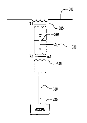
An arrangement for coupling data between a power line (300) and a
communication device (325) includes an inductive coupler (305) that employs a
power line conductor as a primary winding, a capacitor (310) connected across
a secondary winding of the inductive coupler (305) for creating a resonant
circuit with the secondary winding at a frequency within a desired frequency
band, and an impedance matching transformer (315) for connecting a
communications device (325) to the secondary winding. The resonant circuit has
a loaded Q consistent with the desired bandwidth. An alternative arrangement
includes a capacitor (410) in series with conductive cylinder section (505)
and (510) between the power line and communication device (435), where the
capacitor is for blocking power line voltage while passing a signal between
the power line and the communication device, and the conductive cylinder
sections (505) and (510) appears as a low inductance to the signal.


French Abstract

L'invention concerne une configuration de composants destinés au couplage de données entre une ligne électrique et un dispositif de communication. Cette configuration comprend un coupleur inductif utilisant un conducteur de ligne électrique comme enroulement primaire, un condensateur relié par un second enroulement du coupleur inductif servant à créer un circuit résonant avec l'enroulement secondaire à une fréquence comprise dans une bande de fréquence désirée, et un transformateur adaptateur d'impédance servant à connecter un dispositif de communication à l'enroulement secondaire. Le circuit résonant a une atténuation effective correspondant à la bande passante désirée. Un autre mode de réalisation de cette configuration comprend un condensateur monté en série avec une bobine conductrice entre la ligne électrique et le dispositif de communication, le condensateur étant utilisé pour bloquer la tension de la ligne électrique et pour laisser passer un signal entre la ligne électrique et le dispositif de communication, la bobine conductrice offrant une faible inductance par rapport au signal.

Claims

Note: Claims are shown in the official language in which they were submitted.


WHAT IS CLAIMED IS:


1. A method for configuring components for power line communications,
comprising:
installing an inductive coupler that employs a power line conductor as a
primary winding;
connecting a capacitor across a secondary winding of said inductive coupler
for creating a resonant circuit with said secondary winding at a
frequency within a desired frequency band; and
connecting a communications device to said secondary winding via an
impedance matching transformer,
wherein said resonant circuit has a loaded Q consistent with said desired
bandwidth.

2. A method for coupling data between a power line and a communication
device, comprising:
installing a capacitor in series with a conductive cylinder between said
power line and said communication device,
wherein said capacitor is for blocking power line voltage while passing a
signal between said power line and said communication device, and
wherein said conductive cylinder appears as a low inductance to said signal.

3. The method of claim 2, further comprising installing a high interruption
current fuse in series with said capacitor.

4. An arrangement of components for coupling data between a power line
and a communication device, comprising:
an inductive coupler that employs a power line conductor as a primary
winding;

7


a capacitor connected across a secondary winding of said inductive coupler
for creating a resonant circuit with said secondary winding at a
frequency within a desired frequency band; and
an impedance matching transformer for connecting a communications device
to said secondary winding,
wherein said resonant circuit has a loaded Q consistent with said desired
bandwidth.

5. An arrangement of components for coupling data between a power line
and a communication device, comprising:
a capacitor in series with a conductive cylinder between said power line and
said communication device,
wherein said capacitor is for blocking power line voltage while passing a
signal between said power line and said communication device, and
wherein said conductive cylinder appears as a low inductance to said signal.

6. The arrangement of claim 5, further comprising a high interruption current
fuse in series with said capacitor.

8


Description

Note: Descriptions are shown in the official language in which they were submitted.


CA 02502104 2005-04-12
WO 2004/036772 PCT/US2003/033080
ARRANGEMENT OF A DATA COUPLER FOR POWER LINE
COMMUNICATIONS
BACKGROUND OF THE INVENTION
S
1. Field of the Invention
The present invention relates to power line communications, and more
particularly, to configurations of data couplers for power line
communications.
2. Description of the Related Art
A data coupler for power line communications couples a data signal
between the power line and a communication device such as a modem. The data
coupler exhibits a cutoff frequency. Below the cutoff frequency, coupling
attenuation between the power line and the communication device becomes
excessive. The data coupler may be either an inductive coupler or a capacitive
coupler.
An inductive coupler for a power line should ideally have a magnetization
inductance with an impedance that is large as compared to an impedance of the
communication device. As the magnetization inductance is in shunt with a
signal
and inductively loads the signal, a low magnetization inductance is
undesirable.
A capacitive coupler may be efficient for use on a power line, especially a
low voltage line.
FIG. 1 is a schematic of a prior art capacitive coupler as may be used to
couple a power line modem to a secondary power line. A power line 400,
nominally neutral, is connected to a shield terminal of a coax connector 420.
A
power line 405, nominally an energized phase line, is connected to a center
1


CA 02502104 2005-04-12
WO 2004/036772 PCT/US2003/033080
conductor contact of connector 420 via a fuse 415 and a capacitor 410. A modem
435 is connected, via a cable 430 and a connector 425, to connector 420. The
capacitive coupler thus couples high frequency signals between modem 435 and
power lines 400 and 405.
The value of capacitor 410 is several nanofarads, large enough to have
negligible reactance at signal frequency and small enough to have a large
reactance at power frequency.
A ceramic capacitor with an appropriate dielectric may be used in such a
coupler and provides a low impedance to signal frequencies in the MHz range.
However, a lead connecting such a capacitor to the power line may be
relatively
long, and may have an impedance far exceeding the capacitor's impedance at
signal frequencies.
For example, wires in a low voltage rack arrangement are typically spaced
centimeters (cm) apart, and a 10 AWG wire of that length has an inductance of
0.21 microhenry (uH) or nearly 40 ohms at 30 megahertz (MHz). Should the
capacitive coupler need to connect to a non-adjacent wire, the impedance could
20 increase to 80 or 120 ohms. As a typical capacitive coupler must be fused,
and a
fuse impedance is added in series, a total series inductive impedance can be
significant in comparison to a typical modem's 50 ohm impedance.
SUMMARY OF THE INVENTION
There is provided an arrangement of components for coupling data between
a power line and a communication device. The arrangement includes an inductive
coupler that employs a power line conductor as a primary winding, a capacitor
connected across a secondary winding of the inductive coupler for creating a
resonant circuit with the secondary winding at a frequency within a desired
frequency band, and an impedance matching transformer for connecting a
2


CA 02502104 2005-04-12
WO 2004/036772 PCT/US2003/033080
communications device to the secondary winding. The resonant circuit has a
loaded Q consistent with the desired bandwidth.
An alternative arrangement includes a capacitor in series with a conductive
cylinder between the power line and the communication device, where the
capacitor is for blocking power line voltage while passing a signal between
the
power line and the communication device, and the conductive cylinder appears
as
a low inductance to the signal.
BRIEF DESCRIPTION OF THE DRAWINGS
FIG. 1 is a schematic of a prior art capacitive coupler.
FIG. 2 is a schematic of an impedance matching circuit for an inductive
coupler.
FIG. 3 illustrates a circuit with a capacitive coupler using low-inductance
leads.
FIG. 4 is a schematic diagram of the circuit shown in FIG. 3.
DESCRIPTION OF THE INVENTION
A low frequency inductive coupler in accordance with the present invention
extends cutoff frequency downwards, to a lower frequency, without resorting to
an
addition of heavy magnetic cores. The inductive coupler is clamped around an
energized power line conductor of the power line. Assume that the power line
conductor passing through a core of the coupler serves as a primary winding
for
the inductive coupler. Since the coupler is clamped around the power line
conductor, and since the power line conductor serves as a primary winding, the
coupler has only a one-turn primary winding. The physical dimensions of the
3


CA 02502104 2005-04-12
WO 2004/036772 PCT/US2003/033080
power line conductor typically require that the core be large with a long
magnetic
circuit path. An air gap may be required to prevent saturation of the core.
Both of
these factors reduce the inductance of the coupler.
A classic method of reducing reactive loading in a circuit is to resonate an
offending reactance with an opposite reactance. In the case of an inductive
coupler with a shunt inductance, a shunt capacitor may be connected across a
secondary coil of the inductive coupler to neutralize magnetization
inductance.
In the case of a broadband modem, such as those using spread spectrum, the
resonance is likely to be too sharp, and thus is effective over too narrow a
sub-
band. As described herein, an impedance matching transformer is connected
between the coupler and a modem so as to adjust the modem's impedance, as
reflected across the coupler circuit, to provide a low enough loaded Q as to
increase bandwidth so as to be similar to a width of the modem frequency band.
FIG. 2 shows an impedance-matching circuit through which a modem 325 is
connected to an inductive coupler 305. A power line 300 passes through a core
of
inductive coupler 305. A signal transformer 315, with turns ratio n:l,
improves
impedance matching between inductive coupler 305 and modem 325. The
combination of inductive coupler 305 and signal transformer 315 can provide a
very wide bandpass, but the low frequency response of the combination will be
limited to that determined by a magnetization inductance of inductive coupler
305
and an impedance 330 that is reflected from modem 325.
Capacitor 310 resonates the magnetization inductance and provides a
frequency band around the resonant frequency where a loading effect of the
magnetization inductance is reduced, and signal attenuation across inductive
coupler 305 is reduced. The effect of capacitor 310 is to lower the cutoff
frequency of inductive coupler 305, allowing inductive coupler 305 to operate
at a
4


CA 02502104 2005-04-12
WO 2004/036772 PCT/US2003/033080
lower frequency than would otherwise be possible with a given level of
magnetization inductance.
There is thus provided a method for configuring an inductive coupler to a
communication device. The method includes connecting a capacitor across a
secondary winding of the inductive coupler for creating a resonant circuit
with the
secondary winding at a frequency within a desired frequency band, and
connecting
the communications device to the secondary winding via an impedance matching
transformer. The resonant circuit has a loaded Q consistent with the desired
bandwidth.
FIG. 3 is an illustration of a physical implementation of a capacitive coupler
500. Power lines 400 and 405, capacitor 410, fuse 415 and connector 420 retain
the same identification as in FIG. 1. Also as in FIG. 1, modem 435 is
connected,
via cable 430 and connector 425, to connector 420. Electrically conductive
cylinder sections 505 and 510 each have a diameter in the range of 1 to 3 cm,
which is many times larger than diameters of wires, and thus provide
connections
to power lines 400 and 405 with negligible inductance. Conductive cylinder
sections 505 and 510 and an insulating cylinder segment 515 form a
mechanically
rigid body, which may have a common axis.
Power line 400, i.e., a neutral line, is usually bare, otherwise, a few cm of
its
insulation needs to be removed. One end of capacitive coupler 500 is
electrically
connected to, and physically supported by, power line 400. A bar 550 with a
slot
560 and a wing nut 565 provide a mechanism for tightening section 505 onto
power line 400.
The other end of capacitive coupler 500 is electrically connected to power
line 405 by a wire 520 and a clamp 525. Wire 520 is soldered or brazed to
conductive cylinder section 510, and has sufficient stiffness and strength to
support capacitive coupler 500 on power line 405, should upper support
provided


CA 02502104 2005-04-12
WO 2004/036772 PCT/US2003/033080
by the combination of bar 550, slot 560 and wing nut 565, or wire 400, fail.
Clamp 525 is a standard clamp, commonly available to utility linemen.
FIG. 4 is a schematic diagram of the arrangement shown in FIG. 3. Cable
430, connectors 425 and 420, capacitor 410, fuse 415, and conductors 505 and
510
provide a signal path between modem 435 and power lines 400 and 405. Because
of their relatively large diameters, conductive cylinder sections 505 and 510
exhibit inductances that are negligible in comparison to the impedance of
modem
435 and capacitor 410, thus reducing coupling loss.
There is thus provided a method for coupling data between a power line and
a communication device. The method includes installing a capacitor in series
with
a conductive cylinder between the power line and the communication device. The
capacitor is for blocking power line voltage while passing a signal between
the
power line and the communication device, and the conductive cylinder appears
as
a low inductance to the signal. Additionally, the method may include
installing a
high interruption current fuse in series with the capacitor.
It should be understood that various alternatives, combinations and
modifications of the teachings described herein could be devised by those
skilled
in the art. The present invention is intended to embrace all such
alternatives,
modifications and variances that fall within the scope of the appended claims.
6

Representative Drawing
A single figure which represents the drawing illustrating the invention.
Administrative Status

For a clearer understanding of the status of the application/patent presented on this page, the site Disclaimer , as well as the definitions for Patent , Administrative Status , Maintenance Fee  and Payment History  should be consulted.

Administrative Status

Title Date
Forecasted Issue Date Unavailable
(86) PCT Filing Date 2003-10-17
(87) PCT Publication Date 2004-04-29
(85) National Entry 2005-04-12
Dead Application 2009-10-19

Abandonment History

Abandonment Date Reason Reinstatement Date
2008-10-17 FAILURE TO PAY APPLICATION MAINTENANCE FEE
2008-10-17 FAILURE TO REQUEST EXAMINATION

Payment History

Fee Type Anniversary Year Due Date Amount Paid Paid Date
Application Fee $400.00 2005-04-12
Maintenance Fee - Application - New Act 2 2005-10-17 $100.00 2005-04-12
Registration of a document - section 124 $100.00 2006-03-22
Maintenance Fee - Application - New Act 3 2006-10-17 $100.00 2006-10-17
Maintenance Fee - Application - New Act 4 2007-10-17 $100.00 2007-10-17
Owners on Record

Note: Records showing the ownership history in alphabetical order.

Current Owners on Record
AMBIENT CORPORATION
Past Owners on Record
CERN, YEHUDA
Past Owners that do not appear in the "Owners on Record" listing will appear in other documentation within the application.
Documents

To view selected files, please enter reCAPTCHA code :


To view images, click a link in the Document Description column. To download the documents, select one or more checkboxes in the first column and then click the "Download Selected in PDF format (Zip Archive)" or the "Download Selected as Single PDF" button.

List of published and non-published patent-specific documents on the CPD .

If you have any difficulty accessing content, you can call the Client Service Centre at 1-866-997-1936 or send them an e-mail at CIPO Client Service Centre.


Document
Description 
Date
(yyyy-mm-dd) 
Number of pages   Size of Image (KB) 
Abstract 2005-04-12 2 67
Claims 2005-04-12 2 53
Drawings 2005-04-12 4 28
Description 2005-04-12 6 232
Representative Drawing 2005-04-12 1 4
Cover Page 2005-07-07 1 41
PCT 2005-04-12 5 256
Assignment 2005-04-12 4 85
Correspondence 2005-07-05 1 26
Assignment 2006-03-22 2 70
Assignment 2006-05-02 3 99