Note: Descriptions are shown in the official language in which they were submitted.
CA 02502140 2005-04-12
Doc. No. 106-12 CA/PCT Patent
METHOD AND DEVICE FOR COATING PRINTED BOARDS WITH SOLDER STOP LAC-
QUERS AND GALVANORESISTS THAT CAN BE LASER-STRUCTURED AND THER-
MALLY HARDENED
Technical Field
The invention relates to a process and an apparatus for coating printed
circuit boards with laser-
structurable, thermally curable solder stop lacquers and electroresists.
Ba~ound Art
Printed circuit boards are coated with solder stop lacquers, specifically with
photosensitive solder stop
lacquers, in order to protect the electric conductors and in order to leave
only the drill holes and the
soldering pads to be soldered free for the soldering tin. While screenprinting
processes have been
sufficient until 1975, photosensitive solder stop lacquers have achieved
acceptance in that field since
that time. The precision required by circuits becoming more and more complex
could only be made
sure by the process of photostructuring. These lacquers were preferably
applied on one side by a cur-
taro cast process. This is described in the European patent application EP 0
002 040 A1.
This application technology leads to several problems. These are especially
the covering of edge areas
of high fine conductors with a width and a height of 100 um. The lacquers
applied with a viscosity of
500 to 1200 mPas flow off the edges of the conductor especially during drying
because of the related
reduction in viscosity. This problem was solved by using volatile solvents and
high thixotropy via
addition of fillers. The coated printed circuit boards were initially air-
dried in a paternoster-type fur-
nace at low temperatures, whereby the lacquer is dried onto the conductor.
Subsequently, the actual
drying by hot air takes place.
The problem of coating high conductors was also particularly solved by spray
coating. According to
all these coating processes, the drilling holes are also coated, however. The
lacquer flown therein is
solved out after photostructuring in a developing bath. This, and the solder
pads being developed free,
leads to a significant waste water contamination. The quality of the lacquers
has particularly been
deteriorated by the alkaline developing baths because these accordingly had to
provide corresponding
carboxyl groups deteriorating the affinity to humidity. The acrylates required
by the photostructuring
process affect the softening range of the solder stop lacquer, this being
disadvantageous particularly
during soldering with lead-free solder material at higher soldering
temperatures.
CA 02502140 2005-04-12
Doc. No. 106-12 CA/PCT Patent
This generation of solder stop lacquers is faced with new problems because of
the further proceeding
miniaturisation. Thereby especially the uncertainty of the development has
negative effects. All these
problems can be solved using a laser structurable solder stop lacquer. Thereby
only the soldering pads
and the remaining rings of the drill holes are set free from the lacquer by
means of a COZ laser. A
developing process is not required. Thus, no polymeric waste occurs. The laser
can be positioned very
exactly. Problems such as offset of the film cannot occur. The use of a non-
photosensitive, thermally
curable solder stop lacquer currently fails, because there is no application
process available being
capable to secure lacquer-free drill holes.
European patent application EP 0 766 908 describes a roll coating process for
coating opposite sides
with a photopolymerisable coating agent for producing multi chip modules,
wherein the metering
roles can be heating to 25 to 60°C and the applicator rolls can be
cooled to 5 to 20°C. The heating of
the lacquer leads to evaporation and to drying of the lacquer layer not
transferred onto the rubber sur-
face of the applicator roll. Cooling leads to condensation. The coating of the
edged areas of the con-
ductor achieved at a height of the conductor of 50 pm and a thickness of the
lacquer layer of 50 pm
was 13 pm. The drill holes were not lacquer-free. The coating viscosity is as
high as 20000 to
100000 mPas, thereby only being capable to be processed with patterned rolls
at a thickness of the
coating from 50 to 200 pm. The coating speed between 5 and 20 m per minute is
too high for a coat-
ing with solder stop lacquers because a good coating of the edge areas cannot
be achieved.
This high coating speed is also described in German patent application DE 101
31 027 A1 (titled:
Process and apparatus for high speed coating of wood/plastic and metal
surfaces). Thereby powder
coatings curable by irradiation are preferably supplied from a storage
container for powder coatings
via a melt roll. This is not practicable with solely thermally curing lacquers
because curing reactions
and agglutinations occur in this case. In order to coat the bottom side a melt
roll is dipped into a stor-
age container for powder coatings without metering. In case of thermally
curing lacquers this leads to
a hardening of the stored material.
The same applies for the process described in European patent specification EP
0 698 233 B1 describ-
ing the application of a coating agent curable by irradiation from the melted
material. None of the
known processes is capable to fulfil the object of the present invention. They
exclusively relate to
lacquer systems curable by irradiation. Edge areas free of lacquer that are
necessary to transport the
printed circuit boards also cannot be achieved. Available solder stop lacquers
contain mineral fillers to
increase the viscosity, particularly in order to avoid the lacquers running
off the side walls of the con-
ductor. These mineral fillers are usually contained in the solder stop
lacquers in a weight portion from
20 to 50 wt.-%. If these available solder stop lacquers are structurized by
means of a laser, a residue
2
CA 02502140 2005-04-12
Doc. No. 106-12 CA/PCT Patent
of ash remains on the solder pads, which assembles in a mushroom-like form.
This inhibits a clean
soldering, the more so as cleaning is difficult.
Drill holes free of lacquer also cannot be guaranteed with the current
application process.
The object of the present invention is to solve the above mentioned problems
occurring in the art of
coating printed circuit boards. A main object of the present invention is to
provide a preferably ther-
mally curable solder stop lacquer and electroresist as well as to provide a
process and an apparatus
enabling a laser structuring without residues and providing a good coating of
the edge areas in case of
thin and high conductors at a low thickness of the lacquer layer, a clean,
closed lacquer surface and, at
the same time, drill holes and edges of the printed circuit boards.
The subject of the invention is an apparatus for coating printed circuit
boards with a solder stop lac-
quer or a electroresist, comprising at least one roll coating apparatus having
an upper rubberised lead
roll, a lower rubberised applicator roll, a storage container for the solder
stop lacquer or the electrore-
sist arranged above the roll coating apparatus, means to transport the printed
circuit boards, means to
dry the solder stop lacquer and a device for turning the coated printed
circuit board, said roll coating
apparatus having only one coating unit to coat the bottom side of the printed
circuit boards.
Preferred embodiments of the apparatus according to the present invention are
subject-matter of
claims 2 to 6.
The invention further relates to a process for coating printed circuit boards
with a solder stop lacquer
or an electroresist, comprising the following steps:
(i) supplying a printed circuit board to a roll coating apparatus having only
one coating unit to
coat the bottom side of the printed circuit board,
(ii) metering the solder stop lacquer or the electroresist having a viscosity
of 4000-12000 mPas
at 25°C or a powder coating,
(iii) applying the lacquer onto the bottom side of the printed circuit board,
(iv) drying the coated printed circuit board for a period and at a temperature
sufficient to reduce
the viscosity of the lacquer below 300 mPas or reducing the viscosity of the
powder coating
below 500 mPas, hardening the lacquer and rendering the lacquer non-tacky, and
3
CA 02502140 2005-04-12
Doc. No. 106-12 CA/PCT Patent
(v) turning the printed circuit board and performing the steps (i) to (iv) in
the same roll coating
apparatus or in a further one.
Preferred embodiments of the process according to the present invention are
subject-matter of claims
8 to 10.
Finally, the present invention relates to a solder stop lacquer and an
electroresist structurable via laser,
having a solid content of 50-100 wt.-% and a viscosity of 5000-15000 mPas at
25°C.
Preferred embodiments of this solder stop lacquer or electroresist are subject-
matter of claims 13 to
17.
Brief Description of the Drawings
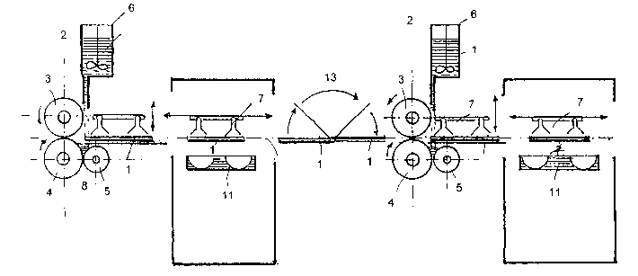
Figure 1 shows the apparatus of the present invention schematically.
Figure 2 shows a further embodiment of the apparatus according to the present
invention for the use
of powder coatings.
Figure 3 schematically shows a printed circuit board coated by a prior art
process.
Figure 4 shows a printed circuit board coated by the process according to the
present invention.
The reference signs used therein are denoting the following:
printed circuit board
(2) roll coating apparatus
(3) rubberised lead roll
(4) rubberised applicator roll
(5) metering roll
(6) storage container
(7) means to transport the printed
circuit boards
(8) coating knife
(9) metering roll
(10) copperconductor
( 11 ) means to transport the solder
stop lacquer
(12) screen case
4
CA 02502140 2005-04-12
Doc. No. 106-12 CA/PCT Patent
(13) turning device
( 14) coating of the edge areas of the conductor
Detailed Description of the Invention
In the following, the present invention is explained in more detail. The
application of the lacquer can
be carried out using processes known in the art, as long as the coating
apparatus used thereby has only
one coating unit to coat the bottom side of the substrates.
In case of using an apparatus according to claim 1 for example a solder stop
lacquer having a viscos-
ity of preferably 5000 to 15000 mPas at 25°C and a solids content of 50
to 100%, being both ther-
mally curable and curable by irradiation and containing preferably no or only
small amounts of min-
eral fillers is supplied to a first roll coating apparatus (2) together with a
printed circuit board (1) pro-
vided with conductors and drill holes to incorporate wired components, the
roll coating apparatus (2)
consisting of an upper rubberised guide roll (3), a lower rubberised
applicator roll (4) and a metering
roll (5) forming a metering gap together with the applicator roll (4). A wedge-
shaped coating knife (8)
can optionally be arranged between the applicator roll (4) and the metering
roll (5) for rendering the
edge areas of the printed circuit boards free of lacquer. A highly viscous
solder stop lacquer is me-
tered between the metering roll (5) and the applicator roll (4) from a storage
container (6) arranged
above the roll coating apparatus (2). The solder stop lacquer having a
viscosity of preferably 5000 to
15000 mPas is applied on the bottom side of the printed circuit board (1)
preferably at a speed of 1 to
4 m/min at a thickness of the layer of preferably 10 to 70 pm over the smooth
(Rz = 5 pm to 10 pm)
and supple (20 to 40 Shore A) rubber surface.
In the case of this highly viscous coating only a part of the lacquer layer
located on the applicator roll
is transferred due to the high adhesive strength of the lacquer on the rubber
coating. A requirement for
the transfer of the lacquer is the adhesive strength on the surface of the
printed circuit board to be
coated. Since this adhesive strength exhibits the highest values for the
copper conductors (10), the
thickest lacquer layer is consequently applied there. The drill holes are not
capable for forming an
adhesive area and therefore no lacquer is transferred there. According to
state of the art roll coating
processes, the lacquer is applied by means of a grooved rubber coating in such
a way that the lacquer
is pressed out of the grooves, whereby lacquer is also pressed into the drill
holes. In the process ac-
cording to the present invention the coating occurs independently from the
nature of surface to be
coated. Hence, the thus applied solder stop lacquer excellently covers the
conductors and maintains
the drill holes and the edge areas of the printed circuit boards free of
lacquer, so that a good soldering
of the wired components and a transport of the printed circuit board into the
drier is ensured. A dam-
5
CA 02502140 2005-04-12
Doc. No. 106-12 CA/PCT Patent
age of the rubber surface by cuts of the high conductors is prevented by the
rubber coating according
to the present invention in connection with the high viscosity of the coating.
After this coating, the printed circuit board (1) is transported via means to
transport the printed circuit
board (7), such as a chain transport means with transport clamps, into a
drier, such as an infrared
drier, which is only fitted under the transport paths with drying means, such
as an IR-irradiator ( 11 ).
These are equipped with irradiators in the medium wave length range of 2 to 4
pm. In contrast to the
heretofore used evaporation paths in a paternoster-type furnace, in which the
lacquer is to dry without
a reduction in viscosity, so that it does not run off the edge areas of the
conductor due to the reduction
in viscosity, the process according to the present invention aims at the
contrary effect. The viscosity
of the lacquer shall be reduced as fast as possible from its initial value of
5000 to 15000 mPas to be-
low 500 mPas. Hereby the before corrugated lacquer surface smoothes and the
lacquer flows up the
side walls of the conductor. The absence of mineral fillers favours this flow
process. The temperature
of the lacquer should be brought up to 100 to 120°C within 10 to 60
seconds. Dropping off is avoided
by the starting drying and the corresponding increase in viscosity. The drill
holes and the edge areas
remain free of lacquer. The subsequently starting drying results in a
hardening of the lacquer. After
being rendered non-tacky by drying and curing the printed circuit board (1) is
turned in a turning
means (13) and either coated for a second time using the same apparatus or
supplied to a second roll
coating apparatus constructed in the same way. As can be seen from Figure 3,
the conductors (14)
usually have a coating of the edges from 5 to 10 pm in case of a thickness of
the lacquer layer of
um. Using the process according to the present invention a coating of the
edges of the conductors
(14) of more than 10 ltm is achieved as illustrated in Figure 4.
According to the present invention, this is achieved by incorporating a
portion of a non-volatile sol-
25 vent with a boiling point of more than 120°C in an amount of 5 to 20
wt.-% and by the absence of
mineral fillers. In case of using a powdery solder stop lacquer, this is
achieved by reducing the viscos-
ity below 500 mPas. This absence of mineral fillers also enables a structuring
via laser without mush-
room-like residues of ash on the copper surfaces.
30 According to a further embodiment, the apparatus for carrying out the
process according to the pre-
sent invention exhibits a further metering roll (9). Between the metering
rolls (5) and (9) the highly
viscous solder stop lacquer is metered from a storage container (6) arranged
above the roll coating
apparatus (2). In case of using a thermally curable powdery solder stop
lacquer the lacquer is applied
via a screen case (12) onto the metering roll (5) rotating in opposite
direction compared to the applica-
for roll (4). The metering roll (5) absorbs the lacquer remaining on the
applicator roll (4) on which the
powdery solder stop lacquer is dispersed subsequently. Thus, an initial curing
is avoided and the roll
application of thermally curable powdery solder stop lacquers is enabled.
After adjusting the thickness
6
CA 02502140 2005-04-12
Doc. No. 106-12 CA/PCT Patent
of the layer by means of the metering rolls (5) and (9) the absence of lacquer
on the edges is achieved
by a film having a thickness of about 30-150 um which is stuck onto the fixed
metering roll (9), the
coating area being left free. Subsequently, this lacquer is transferred to the
smooth (Rz = 5-10 Vim)
and supple (20 to 40 Shore A) rubber surface of the applicator roll (4) by the
metering roll (5) running
in opposite direction and applied with a viscosity of preferably 5000 to 15000
mPas and with a speed
of 1 to 4 m/min in a thickness of the layer of 20 to 70 ~m onto the bottom
side of the printed circuit
board (1). In case of using a thermally curable, powdery solder stop lacquer
for the coating, each roll
and the printed circuit board to be coated is heated to a temperature with
which the required viscosity
of the coating is achieved.
The present invention is explained in more detail by the following examples:
Example 1:
Printed circuit board 300 x 420 x 1.5 mm Type FR 4 according to NEMA height of
the conductor
max. 100 ~m width of the conductor 150 ltm
Solder stop lacquer: Probimer 65 Fa. Vantico AG 100 parts by weight + 5 parts
by weight y-
butyrolacton
Roll coating apparatus: RC Fa. Biirkle rubber coating: 100 mm, 30 Shore A, Rz
5 ~m
Gap width: 100 ~m
Wet application: 50 ~m
Speed: 2 m/min
IR-irradiator: first irradiator having a wave length of 2 ltm, second
irradiator having a wave length of
4 ~m
Circulating air temperature: 120°C
Dryer length: 4 m
Result:
Thickness of the dry film: 30 ~m
Coating of the edge areas in case of a height of the conductor of 100 Vim: 11
~m
Drill holes diameter 300 to 1000 Vim: free of lacquer
7
CA 02502140 2005-04-12
Doc. No. 106-12 CA/PCT Patent
Example 2:
Printed circuit board (2) 300 x 420 x 1.5 mm Type FR 4 according to NEMA
height of the conductor
max. 100 ltm width of the conductor 150 pm
Solder stop lacquer (1): 125 parts by weight Rutapox VE 3746 80 wt.-% in
methylglycol, Fa. Bake-
lite AG
0.5 parts by weight 2-ethyl-4-methylimidazole, Fa. BASF
viscosity: 9500 mPas at 25°C
TG after curing for 1 hour at 160°C: 155°C
Roll coating apparatus: RC Fa. Biirkle, rubber coating: 100 mm, hardness: 30
Shore A, Rz 5 pm
Gap width: 100 pm
Wet application: 50 um
Speed: 2 m/min
IR-irradiator: first irradiator having a wave length of 2 ltm, second
irradiator having a wave length of
4 pm
Circulating air temperature: 120°C
Dryer length: 4 m
Curing at 160°C for 1 hour
Result coating:
Thickness of the dry film: 30 um
Coating of the edge area in case of a height of the conductor of 100 ltm: 11
ltm
Drill holes diameter 300 to 1000 ltm: free of lacquer
Result structuring via laser:
COZ laser: soldering pads free of ash residues
Result soldering:
Drill holes and soldering pads cleanly wetted with solder material
Example 3:
Printed circuit board 300 x 420 x 1.5 mm Type FR 4 according to NEMA height of
the conductor
max. 100 pm width of the conductor 100 pm
8
CA 02502140 2005-04-12
Doc. No. 106-12 CA/PCT Patent
Solder stop lacquer
80.0 parts by weight EPOSID VP 868-2, 70 wt.-% Duroplast-Chemie
19.5 parts by weight HAT 9490 Kresolnovolak 100 wt.-% Fa. Vantico
0.5 parts by weight 2-ethyl-4-methylimidazole Fa. BASF
100.0 parts by weight 75 wt.-
Viscosity: 7500 mPas at 25°C TG after curing for 1 hour at
160°C: 150°C
Roll coating apparatus: RC Fa. Robert Burkle GmbH Freudenstadt
Rubber coating: 100 mm
Hardness: 30 Shore A, Rz 5 um
Gap width: 120 pm
Wet application: 50 pm
Transferred amount: 42 vol.-
Speed: 2 m/min
IR-irradiator: first irradiator having a wave length of 2 pm, second
irradiator having a wave length of
4 um
Circulating air temperature: 120°C
Dryer length: 4 m
Result:
Thickness of the dry film: 30 pm
Coating of the edge area in case of a height of the conductor of 100 pm: 11 pm
Drill holes diameter 300 to 1000 pm: free of lacquer
Edge areas of the printed circuit board: 5 mm free of lacquer
Result structuring via laser:
COZ laser: soldering pads free of ash residues
Combustion gases: halogen-free
Result soldering:
Drill holes and soldering pads cleanly wetted with solder material
9
CA 02502140 2005-04-12
Doc. No. 106-12 CA/PCT Patent
Example 4:
Printed circuit board 300 x 420 x 1.5 mm Type FR 4 according to NEMA, height
of the conductor
max. 100 pm, width of the conductor 100 pm
Solder stop lacquer
80.0 parts by weight EPOSID VP 868-2, 70 wt.-%. Duroplast-Chemie
19.5 parts by weight HAT 9490 Kresolnovolak 100 wt.-% Fa. Vantico
0.5 parts by weight 2-ethyl-4-methylimidazole Fa. BASF
100.0 parts by weight 75 wt.-
Viscosity: 7500 m Pas at 25°C
Roll coating apparatus: RC Fa. Robert Burkle GmbH Freudenstadt
Rubber coating thickness: 100 mm
Hardness: 30 Shore A, Rz 5 ltm
Gap width between the metering rolls (5) and (9): 120 pm
Wet application: 50 pm
Transferred amount: 42 vol.-
Teflon film on the metering roll (9), open area at the right edge: 410 mm
Speed: 2 m/min
IR-irradiator: first irradiator having a wave length of 2 ltm, second
irradiator having a wave length of
4 ltm
Circulating air temperature: 120°C
Dryer length: 4 m
Example 5:
Printed circuit board 300 x 420 x 1.5 mm Type FR 4 according to NEMA height of
the conductor
max. 100 um width of the conductor 100 pm
Powdery solder stop lacquer:
95.00 parts by weight epoxy resin DER 671 Fa. Dow Chemical
4.5 parts by weight dicyandiamide
0.5 parts by weight 2-methylimidazole Fa. BASF
100.0 parts by weight powdery solder stop lacquer
CA 02502140 2005-04-12
Doc. No. 106-72 CA/PCT Patent
Melting region: 65-78°C
Viscosity: 14.00 m Pas at 110°C
Grain size: 10-20 ltm
TG after curing for 1 hour at 160°C: 160°C
Roll coating apparatus: H RC Fa. Robert Burkle GmbH Freudenstadt
Rubber coating: 10 mm
Hardness: 30 Shore A, Rz 5 ltm
Temperature of the applicator roll (4) and the metering rolls (5) and (9):
110°C
Temperature of the printed circuit board: 110°C
Teflon film on metering roll (9), open area at the right edge: 410 mm
Gap width between the metering roll (5) and (9): 50 ltm
Dry application: 30 um
Transferred amount: 60 vol.-
Speed: 3 m/min
IR-irradiator: first irradiator having a wave length of 2 ltm, second
irradiator having a wave length of
4 ltm
Circulating air temperature: 140°C
Dryer length: 4 m
Result:
First coating:
Thickness of the dry film: 30 ltm
Coating of the edge areas in case of a height of the conductor of 100 ltm: 11
ltm
Drill holes diameter 300 to 1000 ltm: free of lacquer
edges of the printed circuit board: S mm free of lacquer
Result:
Second coating:
Thickness of the dry film: 30 gm
Coating of the edge areas in case of a height of the conductor of 100 gm: 12
ltm
Drill holes diameter 300 to 1000 ltm: free of lacquer
Edges of the printed circuit boards: 5 mm free of lacquer
Result structuring via laser:
COz laser: soldering pads free of ash residues
Combustion gases: halogen-free
CA 02502140 2005-04-12
Doc. No. 106-12 CA/PCT Patent
Result soldering:
Drill holes and soldering pads cleanly wetted with soldering material
12