Language selection

Search

Patent 2503283 Summary

Third-party information liability

Some of the information on this Web page has been provided by external sources. The Government of Canada is not responsible for the accuracy, reliability or currency of the information supplied by external sources. Users wishing to rely upon this information should consult directly with the source of the information. Content provided by external sources is not subject to official languages, privacy and accessibility requirements.

Claims and Abstract availability

Any discrepancies in the text and image of the Claims and Abstract are due to differing posting times. Text of the Claims and Abstract are posted:

  • At the time the application is open to public inspection;
  • At the time of issue of the patent (grant).
(12) Patent Application: (11) CA 2503283
(54) English Title: METHOD FOR SCALED CURRENT PROGRAMMING OF AMOLED DISPLAYS
(54) French Title: METHODE DE PROGRAMMATION PAR COURANTS ECHELONNES POUR AFFICHEURS AMOLED
Status: Deemed Abandoned and Beyond the Period of Reinstatement - Pending Response to Notice of Disregarded Communication
Bibliographic Data
(51) International Patent Classification (IPC):
  • G09G 03/3225 (2016.01)
  • G09F 09/33 (2006.01)
(72) Inventors :
  • AROKIA, NATHAN (Canada)
  • REZA, CHAJI G. (Canada)
  • PEYMAN, SERVATI (Canada)
(73) Owners :
  • IGNIS INNOVATION INC.
(71) Applicants :
  • IGNIS INNOVATION INC. (Canada)
(74) Agent:
(74) Associate agent:
(45) Issued:
(22) Filed Date: 2005-04-08
(41) Open to Public Inspection: 2006-10-08
Availability of licence: N/A
Dedicated to the Public: N/A
(25) Language of filing: English

Patent Cooperation Treaty (PCT): No

(30) Application Priority Data: None

Abstracts

English Abstract


Disclosed is a technique for fast programming of the current cell and/or
current mirror circuits, in
particular current-programmed active matrix organic light emitting diode
(AMOLED) displays.


Claims

Note: Claims are shown in the official language in which they were submitted.
Sorry, the claims for patent document number 2503283 were not found.
Text is not available for all patent documents. The current dates of coverage are on the Currency of Information  page

Description

Note: Descriptions are shown in the official language in which they were submitted.


CA 02503283 2005-04-08
FIELD OF THE INVENTION
The present invention generally relates to a light emitting device displays,
and particularly, to a
driving technique for AMOLED. The present technique enhances the settling time
of the current-
programmed AMOLED displays.
BACKGROUND OF INVENTION
The small current required by the OLEDs coupled with a large parasitic
capacitance increases the
settling time of the programming of the current-programmed AMOLED displays.
More
importantly, design of external driver supplying that current is very
challenging and impractical.
For example, in the CMOS technology, the transistors must work in sub-
threshold regime to
provide the small current required by the OLEDs. Therefore, to use current-
programmed
AMOLED pixel circuits, suitable driving schemes are desirable.
Current scaling is one method that can be used to manage the challenges
associated with the
small current required by the OLEDs. In the current mirror pixel circuit, the
current scaling can
be done by resizing the mirror transistors. If the size of the drive
transistor is smaller than the size
of the other mirror transistor, the current passing through the OLED is scaled
down. However,
this method is not applicable for other current-programmed pixel circuits.
Also, by resizing the
two mirror transistors the effect of mismatch increases.
SUMMARY OF INVENTION
This invention provides a simple current programming technique, suitable for
the use in
AMOLED displays. Despite the other current scaling technique, resizing is not
required in the
new technique, resulting in a better matching between two mirror transistors
in the current-mirror
pixel circuits.

CA 02503283 2005-04-08
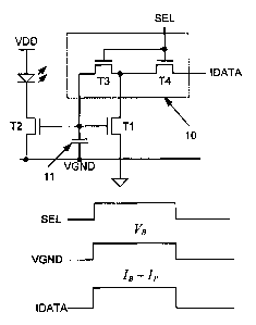
FIG. 1 current scaling in a current-mirror pixel circuit with virtual-ground
technique.

CA 02503283 2005-04-08
FIG. 1 shows a current-mirror pixel circuit with the new current scaling
technique as an example.
Here, T3, T4 are the switch network, 10. During the programming cycle T3 and
T4 are ON. A
current equal to (IB+IP) is passing through T3 and T4, and the gate-source
voltage of T1 is self
adjusted to ( Ip SIB + YT ) where VT is the threshold voltage of the drive
transistor, Tl. Here, IP
is the programming current, and IB the bias current. However, the voltage
stored in the storage
IP + IB - YB + YT . Since the source of T2 is connected to VGND, the
capacitance, 11, is VAS = ,
current flowing through the OLED during the programming time is
IP;Xer = IP + IB + ~.Yez - 2~ ~ VB ~ (IP + IB)
If IB » IP, we can rewrite the pixel current as
IP~er = Ir + (Ie +,(3.VB2 - 2~ ~ VB ~ IB )
By choosing VB properly (VB= ~ ), the pixel current becomes equal to the
programming
current (IP). Therefore, it avoids unwanted emission during the programming
cycle.
During the driving cycle, VGND is zero, so that the gate-source voltage of Tl
(T2) becomes
equal to Vas. Therefore, the current of the pixel is given by
Ipixel = Ip + IB + ~3.YB2 - 2~ ~ YB ~ (IP + IB) .
If IB » IP, we can rewrite the pixel current as
z
IP~er = Ir + (Ie +,Q.VB - 2~ ~ VB ~ Ia )
By choosing VB properly (VB= ~ ), the pixel current becomes equal to the
programming
current (IP).

Representative Drawing
A single figure which represents the drawing illustrating the invention.
Administrative Status

2024-08-01:As part of the Next Generation Patents (NGP) transition, the Canadian Patents Database (CPD) now contains a more detailed Event History, which replicates the Event Log of our new back-office solution.

Please note that "Inactive:" events refers to events no longer in use in our new back-office solution.

For a clearer understanding of the status of the application/patent presented on this page, the site Disclaimer , as well as the definitions for Patent , Event History , Maintenance Fee  and Payment History  should be consulted.

Event History

Description Date
Inactive: IPC deactivated 2016-01-16
Inactive: IPC assigned 2016-01-01
Inactive: First IPC assigned 2016-01-01
Inactive: First IPC assigned 2015-12-04
Inactive: IPC removed 2015-12-04
Inactive: IPC assigned 2015-12-04
Application Not Reinstated by Deadline 2007-07-11
Inactive: Dead - No reply to Office letter 2007-07-11
Deemed Abandoned - Failure to Respond to Maintenance Fee Notice 2007-04-10
Deemed Abandoned - Failure to Respond to Notice Requiring a Translation 2007-04-10
Inactive: Office letter 2007-03-14
Inactive: Entity size changed 2007-03-14
Inactive: Corrective payment - s.78.6 Act 2007-01-31
Inactive: Incomplete 2007-01-09
Inactive: Status info is complete as of Log entry date 2006-10-19
Inactive: Cover page published 2006-10-08
Application Published (Open to Public Inspection) 2006-10-08
Inactive: Abandoned - No reply to Office letter 2006-07-11
Inactive: IPC assigned 2005-05-25
Inactive: First IPC assigned 2005-05-25
Inactive: Filing certificate - No RFE (English) 2005-05-10
Application Received - Regular National 2005-05-10

Abandonment History

Abandonment Date Reason Reinstatement Date
2007-04-10
2007-04-10

Fee History

Fee Type Anniversary Year Due Date Paid Date
Application fee - small 2005-04-08
2007-01-31
Owners on Record

Note: Records showing the ownership history in alphabetical order.

Current Owners on Record
IGNIS INNOVATION INC.
Past Owners on Record
CHAJI G. REZA
NATHAN AROKIA
SERVATI PEYMAN
Past Owners that do not appear in the "Owners on Record" listing will appear in other documentation within the application.
Documents

To view selected files, please enter reCAPTCHA code :


To view images, click a link in the Document Description column. To download the documents, select one or more checkboxes in the first column and then click the "Download Selected in PDF format (Zip Archive)" or the "Download Selected as Single PDF" button.

List of published and non-published patent-specific documents on the CPD .

If you have any difficulty accessing content, you can call the Client Service Centre at 1-866-997-1936 or send them an e-mail at CIPO Client Service Centre.


Document
Description 
Date
(yyyy-mm-dd) 
Number of pages   Size of Image (KB) 
Claims 2006-10-07 1 2
Abstract 2005-04-07 1 7
Description 2005-04-07 3 74
Drawings 2005-04-07 1 7
Representative drawing 2006-01-23 1 4
Filing Certificate (English) 2005-05-09 1 157
Request for evidence or missing transfer 2006-04-10 1 103
Courtesy - Abandonment Letter (Office letter) 2006-08-21 1 166
Notice: Maintenance Fee Reminder 2007-01-08 1 126
Courtesy - Abandonment Letter (incomplete) 2007-04-30 1 166
Courtesy - Abandonment Letter (Maintenance Fee) 2007-06-04 1 176
Correspondence 2005-05-09 1 38
Correspondence 2007-01-03 1 19
Correspondence 2007-03-13 1 13