Note: Descriptions are shown in the official language in which they were submitted.
CA 02503501 2005-04-22
SPECIFICATION
OPTICAL SIGNAL AMPLIFYING TRIODE AND OPTICAL SIGNAL TRANSFER
METHOD, OPTICAL SIGNAL RELAY DEVICE, AND OPTICAL SIGNAL STORAGE
DEVICE USING THE SAME
[0001]
Technical Field
This invention concerns (a) an optical signal amplifying triode
that amplifies, controls, orswitchesopticalsignals, particularly
an optical signal amplifier favorable for optical communication,
optical image processing, optical computers, optical measurements,
optical integrated circuits and other optoelectronic applications
enabling advanced information processing, (b) an optical signal
transfer method and an optical signal relay device for transferring
optical signals, which have been propagated via an optical fiber
or other predetermined transmission path, to other transmission
paths indicated by routing information included in the optical
signals, and (c) an optical signal storage device that stores optical
signals, which have been propagated via an optical fiber or other
predetermined transmission path, and enables the optical signals
to be taken out at any arbitrary time.
[0002]
Background Art
Wide deployment of moving image communication, video
distribution, and other new broadband services, using opticalfiber
communication that enables broadband and high-speed transmission,
is anticipated. However, a functional (signal amplification)
element, which, for example, corresponds to a triode transistor
1
CA 02503501 2005-04-22
in electronics, that is, an optical functional element that performs
signal amplification of optical signals by direct control by other
optical signals has not been realized as of yet.
[0003]
Thus presently, optical signals that have been transmitted
at high speed are converted once into electrical signals, which
are then subject to information processing in an electronic circuit,
and the processed signals are converted back into and transmitted
as optical signals. A limit is thus placed in the speed of signal
processing due to the inability to directly control light by light .
It is said that if signal processing can be performed on optical
signals as they are, parallel processing will be enabled and further
shortening of the processing time can be anticipated.
[0004]
In this regard, the devices described in Document 1 or Document
2 are simply devices that switch light, in other words, gate switching
devices that make use of wavelength conversion by Mach-Zehnder
optical interferometry, and these devices had problems of being
weak against temperature change and vibration and being strict in
terms of setting conditions. Such conventional arts do not disclose
anything in regard to arranging an optical signal amplifying triode,
which, like a transistor in an electronic circuit, is equipped with
a function of using input light as control light to obtain
signal-amplified output light.
[0005]
In the field of optical communication enabling broadband,
high-speed,and high-capacitysignaltransmission,itisanticipated
that communication, transfer, and distribution of optical signals
be performed without degradation of the properties of high speed
2
CA 02503501 2005-04-22
and high capacity. For an optical network based on wavelength
division multiplexing (WDM), which is predicted to be constructed
in the relatively near future, an optical signal transfer (optical
signal relaying) art, of transferring wavelength division
multiplexed optical signals, which are a plurality of types of laser
light differing in wavelength and which have been transmitted from
one opticaltransmission path,to desired opticaltransmission paths
according to wavelength, will be important. In optical signal
transfer for transferring an optical signal train (for example,
a packet signal) that has been propagated via an optical fiber or
other predetermined transmission path (for example, a wavelength
bus) to other transmission paths indicated by labels, tags, or other
routing information attached to the optical signal train, that is
for example, in routing within an optical network or among optical
networks, the high-capacity and high-speed characteristics of
optical signal transmission must not be degraded and routers, that
is, optical signal relay (transfer) devices are required to perform
transfer processes at high-speed, be high in reliability, and be
compact.
[0006]
An optical path cross-connection device, such as that described
in Document 3, has been proposed for this purpose. This device is
equipped with a wavelength splitter, which splits a wavelength bus
for wavelength multiplex transmission link into N wavelength group
buses of G wavelengths each, and a routing processor, which executes
a routing process on each of the wavelength groups split by the
wavelength splitter, and is thus arranged to perform the routing
process according to wavelength group. The routing processor of
this optical path cross-connection device comprises a wavelength
3
CA 02503501 2005-04-22
converter, which performs wavelength conversion according to each
wavelength group, and an optical matrix switch, which distributes
the wavelength-converted light and is controlled by a controller.
This optical matrix switch is arranged with a mechanically-operated
reflecting mirror switch that is positioned at the intersection
of matrix-like optical paths and is alternatively operated by the
controller to make one wavelength group, among the plurality of
wavelength groups, be reflected by the reflecting mirror switch
and thereby be output to a desired transmission path (paragraph
0042, Fig. 10 (1) ) , or has an optical switch, which is alternatively
operated by the controller, and mesh wiring and is arranged to make
one wavelength group, among the plurality of wavelength groups,
be transmitted by the optical switch and thereby be output to one
transmission path inside the mesh wiring (paragraph 0043, Fig.
10(2)).
[0007]
However, with the above-described conventional optical path
cross-connection device, since the routing process is performed
by the reflecting mirror switch or the optical switch, the operation
of which is controlled by the controller, the switching operation
of the reflecting mirror switch or the optical switch is performed
in accordance with a command signal, which indicates the routing
destination (destination) and is an output that is electronically
processed at the controller. A portion of the optical signal thus
had to be converted to an electrical signal, the destination
information contained in the electrical signal, that is, a
transfer-related signal included in a label or tag of a packet had
to be extracted, and the optical signal had to transferred upon
electrically controlling the operation of the reflecting mirror
4
CA 02503501 2005-04-22
switch or the optical switch in accordance with the transfer-related
signal. Thus, an adequate response speed could not be obtained.
Also besides the above-described routing processor, since a
wavelength converter, for performing wavelength conversion in
accordance with the wavelength of the transmission path (wavelength
bus) of the transfer destination, is equipped, and such a wavelength
converter is disposed in addition to the routing processor, the
device became large and in some cases, especially when a mechanically
operated reflecting mirror switch is used, reliability could not
be obtained.
[0008]
Furthermore, in the field of optical communication enabling
broadband, high-speed, and high-capacity signal transmission, it
isanticipatedthat theidentification, multiplexing andsplitting,
switching, and routing (transfer, distribution) of optical signals
(optical data, such as packet signals ) be performed without degrading
the characteristics of broadband, high speed, and high capacity.
In this field of optics, optical signal storage devices, which enable
temporary storage and take-out at desired timings of optical signals,
are generally demanded for optical signal processing systems that
process optical signals and are represented, for example, by photonic
router systems. This is because, just as memories are essential
in signal processing in the field of electronics, optical signal
storage devices, referred to as optical memories or optical buffers,
are essential in the field of optical signal processing.
[0009]
In this regard, optical memory devices, such as that described
in Patent Document 1, have been proposed. With this device, a
plurality of optical waveguide means 105 to 108, respectively
CA 02503501 2005-04-22
arranged from optical fibers of different length in order to provide
a plurality of types of delay times, are prepared, and arrangements
to pass an optical signal through any of optical waveguide means
105 to 108 and enable storage of the optical signal by just the
delay time corresponding to the propagation time in the corresponding
optical waveguide means among optical waveguide means 105 to 108.
[0010]
However, with this conventional optical memory device, the
storage time of an optical signal is only determined in advance
by the delay time corresponding to the propagation time in the optical
waveguide means among optical waveguide means 105 to 108 through
which the optical signal is made to propagate and the optical signal
thus cannot be taken out at a desired timing. The degree of freedom
of optical signal processing was thus limited and lowering of signal
processing efficiency could not be avoided.
[0011]
[Document 1] K. E. Stubkjaer, "Semiconductor optical
amplifier-based all-optical gates for high-speed optical
processing, " IEEE J. Quantum Electron. , vol . 6, no. 6, pp. 1428-1435,
Nov./Dec. 2000.
[Document 2] T. Durhuus, C. Joergensen, B. Mikkelsen, R. J.
S. Pedersen, and A. E. Stubkjaer, "All optical wavelength conversion
by SOAs in a Mach-Zehnder configuration," IEEE Photon. Technol.
Lett., vol. 6, pp. 53-55, Jan. 1994.
[Document 3] Japanese Published Unexamined Patent
Application No. 2002-262319
[Document 4] Japanese Published Unexamined Patent
Application No. Hei 8-204718
[0012]
6
CA 02503501 2005-04-22
This invention has been made with the above circumstances as
a background, and a first object thereof is to provide an optical
signal amplifying triode that can perform an amplification process
directly on optical signals by using control light. A second object
is to provide an optical signal transfer method and an optical signal
relay device, with which the routing of optical signals can be
processed at high speed or by a compact device. A third object is
to provide an optical signal storage device that enables storage
of optical signals and taking out of the optical signals at an
arbitrary time.
[0013]
Upon carrying out various examinations with the above
circumstances as the background, the present inventor found that
in an optical amplifier, such as a semiconductor optical amplifier,
a rare-earth-element-doped fiber amp, etc., spontaneously emitted
light of peripheral wavelengths of an input light of a predetermined
wavelength 1~1 vary in intensity in response to intensity variations
of the input light and this ix~tensity variation varies inversely
with respect to that of the signal intensity variation of the input
light, and found a laser-induced signal enhancement effect, that
is, a phenomenon wherein when laser light of another wavelength
1~2 within the wavelength range of the spontaneously emitted light,
that is, within the peripheral wavelength range of the input light
is made incident upon being multiplexed with the input light, the
overall intensity increases suddenly, with the signal (amplitude)
variation of the spontaneously emitted light being maintained. The
present inventor grasped this phenomenon as a wavelength conversion
function from wavelength 1~1 to 1~2 and conceived an optical triode
based on a tandem wavelength converter (All-Optical Triode Based
CA 02503501 2005-04-22
on Tandem Wavelength Converter), with which this wavelength
conversion is connected in two stages, and thus came to conceive
an optical signal amplifying triode. Afirst aspect of this invention
was made based on this knowledge.
[0014]
The present inventor also noted that the optical amplifier
of the above-mentioned optical signal amplifying triode not only
has the function of wavelength conversion from wavelength hl to Az
but is also a functional element equipped with the wavelength
conversion function and a switching function and found that, by
multiplexing optical signals with routing information by amplitude
modulation, the functional element can be used favorably as a routing
device, that is, a transfer device for wavelength multiplexed signals .
A second and a third aspect of this invention was made based on
this knowledge.
[0015]
The present inventor also found that by making an optical
amplifier of an optical signal amplifying triode, which exhibits
the above-described phenomenon, perform the function of wavelength
conversion from wavelength 1~1 to 1~2 and at the same time combining
this optical amplifier with a wavelength splatter that performs
distribution to different output transmission paths in accordance
with the input wavelengths and interposing this combination in a
ring transmission path in which optical signals circulate, the
optical signals that are stored by being made to circulate can be
taken out at an arbitrary timing. A fourth aspect of this invention
was made based on this knowledge.
[0016]
Disclosure of the Invention
s
CA 02503501 2005-04-22
First Aspect of the Invention
This aspect of the invention provides an optical signal
amplifying triode comprising (a) a first semiconductor optical
amplifier and a second semiconductor optical amplifier, each
equipping an active layer formed of a pn junction and amplifying,
performing wavelength conversion on, and then outputting an optical
signal input therein; (b) a first optical input means, inputting
a first input light of a first wavelength and a second input light
of a second wavelength into the first semiconductor optical
amplifier; (c) a first wavelength selector, selecting light of the
second wavelength from among the light from the first semiconductor
optical amplifier; (d) a second optical input means, inputting the
light of second wavelength that has been selected by the first
wavelength selector and a third input light of a third wavelength
into the second semiconductor optical amplifier; and (e) a second
wavelength selector, selecting output light of the third wavelength
from among the light from the second semiconductor optical amplifier;
( f ) wherein the output light of the third wavelength is modulated
in response to the intensity variation of either or both of the
first input light of the first wavelength and the third input light
of the third wavelength and the signal gain with respect to the
third input light of the third wavelength is 2 or more.
[0017]
With this arrangement, when the light of the second wavelength,
selected from the light from the first semiconductor optical
amplifier into which the first input light of the first wavelength
and the second input light of the second wavelength have been input,
and the third input light of the third wavelength are input into
the second semiconductor optical amplifier, the output light of
9
CA 02503501 2005-04-22
the third wavelength, selected from the light emitted from the second
semiconductor optical amplifier, is light that is modulated in
response to the intensity variation of either or both of the
above-mentioned first input light of the first wavelength and the
third input light of the third wavelength and is an amplified signal
with a signal gain of a magnitude of 2 or more with respect to the
above-mentioned third input light of the third wavelength. An
opticalsignalamplifyingtriode, which can perform anamplification
process directly on optical signals by using control input light,
can thus be provided. Also, since each of the first semiconductor
optical amplifier and the second semiconductor optical amplifier
is an optical amplifier equipped with an active layer comprising
a pn junction, the optical signal amplifying triode is made compact
and higher in signal gain.
[0018]
Preferably, this aspect of the invention provides the optical
signal amplifying triode, wherein the first input light of the first
wavelength is modulated light, the second input light of the second
wavelength is continuous light, the third input light of the third
wavelength is control light, and the output light of the third
wavelength has a signal waveform, with which the modulation signal
of the first input light is amplified, in the input interval of
the control light. In this case, the output light of the third
wavelength will be amplified light that has been modulated in response
to the intensity variation of the first input light of the first
wavelength in the input interval of the control light . An optical
signal amplifying triode, which can perform a switching process
directly on amplified optical signals by using control input light,
can thus be provided.
io
CA 02503501 2005-04-22
[0019]
Preferably, this aspect of the invention provides the optical
signal amplifying triode, wherein the third wavelength is the same
as the first wavelength. In this case, since the first input light
and the third input light, which are the signal input light of the
optical signal amplifying triode, and the output light will be of
the same wavelength, connection of a plurality of the optical signal
amplifying triodes with a common wavelength is enabled and an optical
circuit of a high degree of integration can be arranged using the
plurality of the optical signal amplifying triodes.
[0020]
Preferably, this aspect of the invention provides the optical
signal amplifying triode, wherein the signal gain of the output
light of the third wavelength with respect to the control light
of the third wavelength is 10 or more. The signal gain of the optical
signal amplifying triode can then be increased further.
[0021]
Preferably, this aspect of the invention provides the optical
signal amplifying triode, wherein the active layers of the
semiconductor optical amplifiers are arranged from quantum wells,
a strained-layer superlattiCe, or quantum dots. Since a
semiconductor optical amplifier, equipped with an active layer
comprising quantum wells or quantum dots, is thus used, high-speed
response is enabled. Especially in the case where quantum dots are
used, a response speed of 100GHz or more can be obtained. Also,
polarization dependence is lessened by the use of a strained-layer
superlattice.
[0022]
Preferably, this aspect of the invention provides the optical
11
CA 02503501 2005-04-22
signal amplifying triode, further comprising a reflecting means,
reflecting light that has been transmitted through the active layer
of an above-mentioned semiconductor optical amplifier towards the
semiconductor optical amplifier or the other semiconductor optical
amplifier. Since the transmission path in the active layer will
then be elongated practically by the reflecting means equipped at
one end face, the signal gain can be increased further. The
modulation degree of the output signal is also increased further
by the feedback effect.
[0023]
Preferably, this aspect of the invention provides the optical
signal amplifying triode, wherein either or each of the first
semiconductor optical amplifier and second semiconductor optical
amplifier is equipped at one face thereof with a reflecting means
that selectively reflects light, and the reflection means is
optically coupled via a lens to either or each of the first
semiconductor optical amplifier and second semiconductor optical
amplifier. Here, a microlens can be used favorably as a converging
lens and the input light and the output light are transmitted via
optical fibers.
[0024]
Preferably, this aspect of the invention provides the optical
signal amplifying triode, wherein the reflecting means comprises
a first wavelength selective mirror, which, among the light from
the first semiconductor optical amplifier, does not reflect the
first input light of the first wavelength but reflects light of
thesecond wavelength to thesecondsemiconductoropticalamplifier;
and a second wavelength selective mirror, which, among the light
from the second semiconductor optical amplifier, does not reflect
12
CA 02503501 2005-04-22
the second input light of the first wavelength but reflects light
of the third wavelength. In this case, the reflecting means is
arranged from the wavelength selective mirror that functions as
the first wavelength selector and the wavelength selective mirror
that functions as the second wavelength selector.
[0025]
Preferably, this aspect of the invention provides the optical
signal amplifying triode, wherein a wavelength selective filter,
which does not transmit light of the first wavelength but transmits
light of the second wavelength, is disposed between one end face
of the first semiconductor optical amplifier and the reflecting
means for reflecting light, and a wavelength selective filter, which
does not transmit light of the second wavelength but transmits the
wavelength of the control light, is disposed between one end face
of the second semiconductor optical amplifier and the reflecting
means for reflecting light. In this case, the first wavelength
selector and the second wavelength selector are arranged from the
first wavelength selection filter and the second wavelength
selection filter. Also, since the first input light, that is, light
of the first wavelength, which is the wavelength of the signal light,
is not transmitted by the first wavelength selection filter, even
better characteristics are provided.
[0026]
Preferably, this aspect of the invention provides the optical
signal amplifying triode, wherein the reflecting means functions
as either or both of the first wavelength selector and second
wavelength selector and the output light from an above-mentioned
semiconductor optical amplifier is input into the other
semiconductor optical amplifier by changing one or both of the
13
CA 02503501 2005-04-22
incidence angle of the input light and the emission angle of the
output light with respect to the reflecting means.
[0027]
Preferably, this aspect of the invention provides the optical
signal amplifying triode, wherein a plurality of sets of the first
semiconductor optical amplifier and second semiconductor optical
amplifier are disposed in optical waveguides formed on a
semiconductor substrate and these sets are integrated as a single
chip. In this case, the optical signal amplifying triode can be
made to have the smaller monolithic structure of a single integrated
chip.
[ooza]
Preferably, this aspect of the invention provides the optical
signal amplifying triode, further comprising an optical circulator
or a directional coupler, which makes input light be input into
an above-mentioned semiconductor optical amplifier through one end
face of the semiconductor optical amplifier and guides light, output
from the semiconductor optical amplifier through the one end face,
to an optical path that differs from that of the input light. In
this case, light that exits from the other end face of the
semiconductor amplifier will not enter a waveguide, which guides
light that is to be made incident on the other end face, but will
mainly be guided to another output waveguide.
[0029)
Preferably, this aspect of the invention provides the optical
signal amplifying triode, wherein a wavelength selective mirror
or wavelength selective filter that functions as the first wavelength
selector or second wavelength selector is disposed inside an optical
path and is arranged from any among the group consisting of a grating
14
CA 02503501 2005-04-22
filter, with which the refractive index is varied periodically in
the light propagation direction, a multilayer film filter, formed
by layering a plurality of sets of layers that differ in refractive
index, and a photonic crystal, having a photonic bandgap. In this
case, the second wavelength or the third wavelength is extracted
favorably from the light from the first semiconductor optical
amplifier or the second semiconductor optical amplifier.
[0030]
Preferably, this aspect of the invention provides the optical
signal amplifying triode, wherein the optical signal amplifying
triode makes up an optical HAND gate, an optical NOR gate, an optical
flip-flop circuit, or an optical operational amplifier. In this
case, an optical digital circuit or an optical analog circuit can
be arranged favorably from the above-described optical signal
amplifying triode.
[0031]
Also, with the above-described optical signal amplifying
triode, components, such as the first semiconductor optical
amplifier, the second semiconductor optical amplifier, the first
wavelength selector, the second wavelength selector, an optical
coupler, which multiplexes light to be input into the above components,
etc., may be coupled by means of optical waveguides formed on a
semiconductor substrate or a substrate formed of a light transmitting
substance, such as a glass substrate.
[0032]
Second Aspect of the Invention
This aspect of the invention provides an optical signal transfer
method of transferring an optical signal train, which has been
transmitted via a predetermined transmission path, to transmission
CA 02503501 2005-04-22
paths, among a plurality of transmission paths, that correspond
to routing information contained in the optical signal, the optical
signal transfer method comprising: (a) an input step of inputting
the optical signal train, to which the routing information have
been applied, to the main optical signal amplifying triode unit;
(b) a wavelength conversion step of supplying control light of
wavelengths, corresponding to signals indicating the routing
information, to the main optical signal amplifying triode unit,
and making optical signals of the wavelengths of the control light
be output from the main optical signal amplifying triode unit; and
(c) an optical distribution step of inputting the optical signals,
output from the main optical signal amplifying triode unit, into
an optical distributor and distributing the optical signals
according to their wavelengths among the plurality of optical
transmission pathsconnected to the opticaldistributor. Amplitude
modulation signals are thus added to the optical signal train as
the routing information and the optical signal train is thereby
arranged to be transferred to the destinations indicated by the
amplitude modulation signals.
[0033)
With this arrangement, the optical signal train, to which the
routing information have been provided, is input into the main optical
signal amplifying triode unit, the control light of the wavelengths
corresponding to the amplitude modulation signals are supplied to
the main optical signal amplifying triode unit, optical signals
of the wavelengths of the control light are output to the optical
distributor from the main optical signal amplifying triode unit,
and routing is carried out by the output optical signals being
distributed according to their wavelengths among the plurality of
16
CA 02503501 2005-04-22
optical transmission paths connected to the optical distributor.
Since the routing information are thus added to the optical signals,
the main optical signal amplifying triode unit, having a wavelength
conversion function and a switching function, can output optical
signals of wavelengths corresponding to the routing information
and these signals can then be distributed by the optical distributor.
A routing device, that is, an optical signal transfer device or
optical signal relay device of high speed and compact size can thus
be realized.
[0034]
Here, the routing information are information, such as IP
addresses, source addresses, destination addresses, source routing
and other route information, data link layer connection information,
etc., which are related to the determination of the transfer
destinations of optical signals.
[0035]
Preferably, this aspect of the invention provides the optical
signal transfer method, wherein the optical signal train is amplitude
modulated at a modulation degree of no more than 90 0 . In this case,
optical signals will not be degraded and the routing information
will be added securely to the optical signals.
[0036]
Preferably, this aspect of the invention provides the optical
signal transfer method, wherein the optical signal train is a packet
signal and the routing information are label information or tag
information provided at a head portion of the packet signal. Also
preferably, the above-mentioned optical signal train is a packet
signal and the above-mentioned routing information are label
information or tag information provided at a head portion of the
17
CA 02503501 2005-04-22
packet signal. Label information or tag information can thus be
added by amplitude modulation to a label portion or tag portion
provided at the head portion of the optical signal train that makes
up the packet signal.
[0037)
Preferably, this aspect of the invention provides the optical
signal transfer method, wherein in the wavelength conversion step,
amplitude modulation using the control light is applied to the optical
signals, output from the main optical signal amplifying triode unit,
to add new routing information to the optical signals . In this case,
the transfer destinations can be added as suited inside a transfer
device. Dynamic routing, by which the transfer route is determined,
for example, according to the link state, node state, and traffic
state, is thus enabled.
[0038]
Third Aspect of the Invention
This aspect of the invention provides an optical signal relay
device, which,among opticalsignaltransmission networks,transfers
an optical signal train, having routing information added thereto
by amplitude modulation, from one network to transmission paths,
among the transmission paths of another network, that correspond
to the routing information contained in the optical signal,
comprising: (a) a control light generator, generating, based on
the amplitudemodulation signals of the optical signal train, control
light of wavelengths corresponding to the destinations indicated
by the amplitude modulation signals; (b) a main optical signal
amplifying triode unit, converting the optical signal train into
an optical signal of the wavelengths of the control light; and (c)
an optical distributor, distributing the optical signal, output
1a
CA 02503501 2005-04-22
from the main optical signal amplifying triode unit, among a plurality
of optical transmission paths in accordance with the wavelengths
of the optical signal.
[0039]
With this arrangement, when an optical signal train, having
amplitude modulation signals added as routing information, arrives
upon being transmitted, control light of wavelengths corresponding
to the destinations indicated by the amplitude modulation signals
are generated by the control light generator based on the amplitude
modulation signals of the optical signal train, the optical signal
train is converted into optical signals of the wavelengths of the
above-mentioned control light bythe main optical signal amplifying
triode unit, and the optical signals output from the main optical
signal amplifying triode unit are distributed among the plurality
of optical transmission paths in accordance with their wavelengths
bytheopticaldistributor. Sincethe main opticalsignalamplifying
triode unit, having a wavelength conversion function and a switching
function, can thus output optical signals of wavelengths
corresponding to the routing information and these signals can then
be distributed by the optical distributor, a routing device, that
is, an optical signal transfer device or optical signal relay device
of high speed and compact size can be realized.
[0040]
Preferably, this aspect of the invention provides the optical
signal relay device, further comprising an electronic controller
or an all-optical controller, which, in accordance with the amplitude
modulation signals contained in the optical signal, makes control
light of wavelengths, which are in accordance with the routing
information indicated by the amplitude modulation signals, be
19
CA 02503501 2005-04-22
generated from the control light generator. In this case, since
the control light generator is controlled by the electronic
controller or the all-optical controller to generate the control
light of the wavelengths that are in accordance with the routing
informationindicated bythe amplitudemodulationsignals contained
in the optical signals, the main optical signal amplifying triode
unit, having a wavelength conversion function and a switching
function, can output optical signals of wavelengths corresponding
to the routing information and these signals can then be distributed
by the optical distributor. A routing device, that is, an optical
signal transfer device or optical signal relay device of high speed
and compact size can thus be realized. Also in the case where the
electronic controller is an all-optical controller that optically
extracts just the amplitude modulation signals contained in the
optical signals input from the above-mentioned main optical
waveguide and makes control light of wavelengths corresponding to
the address signals be generated from the control light generator,
the merit that the confidentiality of the optical signals can be
secured is provided since electromagnetic waves corresponding to
signals besides the address signals are not generated.
[0041]
Preferably, this aspect of the invention provides the optical
signal relay device, further comprising: (a) an optical splitter,
branching a portion of the optical signal; (b) a photoelectrical
signal converter, converting the optical signal branched by the
optical sputter to an electrical signal and supplying the electrical
signal to the electronic controller; and ( c) an optical delay element,
disposed at the downstream side of the optical splitter and delaying
the optical signal that is to be input into the main optical signal
CA 02503501 2005-04-22
amplifying triode unit upon passage through optical splitter; and
whereintheelectronic controllerextractsthe amplitude modulation
signals contained in the optical signal and makes control light
of wavelengths, which are in accordance with the routing information
indicated by the amplitude modulation signals, be generated from
the control light generator. Since the main optical signal
amplifying triode unit, having a wavelength conversion function
and a switching function, can thus output optical signals of
wavelengths corresponding to the routing information and these
signals can then be distributed by the optical distributor, a routing
device, that is, an optical signal transfer device or optical signal
relay device of high speed and compact size can be realized.
[0042]
Preferably, this aspect of the invention provides the optical
signal relay device, further comprising: an optical signal storage
element,temporarilystoring an opticaldistributedfromthe optical
signal distributor; and an optical feedback transmission path,
feeding back the optical signal output from the optical signal storage
element to the input side; and wherein when the optical signal is
an optical packet signal that is to be stored temporarily, the
electronic controller makesacontrolopticalsignal,forconverting
the optical packet signal to a priorly set storage wavelength, be
output, and the optical distributor distributes the optical packet
signal, after conversion to the storage wavelength, to the optical
signal storage element and makes the optical packet signal be stored
temporarily in the optical signal storage element. Here, a merit
is provided in that when a plurality of optical packet signals that
are subject to relay processing are to be output to the same
transmission path, one of the optical packet signals is converted
21
CA 02503501 2005-04-22
to the priorly set storage wavelength, the optical wavelength
sputter distributes the optical packet signal after conversion
to the storage wavelength to the above-mentioned optical signal
storage element, and after being stored in the storage element
temporarily, the optical packet signal is returned to the input
side and subject anew to the relay process.
[0043] '
Preferably, this aspect of the invention provides the optical
signal relay device, wherein the optical signal storage element
is equipped with a plurality of optical fibers, which are disposed
in parallel and differ in optical propagation length in order to
receive optical signals distributed by the optical distribution
device, the electronic controller makes a control optical signal,
for converting the optical packet signal to be stored temporarily
to a priorly set storage wavelength in accordance with the storage
time required of the optical packet signal, be output, and the optical
distributordistributesthe opticalpacket signal, afterconversion
to the storage wavelength, to an optical fiber among the plurality
of optical fibers of the optical signal storage element and
temporarily stores the optical packet signal in the optical fiber.
In this case, an optical packet signal is temporarily stored in
the process of being propagated inside an optical fiber, which,
among the plurality of optical fibers disposed in parallel, is in
accordance with the storage time required of the optical packet
signal.
[0044]
Preferably, this aspect of the invention provides the optical
signal relay device, wherein the all-optical controller comprises:
an optical coupler, branching a portion of the f first input light;
22
CA 02503501 2005-04-22
a continuous light source, generating continuous light of the same
wavelengths as the control light; an optical coupler, multiplexing
the continuous light from the continuous light source with the portion
of the first input light from the optical coupler; and a semiconductor
optical amplifier, receiving the light from the optical coupler,
outputting control light having the modulation signals contained
in the first input light, and being of slower response speed than
the semiconductor optical amplifier. A controller can thus be
arranged in an all-optical manner.
[0045]
Preferably, this aspect of the invention provides the optical
signal relay device, wherein when output light that are from the
main optical signal amplifying triode unit are input, the optical
distributor selectively distributes the output light, which have
been input, to optical transmission paths, among the plurality of
optical transmission paths, that correspond to the wavelengths of
the control light. For example, the optical distributor is an array
waveguide grating type wavelength splitter equipped with a first
slab waveguide, connected to an input port, a second slab waveguide,
connected to a plurality of output ports, and a plurality of array
waveguides of different lengths, disposed between the first slab
waveguide and the second slab wave guide, and distributes the input
light, input into the input port, among the plurality of output
ports according to the wavelengths of the input light. Such
arrangements include a diffraction grating type or prism type optical
distributor, which uses the refraction angles of a diffraction
grating or a prism that differ according to wavelength to selectively
distribute input light among a plurality of array waveguides aligned
in array form. With such an arrangement, an output light, which
23
CA 02503501 2005-04-22
is output from the above-described optical triode and is of a
wavelength corresponding to the control light, is distributed
selectively according to wavelength to one of the plurality of branch
waveguides.
[0046]
Fourth Aspect of the Invention
This aspect of the invention provides an optical signal storage
device, storing an optical signal input from an input optical
transmission path and enabling taking out of the optical signal
at an arbitrary time, comprising: (a) a control light generator,
generating control light for converting the optical signal input
from the input optical transmission path to wavelengths, which
correspond to the transmission destinations contained in the input
signal and are the same as or different from that of the optical
signal; (b) a main optical signal amplifying triode unit, receiving
the optical signal that has been input and the control light and
converting the optical signal that has been input to optical signals
of the wavelengths of the control light; (c) an optical distributor,
distributing the optical signals, output from the main optical signal
amplifying triode unit, in accordance with the wavelengths of the
optical signals; (d) an optical buffer memory element, temporarily
storing an optical signal of a storage wavelength that has been
distributed by the optical distributor; (e) an optical feedback
transmission path, feeding back the optical signal output from the
optical buffer memory element to the input optical transmission
path to re-input the optical signal into the main optical signal
amplifying triode unit; and (f) an optical signal storage control
means, making the control light generator output control light for
conversion of the optical signal, which is repeatedly circulated
24
CA 02503501 2005-04-22
through the main optical signal amplifying triode unit, optical
distributor,opticalbuffer memory element,andthe opticalfeedback
transmission path, to an output wavelength at the main optical signal
amplifying triode unit.
[0047]
With this fourth aspect of this invention, when the optical
signal, which is made to circulate repeatedly through the
above-mentioned main opticalsignalamplifying triode unit, optical
distributor, optical buffer memory element, and optical feedback
transmission path, is converted to the output wavelength in the
main optical signal amplifying triode unit by the optical signal
takeout control means, it is distributed by the distributor to the
takeout transmission path based on the output wavelength and thereby
taken out as a time optical signal at an arbitrary timing (takeout
time). This takeout transmission path is, for example, prepared
for subjecting the optical signal that has been taken out to a
multiplexing process (so-called optical adding process) or a
splitting process (so-called optical dropping process).
[0048]
With this invention of the fourth aspect, the above-mentioned
opticalsignalstorage controlmeanspreferably makescontrollight,
for converting the wavelength of the optical signal to be input
into the above-mentioned main optical signal amplifying triode unit
to a storage wavelength, be generated by the above-mentioned control
light generator. With this arrangement, the storage of an input
optical signal is started by the optical signal being converted
to the storage wavelength in the main optical signal amplifying
triode unit and thereby being made to circulate through the
circulation transmission path, which repeatedly passes through the
CA 02503501 2005-04-22
above-mentioned main opticalsignalamplifyingtriode unit, optical
distributor, optical buffer memory element, and optical feedback
transmission path.
[0049]
Preferably, this aspect of the invention provides the optical
signal storage device, further comprising an optical signal gain
control means, controlling the optical signal, fed back by the optical
feedback transmission path, or the control light supplied to the
main optical signal amplifying triode unit in order to restrain
the increase and decrease of the gain of the optical signal that
is circulated. In this case, since the attenuation of the optical
signal due to circulation is prevented, the gain of the optical
signal is kept fixed.
[0050]
Preferably, this aspect of the invention provides the optical
signal storage device, wherein the main optical signal amplifying
triode unit comprises: a first semiconductor optical amplifier,
which performs conversion to a wavelength of a bias light and inversion
of the optical signal; and a second semiconductor optical amplifier,
which performs conversion to the wavelength of the control light
and inversion of the optical signal that has been inverted by the
first semiconductor optical amplifier; and the optical signal gain
control means controls the optical signal, fed back to the optical
feedback transmission path, based on the increase or decrease of
the gain of the bias light contained in the output light from the
second semiconductor optical amplifier. For example, the optical
signal that is fed back by the optical feedback transmission path
is attenuated or amplified based on the increase or decrease of
the gain of the bias light. Since the optical signal that is fed
26
CA 02503501 2005-04-22
back by the optical feedback transmission path is thus prevented
from attenuating due to circulation by being amplified by the optical
signal gain control means, the gain of the optical signal is kept
fixed substantially.
[0051]
Preferably, this aspect of the invention provides the optical
signal storage device, wherein the optical signal gain control means
comprises: a first gain control optical amplifier, receiving the
bias light and a gain control light, which is a continuous light
of a wavelength that differs from that of the bias light, and outputs
a gain control light, which decreases in gain in accompaniment with
an increase of the gain of the bias light; and a second gain control
optical amplifier, receiving the output light from the first gain
control optical amplifier and the optical signal, which is fed back
by the optical feedback transmission path, and outputs an optical
signal, which increases in gain in accompaniment with a decrease
of the gain of the gain control light. In this case, the gain of
the optical signal that is circulated for storage is kept fixed
by an all-optical process.
[0052]
Also, preferably either or each of the first gain control
optical amplifier and the second gain control optical amplifier
comprises an optical amplifier formed of a light transmitting medium
in which a three-level or four-level energy level system is arranged
by the doping of a rare earth element . Since such an optical amplifier
is slow in the cross-gain modulation response time, the signal
component of the optical signal will be smoothed and the lowering
or rising of the gain thereof can be detected readily,
[0053]
27
CA 02503501 2005-04-22
Preferably, this aspect of the invention provides the optical
signal storage device, wherein the optical signal gain control means
comprises: an optical operational controller, which controls the
gain of the control light supplied to the main optical signal
amplifying triode unit based on the increase/decrease of the gain
of the optical signal fed back by the optical feedback transmission
path in order to maintain fixed the gain of the optical signal that
is circulated. With this arrangement, since the optical signal that
is output from the main optical signal amplifying triode unit is
amplified by the all-optical operational controller based on the
decrease of the gain of the optical signal that is fed back and
attenuation of the optical signal due to circulation is thereby
prevented, the gain of the optical signal is kept substantially
fixed.
[0054]
Preferably, this aspect of the invention provides the optical
signal storage device, further comprising: (a) an electronic
controller, controlling the control light generator; (b) a
photoelectric signal converter, converting the optical signal
branched by the optic sputter into an electrical signal and supplying
the electrical signal to the electronic controller; and (c) an optical
delay element, disposed at the downstream side of the optical splitter
and delaying the optical signal that is to be input into the main
optical signal amplifying triode unit upon passage through optical
splitter; and (d) wherein the electronic controller makes the control
light, for conversion of the optical signal to the output wavelength,
be generated from the control light generator in response to an
output timing indicated by stored signal output information that
is supplied from the exterior or is contained in the optical signal.
28
CA 02503501 2005-04-22
The optical signal that is stored by circulation can thereby be
output by an electronic process in response to the output timing
indicated by the storage signal output information supplied from
the exterior or contained in the above-mentioned optical signal.
[0055]
Preferably, this aspect of the invention provides the optical
signalstoragedevice,further comprising anall-opticaloperational
controller, which makes the control light, for conversion of the
optical signal to the output wavelength, be generated from the control
light generator in response to an output timing indicated by stored
signal output information that is supplied from the exterior or
is contained in the optical signal . The optical signal that is stored
by circulation can thereby be output by an all-optical process in
response to the output timing indicated by the storage signal output
information supplied from the exterior or contained in the
above-mentioned optical signal.
[0056]
Brief Description of the Drawings
Fig. 1 is a block diagram illustrating the arrangement of an
optical signal amplifying triode of an embodiment of this invention.
[0057]
Fig. 2 is a perspective view of the external appearance of
an optical amplifier in the embodiment of Fig. 1 in the case where
the optical amplifier is arranged from a semiconductor optical
amplifier.
[0058]
Fig. 3 shows time charts illustrating the actions of the optical
signal amplifying triode of Fig. 1 with the waveform of a first
input light being indicated in the top stage, the waveforms of control
29
CA 02503501 2005-04-22
light being indicated in the middle stage, and the waveforms of
output light being indicated in the bottom stage.
[0059]
Fig. 4 is a diagram showing the input/output characteristics
of the optical signal amplifying triode of Fig. 1.
[0060]
Fig. 5 is a diagram showing the frequency characteristics of
the output signal of the optical signal amplifying triode of Fig.
1.
[0061]
Fig. 6 shows diagrams of optical flip-flop circuits arranged
by the optical signal amplifying triode of Fig. l, with Fig. 6(a)
showing an optical flip-flop circuit arranged from a pair of optical
NAND gates and Fig. 6 (b) showing an optical flip-flop circuit arranged
from a pair of optical NOR gates.
[0062]
Fig. 7 shows an optical operational amp circuit arranged by
the optical signal amplifying triode of Fig. 1.
[0063]
Fig. 8 is a diagram corresponding to Fig. 1 illustrating the
arrangement of another embodiment of an optical signal amplifying
triode.
[0064]
Fig. 9 is a diagram corresponding to Fig. 1 illustrating the
arrangement of another embodiment of an optical signal amplifying
triode.
[0065]
Fig. 10 is a diagram illustrating an arrangement wherein the
optical signal amplifying triode of Fig. 9 is arranged as a monolithic
CA 02503501 2005-04-22
structure.
[0066]
Fig. 11 is a diagram corresponding to Fig. 1 illustrating the
arrangement of another embodiment of an optical signal amplifying
triode wherein a four-terminal type optical circulator is used.
[0067]
Fig. 12 is a diagram illustrating an arrangement wherein the
optical signal amplifying triode of Fig. 11 is arranged as amonolithic
structure.
[0068]
Fig. 13 is a diagram illustrating the arrangement of another
embodiment of an optical signal amplifying triode, which is a
monolithic structure having a V-type optical waveguide that has
been epitaxially grown on a semiconductor substrate.
[0069]
Fig. 14 is a diagram corresponding to Fig. 1 illustrating the
arrangement of another embodiment of an optical signal amplifying
triode.
[0070]
Fig. 15 is a diagram illustrating the arrangement of another
embodiment of an optical signal amplifying triode, which is a
monolithic structure equipped with V-type optical waveguides that
have been epitaxially grown on a semiconductor substrate.
[0071]
Fig. 16 is a schematic view illustrating the arrangement of
an optical signal relay that is an embodiment of a device to which
an optical signal transfer method is applied.
[0072]
Fig. 17 is a block diagram illustrating an arrangement example
31
CA 02503501 2005-04-22
of one relay among a plurality of relays that make up a portion
of the optical signal relay device of the embodiment of Fig. 16.
[0073]
Fig. 18 is a block diagram illustrating the arrangement of
the relay of Fig. 17.
[0074]
Fig. 19 is a block diagram illustrating an arrangement example
of a control light generator of Fig. 18.
[0075]
Fig. 20 is a block diagram illustrating another arrangement
example of the control light generator of Fig. 18.
[0076]
Fig. 21 is a block diagram illustrating another arrangement
example of the control light generator of Fig. 18.
[0077]
Fig. 22 is a block diagram illustrating an arrangement example
of an optical signal amplifying triode of Fig. 18.
[0078]
Fig. 23 shows time charts illustrating the actions of the
optical signal amplifying triode of Fig. 22 with the waveform of
a signal light that is an input light being indicated in the top
stage, the waveform of a control light being indicated in the middle
stage, and the waveform of an output light being indicated in the
bottom stage.
[0079]
Fig. 24 is a diagram showing the frequency characteristics
of the optical signal amplifying triode of Fig. 22.
[0080]
Fig. 25 is a diagram illustrating an arrangement example of
32
CA 02503501 2005-04-22
an optical distributor of Fig. 22.
[0081]
Fig. 26 is a diagram illustrating an arrangement example of
an input optical signal train of Fig. 23.
[0082]
Fig. 27 shows time charts that illustrate the input optical
signal train of Fig. 26 using a main signal and an amplitude modulation
signal that make up the input optical signal train.
[0083]
Fig. 28 shows time charts that illustrate the actions of a
main relay unit of Fig. 18 in regard to the input optical signal
train of Fig. 26 and illustrate the actions in the case where routing
information are not attached.
[0084]
Fig. 29 shows time charts that illustrate the actions of a
main relay unit of Fig. 18 in regard to the input optical signal
train of Fig. 26 and illustrate the actions in the case where routing
information, which differ from the input optical signals, are
attached.
[0085]
Fig. 30 is a diagram corresponding to Fig. 22 illustrating
the arrangement of another embodiment of an optical signal amplifying
triode, wherein control light is generated in an all-optical manner.
[0086]
Fig. 31 shows time charts illustrating the actions of the
optical signal amplifying triode of Fig. 30.
[0087]
Fig. 32 is a diagram corresponding to Fig. 17 illustrating
the arrangement of an optical signal relay, which includes a
33
CA 02503501 2005-04-22
wavelength converter of the embodiment of Fig. 30.
[0088]
Fig. 33 is a diagram corresponding to Fig. 18 illustrating
the principal portion, that is, a relay of another embodiment of
an optical signal relay.
[0089]
Fig. 34 is a schematic view illustrating the arrangement of
an embodiment of an optical signal storage device.
[0090]
Fig. 35 is a schematic view illustrating the arrangement of
another embodiment that differs from the optical signal storage
device of Fig. 34.
[0091]
Fig. 36 shows time charts illustrating the optical signal
storage actions of the optical signal storage device of Fig. 35.
[0092]
Fig. 37 shows time charts illustrating the optical signal
storage actions of the optical signal storage device of Fig. 35
in the case where a feedback optical amplifier is not provided.
[0093]
Fig. 38 is a schematic view illustrating the arrangement of
another embodiment that differs from the optical signal storage
devices of Fig. 34 and Fig. 35.
[0094]
Best Mode For Carrying Out the Invention
Embodiments of this invention shall now be described in detail
with reference to the drawings.
[0095]
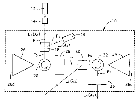
Fig. 1 through Fig. 15 show embodiments related to an optical
34
CA 02503501 2005-04-22
signal amplifying triode, and Fig. 1 shows an optical signal
amplifying triode 10 of one of the embodiments.
[0096]
In Fig. 1, a first laser light source 12 outputs a first laser
light (first input light) L1 of a first wavelength 1~1 of, for example,
1555nm, and this light is propagated via an optical fiber F1 that
is provided with a first optical modulator 14 . A second laser light
source 16 continuously outputs a second laser light (second input
light) LZ of a second wavelength 1~z of, for example, 1548nm at a
fixed intensity, and this light is propagated via a second optical
fiber F2. A wavelength variable semiconductor laser is used for
example as the first laser light source 12, and a semiconductor
laser of a single wavelength is used for example as the second laser
light source 16. The first optical modulator 14 performs, in
accordance with an electrical signal or an optical signal from an
unillustrated signal generator, intensity modulation of the first
laser light L1, which is the transmitted light, so that the light
becomes a pulse signal of the frequency of the electrical signal
or the optical signal, such as shown by the waveform of the top
stage of Fig. 3. A first optical coupler 18 functions as a first
optical input means that connects the optical fiber F1 and the optical
fiber FZ with an optical fiber F3, overlaps (multiplexes) the first
laser light L1 and the second laser light Lz, which have been propagated
through the optical fiber F1 and the optical fiber F2, and inputs
the multiplexed light into a first optical amplifier 26 via the
third optical fiber F3 and a first optical circulator 20.
[0097]
The first optical amplifier 26 is arranged from a semiconductor
optical amplifier (SOA), such as that shown in Fig. 2.
CA 02503501 2005-04-22
[0098 ]
In Fig. 2, an optical waveguide 26b, which is formed on a
semiconductorsubstrate26a arrangedfromacompoundsemiconductor,
such as indium phosphide (InP) or gallium arsenide (GaAs), is a
multi-layer film of a group III-V mixed crystal semiconductor, such
as InGaAsP, GaInNAs, AlGaInP, etc., that is epitaxially grown on
the semiconductor substrate 26a and formed to a predetermined
waveguide pattern by photolithography and is formed, for example,
to be a tape-like protrusion of predetermined width using
photolithography. Since this optical waveguide 26b is formed of
a material that is higher in refractive index than the semiconductor
substrate 26a, it has a function of propagating light while confining
the light in the thickness direction. An active layer 26c, arranged
from a pn junction, a cap layer, etc. , are included in the multilayer
film inside the optical waveguide 26b, and an upper electrode 26e
is affixed to the top. In the active layer 26c, an electron-hole
pair is formed by a voltage being applied across a lower surface
electrode 26f, affixed to the lower surface of the semiconductor
substrate 26a, and the upper electrode 26e and an excitation current
being made to flow through the pn junction, and light that passes
through the active layer 26c is amplified by an induced radiation
effect . The active layer 26c is arranged from multiple quantumwells,
strained-layer superlattice, or quantum dots. In the case of
multiple quantum wells, six pairs of InGaAs (thickness: 100A) and
InGaAsP (thickness: 100A) layers, which have been latticed-matched
by being epitaxially grown from an InP semiconductor substrate 26a,
are arranged and a guide layer (2000A) with a GRIN structure, which
is varied in composition (refractive index) in a stepwise manner,
is formed successively above the active layer 26c. The device length
36
CA 02503501 2005-04-22
(optical path length) of this active layer 26c is 600um, and it
is considered that when electrons, which are injected by energy
injection by a current value of, for example, 250mA, are moved into
a valence electron band by induced radiation by transmitted photons,
the electrons release optical energy and amplify the transmitted
light. For example, by this energy injection by a current value
of 250mA, a gain of approximately 20dB is obtained for a wavelength
of 1555nm.
[0099]
A reflecting means 26d, which is a metal film or a dielectric
multilayer film, etc., that has been processed to reflect light
by the sputtering of a metal or a dielectric, is equipped on one
end face of the first optical amplifier 26, and optical input or
optical output is thus performed via the other end face at the side
opposite the one end face. The multiplexed light of the first laser
light L1 and the second laser light LZ is thus input into the first
optical amplifier 26 via the other end face, and the light reflected
by the reflecting means 26d is again output via the other end face.
Inside the active layer 26c of this first optical amplifier 26,
spontaneous light of peripheral wavelengths centered about the
wavelength 1~1 of the first laser light L1 is generated by the incidence
of the first laser light L1, and this spontaneous light increases
or decrease in intensity in inverse proportion to the intensity
modulation of the first laser light L1. When in this state, the
second laser light L2 of the second wavelength 1~2, which is within
the wavelength range of the spontaneous light, is transmitted, this
second wavelength 1~z is reinforced while being made to vary in the
same manner as the spontaneous light . That is, light of the second
wavelength 1~2 is amplified upon being modulated in the same manner
37
CA 02503501 2005-04-22
as but inversely in phase with respect to the modulation of the
first laser light L1. The first optical amplifier 26, as well as
the second optical amplifier 34, is thus equipped with cross gain
modulation characteristics, that is, mutual gain modulation
characteristics.
[0100]
The first optical circulator 20 guides the light output from
the first optical amplifier 26 not to the third optical fiber F3
but to a fourth optical fiber F4, which is equipped with a first
wavelength selector 28. The first wavelength selector 28 is
connected to the above-described first optical amplifier 26 and
extracts light of the second wavelength A2 of 1548nm from among the
light output from the first optical amplifier 26. This first
wavelength selector 28 functions as an optical filter element and,
for example, is a fiber grating filter, which is formed by making
a portion of the fourth optical fiber F~ vary periodically in
refractive index in the longitudinal direction by localized
illumination of ultraviolet rays and selectively transmits light
at a half-width of lnm with respect to a central wavelength of the
second wavelength l~z. The first wavelength selector 28 may instead
be arranged from either a multilayer film filter, formed by layering
a plurality of layers that differ in refractive index, or a photonic
crystal, having a photonic bandgap.
[0101]
A second optical coupler 30 functions as a second optical input
means that multiplexes light of the second wavelength 1~2, which has
been selected by the first wavelength selector 28 from among the
light output from first optical amplifier 26, and the third laser
light L3, which is a control light of a third wavelength 1~3 having,
38
CA 02503501 2005-04-22
for example, a waveform among those shown in the middle stage of
Fig. 3, and inputs the multiplexed light via a fifth optical fiber
FS and a second optical circulator 32 into the second optical amplifier
34, which is arranged in the same manner as the first optical amplifier
26. At the second optical amplifier 34, the modulated second
wavelength Az is subject to further modulation by the control light
of the third wavelength A3 that is within the wavelength range of
spontaneous light centered about the second wavelength 1~2, and the
wave form of the third wavelength 1~3 becomes a waveform among those
shown in the bottom stage of Fig. 3. The second optical circulator
32 guides the light output from the second optical amplifier 34
not to the fifth optical fiber F5, but to a sixth optical fiber F6,
which is equipped with a second optical filter element 36. The second
optical filter 36 selects light of the third wavelength 1~3 from among
the light output from the second amplifier 34 and outputs this light
as output light L9 shown in the bottom stage of Fig. 3. In Fig.
3, the solid line, alternate long and short dash line, and broken
line waveforms of the control light L3 indicated in the middle stage
correspond to the solid line, alternate long and short dash line,
and broken line waveforms of the output light L9 indicated in the
bottom stage, and the output light L9 has a gain of approximately
30 times with respect to the control light L3.
[0102]
Fig. 4 and Fig. 5 illustrate the characteristics of the cross
gain modulation type wavelength conversion actions of the optical
signal amplifying triode 10 arranged in the above-described manner.
Fig. 4 is an input/output characteristics diagram of the fourth
laser light Lq with the signal strength P~ of the control light L3
as a parameter in a two-dimensional coordinate system wherein the
39
CA 02503501 2005-04-22
abscissa indicates the signal strength PIN of the first laser light
L1, which is the first input light, and the ordinate indicates the
signal strength POUT of the fourth laser light L9, which is the output
light. As is clear from the Figure, in the same manner as in a triode
amplifier, such as a transistor, the signal strength POUT of the
fourth laser light L9 responds to the variation of the signal strength
P~ of the control light L3 with the variation being amplified in
the modulation process and responds to the variation of signal
strength PIN of the first laser light L1, which is the first input
light, with the variation being amplified in the modulation process.
Also, Fig. 5 shows the frequency characteristics of the fourth laser
light L4 in a two-dimensional coordinate system wherein the abscissa
indicates the frequency of the first laser light L1, which is the
first input light, and the ordinate indicates the signal modulation
degree H ( ~ ) of the fourth laser light L9, which is the output light .
As shown in Fig. 5, lowering of the signal modulation degree H is
not seen up to 5GHz . This signal modulation degree H is expressed,
for example, by the Equation (1) shown below. In this Equation,
Imax is the maximum value of the optical signal and Imin is the minimum
value of the optical signal. In the case where quantum dots are
used in the active layer 26c, lowering of the signal modulation
degree H is not seen in the range of 100GHz and higher.
[0103]
H = 100 x ( Imax - Imin) ~ ( Imax + Imin) ~ . ~ 1
[0104]
Experiments by the present inventor have shown that when the
control light L3 is changed from the third wavelength ?~3 to the first
wavelength 1~1, the output light L4 of the first wavelength A1 is
obtained and the same optical signal amplification effect results
CA 02503501 2005-04-22
as those described above are obtained. Also, though in the above,
the second wavelength ?~2 of the second laser light LZ is shorter
than that of the first laser light L1, when the second wavelength
1~2 of the second laser light LZ is made longer than that of the first
laser light L1, not only are the same optical signal amplification
effect results as those described above obtained but a further effect
that the minimum value, for example, of the waveform of the bottom
stage of Fig. 3 approaches zero, in other words, the effect that
the baseline of the output light L9 approaches zero, like that of
the first laser light L1, is also obtained. Also, when signal
modulation is applied to the third input light L3 of the third
wavelength 1~3 with the first input light L1 of the first wavelength
1~1 being a continuous light (bias light) like the second laser light
Lz of the second wavelength A2, the signal of the third input light
L3, amplified by a gain of 10 or more, is output as the output light
L9 of the third wavelength A3.
[0105]
Fig. 6 (a} shows a flip-flop circuit 42 arranged from two optical
NAND gates 40 to which the above-described optical signal amplifying
triode 10 is applied, and Fig. 6(b) shows a flip-flop circuit 46
arranged from two optical NOR gates 44. As is well known, a NAND
gate and a NOR gate in an electronic circuit are respectively arranged
from a plurality of transistors, and the optical HAND gates 40 and
the NOR gates 44 are arranged by providing the above-described optical
signal amplifying triodes 10 in place of transistors in optical
circuits, and the flip-flop circuits 42 and 46 are arranged from
a pair of optical NAND gates 40 and a pair of optical NOR gates
44, respectively. With these flip-flop circuits 42 and 46,
information are recorded by means of light.
41
CA 02503501 2005-04-22
[0106]
Fig. 7 shows an optical operational amp 48 to which the
above-described optical signal amplifying triode 10 is applied.
As is well known, an operational amp in an electronic circuit is
arranged from a plurality of transistors, and the optical operational
amp 48 is arranged by providing the above-described optical signal
amplifying triodes 10 in place of transistors in an optical circuit.
[0107)
With the optical signal amplifying triode 10 of Fig. l, arranged
as described above, when light of the second wavelength 1~2, selected
from among the light from the first optical amplifier 26 into which
the first input light L1 of the first wavelength 1~1 and the second
input light LZ of the second wavelength 1,2 are input, and the third
input light (control light) L3 of the third wavelength h3 are input
into the second optical amplifier 34, the output light L9 of the
third wavelength A3 that is selected from among the light output
from the second optical amplifier 34 is light that is modulated
in response to the intensity variation of either or both of the
first input light L1 of the first wavelength 1~1 and the second input
light LZ of the second wavelength 1~2 and is a signal with which the
signal gain with respect to the third input light (control light)
L3 of the third wavelength A3 is 2 or more. The optical signal
amplifying triode 10, which can perform an amplification process
on an optical signal directly using control input light, can thus
be provided.
[0108]
Also with the optical signal amplifying triode 10 of the present
embodiment, since the first input light L1 of the first wavelength
hl is modulated light, the second input light Lz of the second
42
CA 02503501 2005-04-22
wavelength 1~z is continuous light, the third input light L3 of the
third wavelength 1~3 is control light, and the output light Lq of
the third wavelength 1~3 has, in the input interval of the control
light L3, a signal waveform with which the modulated signal of the
first input light L1 is amplified, the output light Lq of the third
wavelength A3 is amplified light that is modulated in response to
the intensity variation of the first input light L1 of the first
wavelength A1 in the input interval of the control light L3. The
optical signal amplifying triode 10, which can perform a switching
process on an amplified optical signal directly using control input
light, can thus be provided.
[0109]
Also with the present embodiment, since the first wavelength
?~1 and the third wavelength ?~3 can be made the same, the first input
light L1, which is the signal input light into the optical signal
amplifying triode 10, the third input light L3, and the output light
L9 can be made the same in wavelength, thus enabling a plurality
of the optical signal amplifying triodes 10 to be connected with
a common wavelength and an optical circuit of a high degree of
integration to be arranged from a plurality of optical signal
amplifying triodes 10.
[0110]
Also with the present embodiment, the second wavelength AZ
can be made longer than the first wavelength ?~1, and in this case,
the merit that the waveform indicated by the output light L3, which
is the amplified light of the modulated first input light L1, has
a baseline close to the zero level like the baseline of the waveform
of the first input light is provided. The merit of making the
modulation degree large is thus provided.
43
CA 02503501 2005-04-22
[0111]
Also with the present embodiment, since the signal gain of
the output light LQ of the third wavelength ?~3 with respect to the
control light L3 of the third wavelength ?~3 takes on a value of 10
or more, the amplification function of the optical signal amplifying
triode is increased further and the scope of application thereof
is expanded.
[0112]
Also with the present embodiment, since each of the first
optical amplifier 26 and the second optical amplifier 34 is a
semiconductor opticalamplifierequipped withan activelayerformed
of a pn junction, the optical signal amplifying triode 10, with
which the signal gain and the response speed are increased further,
can be obtained.
[0113]
Also with the present embodiment, since the active layer 26c
of each of the first optical amplifier 26 and the second optical
amplifier 34 is arranged from quantum wells or quantum dots, the
optical signal amplifying triode 10, with which the signal gain
and the response speed are increased further, can be obtained. In
particular, a response speed of 100GHz or more can be obtained when
quantum dotsare used. Also,thepolarization dependenceislessened
when a strained-layer superlattice is used as the active layer.
[0114]
Also with the present embodiment, since each of the first
optical amplifier 26 and the second optical amplifier 34 has equipped,
on one end face thereof, a mirror or other reflecting means 26d,
formed by metal deposition, etc., in order to reflect light
transmitted via the active layer 26c, and the input light is input
44
CA 02503501 2005-04-22
and the output light is taken out from the other end face, the
transmission path in the active layer 26c is elongated practically
by the mirror or other reflecting means 26d equipped on the one
end face and the signal gain is increased further. Also, the
modulation degree is increased further by the feedback effect.
[0115]
Also with the present embodiment, since the optical circulators
20 and 32, into which the input light is input upon transmission
via the other end faces of the first optical amplifier 26 and the
second optical amplifier 34 and which guide the light output through
the other end faces to optical paths that differ from those of the
input light, are provided, the light output from the other end faces
of the first optical amplifier 26 and the second optical amplifier
34 are prevented from entering the waveguides that guide light to
be input into the other end faces and are mainly guided to other
waveguides for output.
[0116]
Also with the present embodiment, since either or each of the
first wavelength selection element 28 and the second wavelength
selection element 36 is arranged from a grating filter, with which
the refractive index of the interior of a waveguide or optical fiber
is made to vary periodically in the light propagation direction,
a multilayer filter, formed by layering a plurality of layers that
differ in refractive index, or a photonic crystal, having a photonic
bandgap, the second wavelength 1~2 or the third wavelength 1~3 is
extracted favorably from the light from the first optical amplifier
26 or the second optical amplifier 34.
[0117]
Also, the above-described optical signal amplifying triodes
CA 02503501 2005-04-22
can be used to arrange the optical NAND gate 40, the flip-flop
circuit 42, formed of a pair of optical NAND gates 40, or the optical
operational amp 46 and can thereby heighten the functions of an
optical integrated circuit.
[0118]
Also with the first optical amplifier 26 of the present
embodiment, since the second wavelength 1~2 is a wavelength within
the wavelength range of the peripheral light of the first input
light L1 of the first wavelength 1~1 and with the second optical
amplifier 34, the third wavelength 1~3 is a wavelength within the
wavelength range of the input light of the second wavelength A2,
a signal of the second wavelength 1~z or the third wavelength ?~3 that
is contained in the output light from the first optical amplifier
26 or the second amplifier 34 is amplified favorably.
[0119]
In the case where the reflecting means 26, disposed at the
one end face of the first optical amplifier 26 is arranged from
a wavelength selective reflecting film that transmits light of the
first wavelength A1 but reflects light of the second wavelength l~z,
the first wavelength selector 28 is made unnecessary. When the
reflecting means of the second optical amplifier 34, arranged in
the same manner as the first optical amplifier 26, is arranged from
a wavelengthselectivereflectingfilm(wavelengthselective mirror)
that transmits light of the second wavelength 1~2 but reflects light
of the third wavelength 1~3, the second wavelength selector 36 is
made unnecessary. The above-mentioned wavelength selective
reflecting film is formed, for example, of a dielectric multilayer
film in which dielectric layers that differ in refractive index
are layered in an alternating manner.
46
CA 02503501 2005-04-22
[0120]
Another embodiment shall now be described. In the following
description, portions in common to the above-described embodiment
shall be provided with the same symbols and description thereof
shall be omitted.
[0121]
Fig. 8 shows the principal parts of an arrangement example
of an optical signal amplifying triode 50 of another embodiment
of the above-described optical signal amplifying triode 10. With
the optical signal amplifying triode 50 of the present embodiment,
an optical signal LA is input via a half mirror 51 and a converging
lens 52, which serve as the first optical input means, into one
end face of the first optical amplifier 26. Among the light output
from the other end face of the first optical amplifier 26 and via
a converging lens 53, light of the first wavelength ?~1 is transmitted
and light of a wavelength Ab of a bias light L2 is reflected by a
wavelength selective mirror 54, which functions as the first
wavelength selector, and returned to the first optical amplifier
26. The light that is output from the one end face of the first
optical amplifier 26 is reflected by the half mirror 51, multiplexed
by a control light L~ by a half mirror 55, which functions as the
second optical input means, and made incident on one end face of
the second optical amplifier 34 via a converging lens 56. Among
the light output from the other end face of the second optical
amplifier 34 and via a converging lens 57, light of the wavelength
Ab of the bias light LZ is transmitted, and the component of the
same wavelength as the control light L~ is reflected by a wavelength
selective mirror 58, which functions as the second wavelength
selector, and returned to the second optical amplifier 34 . The output
47
CA 02503501 2005-04-22
light L3, output from the one end face of the second amplifier 34
will be the same as that of the above-described optical signal
amplifying triode 10. The wavelength converter 50, arranged as
described above, provides the same cross gain modulation type
wavelength conversion action and optical amplification action as
those of the above-described optical signal amplifying triode 10.
The wavelength selective mirror 58 and the wavelength selective
mirror 54 are optically coupled to the end face of the second optical
amplifier 34 and the end face of the first optical amplifier 26
via the converging lens 57 and the converging lens 53 . The converging
lenses 52, 53, 56, and 57 are arranged, for example, frommicrolenses
and the optical signal LA, the output signal L3, etc. , are transmitted
by optical fibers. The half mirrors 51 and 55 may be replaced by
optical couplers or optical circulators.
[0122]
Fig. 9 shows the principal parts of an arrangement example
of an optical signal amplifying triode 59 of another embodiment
of the above-described optical signal amplifying triode 10. The
optical signal amplifying triode 59 of the present embodiment
comprises the first optical amplifier 26 and the second optical
amplifier 34, which are positioned in series, optical couplers 60
and 61, which make the optical signal LA and the bias light Lb
(wavelength: 1~b) be incident on the inner end face of the first optical
amplifier 26, a wavelength selective reflector 62, which, from among
the light from the outer end face of the first optical amplifier
26, transmits light of the first wavelength 1~1 but reflects the
component of the wavelength Ab and returns it into the first optical
amplifier 26, a filter 63, which transmits the component of wavelength
1~b among the light emitted from the inner end face of the first optical
98
CA 02503501 2005-04-22
amplifier 26 and makes it incident on the inner end face of the
second optical amplifier 34, an optical coupler 64, which makes
the control light L~ incident on the outer end face of the second
optical amplifier 34, and a filter 65, which transmits light of
the same wavelength component as the control light L~ among the light
emitted from the outer end face of the second optical amplifier
34 and outputs it as the output light L3. The optical couplers 60
and 61 function as the first optical input means, the optical coupler
64 functions as the second optical input means, and the reflector
62 and the filter 65 function as the first wavelength selector and
the second wavelength selector. The wavelength converter 59,
arranged as described above, provides the same cross gain modulation
type wavelength conversion action and optical amplification action
as those of the above-described optical signal amplifying triode
10. The optical signal of the wavelength 1~~ of the control light
L~ is reflected by the filter 63 and output upon transmission through
the filter 65. The optical component of the wavelength Ab is not
transmitted through the filter 65. The optical couplers 60 and 61
may be arranged from a single optical coupler.
[0123]
Fig. 10 shows an example where the above-described optical
signal amplifying triode 59 is arranged as a monolithic structure
of the same type as the first optical amplifier 26 of monolithic
structure that is shown in Fig. 2, that is, as a single chip structure
onthe semiconductor substrate 26a. With this embodiment's optical
signal amplifying triode 59 of monolithic structure, the reflector
62, the filter 63, and the filter 65, each arranged from a grating
that is varied periodically in refractive index, are disposed
successively at a position at the outer side of the first optical
49
CA 02503501 2005-04-22
amplifier 26, a position between the first optical amplifier 26
and the second optical amplifier 34, and at a position at the outer
side of the second optical amplifier 34. The pair of branch
waveguides that are branched from the straight optical waveguide
26b correspond to the optical couplers 60 and 61 and the optical
coupler 64.
[0124]
Fig. 11 shows the principal parts of an arrangement example
of an optical signal amplifying triode 66 of another embodiment
of the above-described optical signal amplifying triode 10. The
wavelength converter 66 of the present embodiment comprises a pair
of reflecting type first optical amplifier 26 and second optical
amplifier 34, a four-terminal optical circulator 67, which is
equipped with four terminals, including a second terminal 67b and
a third terminal 67c that are connected to the pair of reflecting
type first optical amplifier 26 and second optical amplifier 34
and which although transmitting light across the four terminals,
makes the exit light from a certain terminal differ in optical path
from the light incident onto that terminal, an optical coupler 68,
which multiplexes the optical signal LA and the bias light Lb
(wavelength 1~b) and makes the multiplexed light incident onto the
first terminal (first port) 67a of the four-terminal optical
circulator 64, and an optical coupler 69, which multiplexes light
of the wavelength Ab that propagates from the reflecting type first
optical amplifier 36 to the second port 67b of the four-terminal
optical circulator 67 with the control light L~ and makes the
multiplexed light incident onto the second optical amplifier 34,
and makes light of the same wavelength component as the control
light LC be transmitted from the fourth port 67d of the four-terminal
CA 02503501 2005-04-22
optical circulator 67 . A reflecting film 26d, which transmits light
of the first wavelength 1~1 but selectively reflects light of the
second wavelength lib, is disposed on the reflecting surface of the
first optical amplifier 26, and a reflecting film 34d, which transmits
light of the second wavelength 1~b but selectively reflects light
of the same wavelength 1~~ component as the control light L~, is disposed
on the reflecting surface of the second optical amplifier 34. The
optical signal amplifying triode 66, arranged as described above,
provides the same cross gain modulation type wavelength conversion
action and optical amplification action as those of the
above-described optical signal amplifying triode 10, and the
modulation degree of the output light L3 is increased due to passage
through thefour-terminalopticalcirculator67. Thisembodiment's
optical signal amplifying triode 66 provides the merit of being
simple in arrangement in comparison to the optical signal amplifying
triode 10 of Fig. 1. The optical coupler 69 may be arranged to
multiplex the control light L~ with light of wavelength 1~b that
propagates from the third port 67c of the four-terminal optical
circulator 67 to the second optical amplifying element 34. With
the present embodiment, the optical coupler 68 and the optical coupler
69 function as the first optical input means and the second optical
input means, and the reflecting films 26d and 34d function as the
first wavelength selector and as the second wavelength selector.
[0125]
Fig. 12 shows an example where the above-described optical
signal amplifying triode 66 is arranged as a monolithic structure.
As with the above-described arrangements of Fig. 6 and Fig. 10,
this optical signal amplifying triode 66 of monolithic structure
is equipped with the optical waveguide 26b formed on the semiconductor
51
CA 02503501 2005-04-22
substrate 26a. This optical waveguide 26b is provided with a Z-like
portion for providing the same function as the four-terminal optical
circulator 67 and branch waveguides, which are branched from portions
of the Z-like portion, for providing the functions of the optical
couplers 68 and 69. At the refraction point of the Z-like portion
of the optical waveguide 26b, the pair of reflecting type first
optical amplifier 26 and second optical amplifier 34 are arranged
in the same manner as those shown in Fig. 2 and Fig. 10 described
above. The reflecting films 26d and 34d are provided at the outer
end faces of the reflecting type first optical amplifier 26 and
second optical amplifier 34.
[0126]
Fig. 13 shows the principal parts of an arrangement example
of an optical signal amplifying triode 70 of another embodiment
of the above-described optical signal amplifying triode 10. The
optical signal amplifying triode 70 of the present embodiment
comprises the first optical amplifier 26 and the second optical
amplifier 34, respectively formed by providing a first optical
waveguide 72 and a second optical waveguide 73 by shaping mixed
crystal semiconductor layers, each having a pn junction layer (active
layer) of, for example, GaInNAs grown on a rectangular semiconductor
substrate 71 of, for example, GaAs, to a V-like shape by
photolithography, and providing first optical waveguide 72 and
second optical waveguide 73 with unillustrated electrodes, a
wavelengthselective reflectingfilm74, disposedatanintersecting
portion of the first optical waveguide 72 and the second optical
waveguide 73 at one end face of the rectangular semiconductor
substrate 71 and reflecting the control light L~ and light of the
second wavelength 1~b of the bias light Lb towards second optical
52
CA 02503501 2005-04-22
waveguide 73 but selectively transmitting light of the first
wavelength A1 of the optical signal LA, and a wavelength selective
reflecting film 75, disposed at the output side of the second optical
waveguide 73 at one end face of the rectangular semiconductor
substrate 71 and reflecting light of the second wavelength Ab but
transmitting light of the same wavelength component as the control
light L~. The optical signal LA and bias light Lb are multiplexed
by an optical coupler 76 and then made incident onto an end face
of optical waveguide 72, and the control light L~ is made incident
into the second waveguide 73 from an optical coupler 77, disposed
at the outer side of the wavelength selective reflecting film 75.
The optical signal amplifying triode 70, arranged as described above,
provides the same cross gain modulation type wavelength conversion
action and optical amplification action as those of the
above-described optical signal amplifying triode 10. Also, since
this embodiment' s optical signal amplifying triode 70 is arranged
as a single chip by processing mixed crystal semiconductor layers,
each having a pn junction layer (active layer) formed of a group
III-V mixed crystal layer, such as GaInNAs, grown on the rectangular
semiconductor substrate of, for example, GaAs, by photolithography
and providing electrodes, the merit of enabling an arrangement of
extremely small size is provided. With the present embodiment, the
optical couplers 76 and 77 function as the first and second optical
input means and the wavelength selective reflecting film 74 and
the wavelength selective reflecting film 75 function as the first
wavelength selector and the second wavelength selector.
[0127]
Fig. 14 shows the principal parts of an arrangement example
of an optical signal amplifying triode 78 of another embodiment
53
CA 02503501 2005-04-22
of the above-described optical signal amplifying triode 10. With
the optical signal amplifying triode 78 of the present embodiment,
the optical signal LA is input into one end face of the first optical
amplifier 26 via an optical coupler 79, used as a multiplexer, an
optical coupler 80, used as an optical splitter, and the converging
lens 52, and among the light output from the other end face of the
first optical amplifier 26 and via the converging lens 53, the
wavelength 1~1 of the above-mentioned optical signal LA is not
transmitted (is absorbed) by a wavelength selective filter 81 and
light of the wavelength 1~b of the bias light is transmitted through
the filter 81, reflected by a total reflecting mirror 82, and returned
to the first optical amplifier 28. Light that is output from the
one end face of the first optical amplifier 26 is transmitted from
the optical coupler 80 to another optical coupler 83 and multiplexed
there with the control light L~. The light is then made incident
on one end face of the second optical amplifier 34 through an optical
coupler 84 and the converging lens 56. Among the light output from
the other end face of the second optical amplifier 34 and through
converging lens 57, light of the wavelength 1~b of the bias light
is not transmitted ( is absorbed) by a wavelength selective filter
85 and component of the same wavelength A~ as control light L~ is
transmitted through the filter 85, reflected by a total reflecting
mirror 86, and returned to the second optical amplifier 34. The
output light L3, which is output from the one end face of the second
optical amplifier 34 is output via an optical coupler 84 to an external
optical distributor 150, such as that described below. The optical
signal amplifying triode 78, arranged as described above, not only
provides the same cross gain modulation type wavelength conversion
action and optical amplification action as those of the
54
CA 02503501 2005-04-22
above-described optical signal amplifying triode 10 but also
provides that merit that the characteristics are improved further
due to the wavelength 1~1 of the optical signal LA being absorbed
and not transmitted by wavelength selective filter 81 and the
proportion thereof that returns to the first optical amplifier 26
side thus being made extremely small . With the present embodiment,
the optical coupler 79 and the optical coupler 84 function as the
first optical input means and the second optical input means and
the wavelength selective filter 81 and the wavelength selective
filter 85 function as the first wavelength selector and the second
wavelength selector.
[0128]
Fig. 15 shows the principal parts of an arrangement example
of another embodiment of the above-described optical signal
amplifying triode 10, which is a monolithic structure wherein a
plurality (two in the present embodiment) of optical signal
amplifying triodes 88 are integrated in a single chip. Each of the
plurality of optical signal amplifying triodes 88 of the present
embodiment comprises the first optical amplifier 26, the second
optical amplifier 34, and a third optical amplifier 93, respectively
formed by providing a first optical waveguide 90, a second optical
waveguide 91, and a third optical waveguide 92 by shaping, by
photolithography, mixed crystal semiconductor layers, each having
a pn junction layer (active layer) of, for example, GaInNAs grown
on a rectangular semiconductor substrate 89 of, for example, GaAs,
into straight lines, extending from one end face to the other end
face and forming V-like shapes in adjacent pairs, and by providing
the first optical waveguide 90, the second optical waveguide 91,
and the third optical waveguide 92 with unillustrated electrodes,
CA 02503501 2005-04-22
a wavelengthselective reflectingfilm(wavelengthselective mirror)
94, disposed at an intersecting portion of the first optical waveguide
90 and the second optical waveguide 91 and across the output side
end face of the third optical waveguide 92 at one end face of the
rectangular semiconductor substrate 89 and reflecting the control
light L~ and light of the second wavelength 1~b of the bias light
Lb towards the second optical waveguide 91 and selectively
transmitting the control light L~ and light of the first wavelength
hl of the optical signal LA, and a wavelength selective reflecting
film (wavelength selective mirror) 95, disposed at the output side
end face of the second optical waveguide 91 at one end face of the
rectangular semiconductor substrate 89 and transmitting light of
the second wavelength 1~b but reflecting light of the same wavelength
component as the control light L~ to the third optical waveguide
92. The optical signal LA and bias light Lb are multiplexed by an
optical coupler 96 and then made incident onto the input side end
face of the first optical waveguide 90 and the control light L~ is
made incident into the second optical waveguide 91 from the exterior
of the wavelength selective reflecting film 94. Each of the optical
signal amplifying triodes 88, arranged as described above, provides
the same cross gain modulation type wavelength conversion action
and optical amplification action as those of the above-described
optical signal amplifying triode 10 . Also, since this embodiment' s
optical signal amplifying triodes 88 are arranged as a single chip
by processing mixed crystal semiconductor layers, each having a
pn junction layer (active layer) formed of a group III-V mixed crystal
layer, such as GaInNAs, grown on a rectangular semiconductor
substrate of, for example, GaAs, by photolithography and providing
electrodes, the merit of enabling the optical signal amplifying
56
CA 02503501 2005-04-22
triode 10, which can perform signal processing of optical signals
of, for example, the l.3um band, to be arranged at an extremely
small size is provided. Also with this embodiment, a circulator
is made unnecessary and a higher output is enabled by the three
optical amplifiers 26, 34, and 93. With the present embodiment,
the optical coupler 96 functions as the first optical input means,
the wavelength selective reflecting film 94 functions as the second
optical input means and the first wavelength selector, and the
wavelength selective reflecting film 95 functions as the second
wavelength selector.
[0129]
Fig. 16 to Fig. 33 illustrate embodiments related to an optical
signal transfer method and an optical signal router, that is, an
optical signal relay (transfer) device for favorably carrying out
the optical signal transfer method, and with these embodiments,
optical communication for advanced information processing is enabled
by the transferring of a optical signal train, which has been
transmitted via a predetermined transmission path, to transmission
paths, among a plurality of transmission paths, that correspond
to the routing information contained in the optical signal.
[0130]
Fig. 16 is a diagram that schematically shows an optical signal
relay (transfer) device 110 that is disposed between input optical
fibers FAl to F~, which are a plurality of transmission paths in
one optical network, and output optical fibers FB1 to FBM, which are
a plurality of transmission paths in another optical network, and
transfers each of wavelength multiplexed optical signals (laser
light) LA1 to L~, transmitted via any of the input optical fibers
FA1 to F~, to a wavelength bus in an output optical fiber among the
57
CA 02503501 2005-04-22
output optical fibers FB1 to FBM that has been determined based on
routing information added by amplitude modulation to the optical
signal. This optical signal relay device 110 is also referred to
as an optical signal router.
[0131]
In Fig. 16, each of the optical signals LA1 to L~,,, transmitted
via any of input optical fibers FAl to F~, is a wavelength division
multiplexed (WDM) signal in which optical signals of a predetermined
plurality of types of wavelengths are overlapped. Thus for example,
an optical signal LAii of the wavelength 1~1 among a series of
predetermined wavelengths contained in the optical signal LA1 is,
in accordance with routing information provided by amplitude
modulation being applied to a label portion or tag portion thereof,
transferred to a wavelength bus in an optical fiber FB among the
output optical fibers FB1 to FBM, that is, transferred at a wavelength
among a predetermined plurality of types, that is, N types of
wavelengths 1~1 to 1~N. Wavelength multiplexed optical signals ( laser
light) LB1 to LBM are transmitted by means of the output optical fibers
FB1 to FBM, respectively.
[0132]
In addition to M optical splatters (AWGs: Arrayed Waveguide
Gratings) S1 to SM, which separate the wavelength multiplexed optical
signals LAl to L~, transmitted from the predetermined number, that
is, the M input optical fibers FA1 to F~, respectively into optical
signal trains (packets) according to the N types of wavelengths
2~1 to 1~N, so that, for example, the optical signal LA1 is separated
into LAii to LplNi the optical signal relay device 110 comprises M
relays of first relay R1 to Mth relay RM, which perform wavelength
conversion of the optical signal trains (packets) LAlI to LAIN of
58
CA 02503501 2005-04-22
N types of wavelengths 1~1 to AN in accordance with the routing
information attached to the optical signal trains by amplitude
modulation and perform addition of the prior routing information
or new routing information by amplitude modulation, and M
multiplexers (AWGs) T1 to TM, which multiplex the optical signals
output from first relay R1 to Mth relay RM and guide the multiplexed
signals to output optical fibers FB1 to FBM.
[0133]
Fig. 17 is a diagram illustrating the arrangement of a first
relay Rl, disposed at a position between the input optical fiber
FA1 and the output optical fiber FB1, as a representative example
for describing the arrangement of the first relay R1 to Mth relay
RM, which are arranged in the same manner as each other. In Fig.
17, the first relay R1, is equipped with N main relay units, that
is, first main relay unit RB11 to Nth main relay unit RB1N, which
are arranged in the same manner as each other, and when the optical
splitter S1 separates the wavelength multiplexed optical signal LA1,
transmitted from the input optical fiber FA1, into the optical signal
trains (packets) LAii to LA1N in accordance with the N types of
wavelengths ?~1 to 1~N, and these signal trains are input via optical
fibers FAii to FA1N~ the main relay units perform wavelength conversion
of the optical signals LAii to LAIN in accordance with the routing
information attached to the label portions or tag portions of the
optical signals by amplitude modulation and output optical signals
upon adding, by amplitude modulation, the same routing information
as those up until now or new routing information. The output signals
of any of the wavelengths of the N types of wavelengths hl to 1~N,
which have been output respectively from the first main relay unit
RB11 to the Nth main relay unit RB1N, are connected to the multiplexer
59
CA 02503501 2005-04-22
T1 respectively via N X N cross-connected fibers Flit to FNN1 for
transmitting optical signals that have been branched according to
the wavelength and the routing information. The output signals from
the first main relay unit RB11 to the Nth main relay unit RB1N are
thus transmitted at the desired wavelengths via the desired output
optical fibers among the output optical fibers Fell to FBN1 to the
multiplexes T1. The main relay units RBzl to RBMN that make up the
other relays Rz to RM are likewise connected to the multiplexers
Tz to TM respectively via N X N cross-connected fibers Fliz to FNMZ . . .
N x N cross-connected fibers Flits to FNNM- As shown in Fig. 17, the
output ends of, for example, the cross-connected fibers F111, Fzii, . . .
FNii. which transmit signals of the same wavelength, that is, the
wavelength 1~1, are coupled together and input via the fiber Fell into
the multiplexes T1. The output ends of the cross-connected fibers
FiNi. Fzrn. . . . FNrri. which transmit signals of wavelength 1~N, are coupled
together and input via the fiber FBN1 into the multiplexes T1.
[0134]
The optical splitter S1 is a well-known optical splitting
circuit that is arranged, for example, using an angular dispersion
element, such as a diffraction grating, prism, etc., a wavelength
selective reflecting/transmitting film, such as an interference
filter arranged froma dielectricmultilayer film, etc. , or an optical
waveguide type optical splitting circuit, etc. The multiplexes T1
is arranged, for example, from an optical directional coupling
circuit, having microlensesasprincipal components, a distribution
coupling type optical multiplexing coupler, wherein portions of
a plurality of optical fibers disposed in parallel are coupled
together locally, or a concentrated coupling type optical
multiplexing coupler that makes use of multiple reflection at the
CA 02503501 2005-04-22
inner walls of a rectangular tube or mixing in a flat plate.
[0135]
Also, the first main relay unit RB11 is arranged, for example,
as shown in Fig. 18. In Fig. 18, the optical signal LAll, input from
the optical splitter S1 via the optical fiber FAIL, is connected
successively to a first optical coupler 114, which functions as
an optical splitter/coupler, an optical delay element 116, and a
cross gain modulation type wavelength converter (optical switching
device or main optical signal amplifying triode unit) 118. The first
optical coupler 114 is arranged from a branching circuit, having
optical fibers as principal components, or a branching circuit,
having microlenses as principal components, etc. A branching
circuit having optical fibers as principal components is arranged,
for example, by putting a pair of optical fibers into a parallel
state of mutual close contact with each other or into a state of
mutual close contact by twisting the fibers mutually in spiral form
over a predetermined interval and disposing a reflecting film that
can transmit and ref lect at a branching point of the f fibers . With
a branching circuit having microlenses as principal components,
for example, light that has been formed into a parallel beam by
means of a converging rod lens is branched using a wedge type
refracting surface or reflecting surface. Since this first optical
coupler 114 is equipped with bidirectionality, that is, with
reversibility, it functions as a multiplexer, which, when optical
signals are propagated in an opposite direction, multiplexes the
optical signals and makes the multiplexed signal propagate in the
opposite direction inside a first optical fiber 112.
[0136]
The optical delay element 116 delays an optical signal,
61
CA 02503501 2005-04-22
transmitted inside the above-mentioned optical fiber FAii by just
a predetermined amount of time and is arranged, for example, by
winding an optical fiber of predetermined length and thereby
providing a propagation distance to delay the optical signal by
the propagation time it takes for the optical signal to propagate
across the predetermined propagation distance. The delay time of
the optical delay element 116 is determined by experiment in advance
so that the optical signal to be subject to wavelength conversion
inside the wavelength converter 118 will be synchronized with the
control light that indicates the transmission destination of the
optical signal.
[0137]
The branched optical signal that is branched by the first
optical coupler 114 from the optical signal inside the optical fiber
FAll is supplied to an electronic controller 124, via an optical
fiber 120 and a photoelectrical signal converter 122 connected
thereto. The electronic controller 124 is, for example, arranged
from a so-called microcomputer, wherein a CPU processes the input
signal in accordance with a program stored in advance in a ROM and
using the temporary storage function of a RAM. Based on a code signal,
that is, routing information indicated by amplitude modulation and
contained in the optical signal transmitted via the optical fiber
120, the electronic controller 124 supplies a wavelength command
signal, corresponding to the routing information for routing the
optical signal, to a control light generator 126. Since the
electronic controller 124 extracts, for example, just the amplitude
modulation signal contained in the optical signal LAii input from
the optical fiber 120 and makes the control light L~, which is in
accordance with the wavelength corresponding to the routing
62
CA 02503501 2005-04-22
information indicated by the amplitude modulation, be generated
from the control light generator 126, electromagnetic waves
corresponding to signals besides the address signal are not
generated.
[0138]
The control light generator 126 has a control light source
that outputs the control light L~ of a plurality of priorly set types
of wavelengths A~ and, in accordance with the command signal from
the electronic controller 124, that is, in accordance with the
wavelength command signal selected in accordance with the branching
information contained in the optical signal L1, supplies control
light L~ of wavelengths 1~~ corresponding to the branching information
to the wavelength converter 118. The control light generator 126
generates in an alternative or selective manner, the control light
L~ of a plurality of types, for example, N types of wavelengths 1~~1,
~~3. . . ~ ~~N in correspondence to the number of wavelength buses
inside the transfer destination output optical fibers Fs1 to FHM-
Fig. 19, Fig. 20, and Fig. 21 respectively illustrate arrangement
examples of the control light generator 126.
[0139]
In Fig. 19, the control light generator 126 comprises a
plurality of laser light sources 126L1 to 126Ln, which are the control
sources that output light, each of a single wavelength and differing
from each other in wavelength, a plurality (N units) of optical
modulators 126M1 to 126Mn, respectively being disposed at the output
sides of the respective laser light sources 126L1 to 126Ln to perform
switching of the respective output light of laser light sources,
and a single optical multiplexer 1265, which multiplexes the light
transmitted via optical modulators 126M1 to 126Mn, and, by the
63
CA 02503501 2005-04-22
operation of laser light sources 126L1 to 126Ln and optical modulators
126M1 to 126Mn in accordance with the branching command signal from
the electronic controller 124, outputs control light L~ of wavelengths
h~ that have been selected in accordance with the routing information
(branching information) indicated by the amplitude modulation
signals contained in the optical signal LAlI. Semiconductor laser
diodes are used, for example, as the plurality of laser light sources
126L1 to 126Ln. In Fig. 20, the control light generator 126 comprises
the plurality of laser light sources 126L1 to 126L", which correspond
to being the control light sources that output light, each of a
single wavelength and differing from each other in wavelength, the
single optical multiplexer 1265, which multiplexes the light output
from the laser light sources 126L1 to 126Ln in a single waveguide,
and a single optical modulator 126M, which is disposed at the output
side of the optical multiplexer 1265 and performs switching of the
output light to cut off the blanking interval, and, by the operation
of the laser light sources 126L1 to 126Ln and the optical modulator
126 in accordance with the branching command signal from the
electronic controller 124, outputs control light L~ of wavelengths
1~~ that have been selected in accordance with the branching
information contained in the optical signal LAlI. In Fig. 21, the
control light generator 126 comprises a wavelength variable laser
light source 126L~, with which the wavelength of the output light
can be varied, and the single optical modulator 126M, which is disposed
at the output side of the wavelength variable laser light source
126L~ and performs switching of the output light to cut off the blanking
interval, and, by the operation of the wavelength variable laser
light source 126z~ and the optical modulator 126M in accordance with
the branching command signal from the electronic controller 124,
64
CA 02503501 2005-04-22
outputs control light L~ of wavelengths A~ that have been selected
in accordance with the branching information contained in the optical
signal L1. For example a distributed Bragg reflection laser, a
micromachine surface emission laser, a thermally tuned DFB laser,
etc. , is used as the wavelength variable laser light source 126LV.
With a distributed Bragg reflection laser, an electric current is
injected in to a DBR layer (Bragg reflection layer) that makes up
one of a pair of mirrors that make up an optical oscillator of the
laser and the refractive index of this portion is varied by a plasma
effect to vary the optical oscillation wavelength. With a
micromachine surface emission laser, the optical oscillation
frequency is varied by the variation of the optical oscillator length
by a micromachine. With a thermally tuned DFB laser, the optical
oscillation wavelength is varied by a refractive index variation
due to temperature. Each of the optical modulators 126M1 to 126Mn
and 126M is arranged, for example, from a semiconductor optical
modulator, with which transmitted light is switched on or off by
a drive current or a drive voltage being applied to a pn junction
portion, an externally modulated optical modulator, with which
transmitted light is switched on or off by the application of a
drive voltage from the exterior to lithium niobate or other
monocrystal or substance that exhibits an electrooptical effect.
[0140]
Along with the optical distributor 150, which also functions
as the second wavelength selector, the optical wavelength converter
118 of Fig. 18 makes up an optical signal amplifying triode 128,
which is basically arranged in the same manner as any of the optical
signal amplifying triodes 10, 50, 59, 66, 70, 78, and 88 shown in
Fig. 1 and Fig. 8 to Fig. 15. As shown in Fig. 22, the present
CA 02503501 2005-04-22
embodiment' s optical wavelength converter 118 has a pair of first
optical amplifier 136 and second optical amplifier 144, which
correspond to being the plurality of optical amplifiers that make
use of cross gain modulation characteristics to amplify, perform
wavelength conversion, and output light that has been input via
first optical fiber 112, equipped in series and is arranged to amplify
the optical signal input via the first optical fiber 112 and output
the light L3 of the same wavelength as the control light L~ in
synchronization with the input of the control light L~ corresponding
to the branching information contained in the optical signal. That
is, in Fig. 22, a laser light source 130 is arranged from a
single-wavelength semiconductor laser and performs continuous
output at fixed intensity of a laser light (second input light)
LZ of a wavelength 1~2 of, for example, 1565nm that is longer than
the wavelength 1~1 of, for example, 1555nm, of the optical signal
L1 (first input light) . A third optical coupler 132 functions as
the first optical input means that overlaps (multiplexes ) the optical
signal L1, which had been amplitude modulated and transmitted inside
the first optical fiber 112, with the laser light L2, which is
continuous light, and outputs the multiplexed light to the first
optical amplifier 136 via the first optical circulator 34.
[0141]
As with the first optical amplifier 26, shown in Fig. 2, each
of the first optical amplifier 136 and the second optical amplifier
144 is arranged from a semiconductor optical amplifier (SOA) . Since
the first optical amplifier 136 is equipped on one end face thereof
with a reflecting means 136d, which is a mirror having an end face
treatment for reflection of light applied thereto by sputtering,
etc. , input of light or output of light is carried out through the
66
CA 02503501 2005-04-22
other end face positioned at the opposite side of the one end face.
The multiplexed light of the optical signal L1 (first input light)
and the laser light (second input light) Lz of the longer wavelength
1~2 is thus input into the first optical amplifier 136 through the
above-mentioned other end face, and light reflected by the reflecting
means 136d is output by passing through the other end face again.
As with the first optical amplifier 26 shown in Fig. 2, in the active
layer of the first optical amplifier 136, light of the second
wavelength 1~2 is amplified upon being modulated in the same manner
as but inversely in phase with respect to the modulation of optical
signal L1 and then output from the first optical amplifier 136. The
first optical amplifier 136, as well as the second optical amplifier
144, is thus equipped with cross gain modulation characteristics,
that is, mutual gain modulation characteristics.
[0142]
In Fig. 22, a first optical circulator 134 guides the light
output from the first optical amplifier 136 not to the third optical
coupler 132 but to a first wavelength selector 138. The first
wavelength selector 138 extracts light of 1565nm, which is the second
wavelength 1~2, from among the light output from the first optical
amplifier 136. This first wavelength selector 138 functions as an
optical filter element and, for example, is a fiber grating filter,
which is formed by making a portion of an optical fiber vary
periodically in refractive index in the longitudinal direction by
localized illumination of ultraviolet rays and selectively transmits
light at a half-width, for example, of lnm to less than 20nm with
respect to a central wavelength of the second wavelength l~z. The
first wavelength selector 138 may instead be arranged from either
a multilayer film filter, formed by layering a plurality of layers
67
CA 02503501 2005-04-22
that differ in refractive index, or a photonic crystal, having a
photonic bandgap.
[0143]
A fourth optical coupler 140 functions as the second optical
input means that overlaps (multiplexes) light of the second
wavelength Az, which has been selected by the first wavelength
selector 138 from among the light output from the first optical
amplifier 136, and the control light L~, which is laser light of
a third wavelength 1~3, and inputs the multiplexed light via a second
optical circulator 142 into the second optical amplifier 144, which
is arranged in the same manner as the first optical amplifier 136.
At the second optical amplifier 144, the second wavelength hz, which
has been modulated in the first optical amplifier 136, is subject
to further modulation by the control light L~ of the third wavelength
1~3 that is within the wavelength range of spontaneously emitted light
centered about the second wavelength l~z, and a mixed light of the
light of the wavelength 1~2 with the modulated light (output light
signal) L3, which is made the same in wavelength as the control light
L~, is output. The second optical circulator 142 guides this mixed
light (light of the wavelength AZ and the modulated light L3) , output
from the second optical amplifier 144, not to the fourth optical
coupler 140, but to an optical distributor 150.
[0144]
Since the modulated light L3, which is contained in the light
output from the second optical amplifier 144, is light of the third
wavelength 1~3, which is the same as the wavelength of the control
light L~, when the wavelength of the control light L~ is varied,
for example, to 1~~1, A~z. ~~s~ . ~ ~~~N~ the wavelength of the light
L3 from the second optical amplifier 144 is also varied, for example,
68
CA 02503501 2005-04-22
to 1~~1. ~~z. ~~3. ...?~~N. Fig. 23 shows the waveform of the output
light Lq of the optical distributor 150 when the optical signal L1
(first input light) is experimentally set to the waveform shown
in the top stage of the Figure and the control light L~ is set to
the wave form shown in the middle diagram of the Figure . The intensity
variation of the control light L~ corresponds to the amplitude
modulation of the output light Lq of the optical distributor 150
that is shown in the bottom stage, and the output light L9 of the
optical distributor 150 has a gain of approximately 2 times to 30
times with respect to the control light L~. Also, the phase of the
output light L9 is the same as and not inverted with respect to that
of the optical signal L1 (first input light).
[0145]
Fig. 24 shows the characteristics in the case where, in the
wavelength converter 118 and the optical distributor 150 that
function as the optical signal amplifying triode 128 by being arranged
in the above-described manner, the active layer of the first optical
amplifier 136 is arranged from quantum dots. In Fig. 24, the
frequency characteristics of the output light Lq are shown in a
two-dimensional coordinate system with the abscissa indicating the
frequency of the signal light LAll, which is the first input light,
and the ordinate indicating the signal modulation degree H ( o ) of
the output light L4, which is the output light. As shown in Fig.
24, lowering of the signal modulation degree H is not seen up to
100GHz. This signal modulation degree H is expressed, for example,
by the Equation (1) described above.
[0146]
Returning now to Fig. 18, the modulated light L3, among the
light from the above-mentioned wavelength converters 118, are
69
CA 02503501 2005-04-22
selectively distributed by the optical distributors 150, in
accordance with their wavelengths, that is, the wavelengths A~ (=1~~1,
~~z. ~~3. . . .1~~N) of the control light L~, among cross-connected fibers
F111 to F11M, Fizi to FlzM. . . . FlNi to F1NM, which have been set in advance
to correspond to a plurality of waveguides. Of the light from each
wavelength converter 118, light of the wavelength hz, which differs
from wavelengths 1~~, is distributed to a branch optical fiber FBO.
Since the terminal end of this branch optical fiber FBO is not connected
to a subsequent stage but is closed, the propagation of light of
the wavelength 1~z is stopped here. Each optical distributor 150
thus also functions as the second wavelength selector that selects
output light of the third wavelength A~ from the light from the second
optical amplifier 144.
[0147]
With the optical distributors 150, when, for example, the
modulated light L3 are each a monochromatic light of one wavelength
among wavelengths ?~~ of the control light L~, these are distributed
alternatively to one set among the cross-connected fiber sets Flit
to Flits. Fizi to FlzM. . . . F1~,1 to F1~,M, and in the case where the
modulated
light L3 are each a mixture of two types, it is distributed to two
sets among the cross-connected fiber sets Flit to FIiM. Fizi to FlzM. . . .
FiNi to FlrrM. The optical distributors 150 are arranged, for example
as shown in Fig. 25, from array waveguide grating type optical
splitters that are equipped with first slab waveguides 150b,
connected to input ports 150a, second slab waveguides 150d, connected
to pluralities of output ports 150c, pluralities of array waveguides
150e of different lengths, disposed between the first slab waveguides
150b and the second slab waveguides 150d, and the cross-connected
fibers Flit to F11M, Fizi to FlzM. . . . FlNi to F1NM, respectively connected
CA 02503501 2005-04-22
to the plurality of output ports 150c, and distribute the modulated
light L3 (input light) from the wavelength converters 118, which
are input from the input ports 150a, to output ports among the
pluralities of output ports 150c, that is, fibers among the
cross-connected fibers Flit to F11M, Fi2i to F12M, ... F1N1 to F1NM in
accordance with the wavelength of the input light. The optical
distributors 150 are equipped as necessary with optical systems,
comprising converging lenses for converging branched light to the
end faces of cross-connected fibers Flit to Flits. Fl2i to F12M~ ...
FiNi to F1NM~ With the present embodiment, the above-described control
light generator 126, wavelength converter 118, and optical
distributor 150 make up the principal portions of the main optical
signal relay unit RB1.
[0148)
Fig. 26 is a diagram showing the conceptual arrangement of
the optical signal LAii of the wavelength 1~1, which has been transmitted
via the input optical fiber FA1 and separated by the sputter S1,
and Fig. 27 shows diagrams illustrating a waveform to which the
amplitude modulation of the signal light LAli has been added and
a process of adding the amplitude modulation. In Fig. 26, the optical
signal LAll is a signal train that is referred to, for example, as
a packet, and at a head portion or front end portion thereof are
provided a header portion H, to which is added such header information
as the packet title, date, document name, page number, etc., and
a label portion (tag portion) LA, to which is added signals indicating
such routing information as route information, data link layer
connection information, etc. With the optical signal LAii. the
routing information are added to at least one of either header portion
H or label portion LA by the application of amplitude modulation
71
CA 02503501 2005-04-22
as shown in Fig. 27. This amplitude modulation is carried out, for
example, by the overlapping of the modulation signal shown in the
second stage of Fig. 27 to the main signal shown in the top stage
of Fig. 27 using the wavelength converter 118, shown in Fig. 22,
or an amplitude modulator, such as that shown in Fig. 30 and which
is to be described later.
[0149]
Fig. 28 shows time charts illustrating the actions of the first
main relay unit RB11, shown in Fig. 18, as a representative example
for describing the actions of the present embodiment' s optical relay
110 that is arranged as described above. In first main relay unit
RB11, the optical signal LAii. shown at the top stage of Fig. 28,
is input via the optical delay element 116 into the wavelength
converter 118 (input step). Meanwhile, a portion of the optical
signal LAll is supplied by the first optical coupler 114 to the
electronic controller 124 upon conversion into an electrical signal
by the photoelectrical signal converter 122, the modulation pulse
signals (routinginformation),which are extracted bythe electronic
controller 124 and are shown in the second stage of Fig. 28, are
supplied to the control light generator 126, control light L~ of
wavelengths 1~~, which have been determined in accordance with the
routing information indicated by the modulation pulse signals, are
generated by the control light generator 126 as shown in the third
stage of Fig. 28, and in synchronization to this generation, the
optical signal LAii is input into the wavelength converter 118 and
is output upon being converted to the wavelengths 1~~ of the control
light L~ at the wavelength converter 118 (wavelength conversion step) .
This synchronization is carried out by the optical signal LAii being
delayed by the optical delay element 116 by just the amount of time
72
CA 02503501 2005-04-22
corresponding to the operational operation time of the electronic
controller124after photoelectric conversion bythephotoelectrical
signalconverterl22,etc. Forexample,whentheroutinginformation
indicated by an amplitude modulation pulse P1 contained in the optical
signal LAl~ indicates the wavelength bus of the wavelength ?~1, control
light L~ of the wavelength ?~1 is generated and the optical signal
LAll is converted to the wavelength ?~1 as shown in the second stage
from the bottom of Fig. 28 and output from the wavelength converter
118 . Also, when the routing information indicated by the amplitude
modulation pulse P1 contained in the optical signal LAIl indicates
the wavelength bus of the wavelength 1~2, control light L~ of the
wavelength 1~2 is generated and the optical signal LAll is converted
to the wavelength 1~z as shown in the bottom stage of Fig. 28 and
output from the wavelength converter 118 and is then distributed
according to the wavelength by the optical distributor 150 (optical
distribution step). Here, with the optical signal LAii. which is
the input light since a gain by which the output of the first optical
amplifier 136 will saturate is set, the optical signal, which is
output from the first optical amplifier 136 and then input via the
first wavelength selector 138 into the second optical amplifier
144, will be of a fixed magnitude, the optical signal after wavelength
conversion that is output from the second optical amplifier 144
and then input into the optical distributor 150 will be of fixed
amplitude, and amplitude modulation will thus be facilitated. With
the wavelength converter 118 of the optical relay 110 of the present
embodiment, there is no phase inversion between the signal of the
optical signal LAll, which is the input light, and the signal of
the output light L3 or Lq, thus providing the merit of there being
a high degree of freedom in that any wavelength within the gain
73
CA 02503501 2005-04-22
range of the first optical amplifier 136 may be selected as the
wavelength of the optical signal LAii.
[0150]
Fig. 29 shows time charts illustrating another action of the
first main relay unit RB11, shown in Fig. 18, as a representative
example to describe another action of the optical relay 110, that
is, the action of performing wavelength conversion at the same time
as labeling and then outputting the resulting signal. In first main
relay unit RB11, the optical signal LAlI, shown at the top stage of
Fig. 29, is input via the optical delay element 116 into the wavelength
converter 118. Meanwhile, a portion of the optical signal LAii is
supplied by the first optical coupler 114 to the electronic controller
124 upon conversion into an electrical signal by the photoelectrical
signal converter 122, the modulation pulse signals (routing
information), which are extracted by the electronic controller 129
and are shown in the second stage of Fig. 29, are supplied to the
control light generator 126. At the control light generator 126,
control light L~ of wavelengths A~, which have been determined in
accordance with the routing information indicated by the modulation
pulse signals, are generated, and in synchronization to this
generation, the optical signal LAll is input into the wavelength
converter 118 and output from the wavelength converter 118 upon
conversion to the wavelengths 1~~ of the control light L~. Since
the modulation pulse signals here contain routing information to
be re-attached, the electronic controller 124 makes the control
light L~ be amplitude modulated and generated so as to contain the
pulse signals indicating the routing information as shown in the
third stage of Fig. 29. For example, when the routing information
indicated by an amplitude modulation pulse P1 contained in the optical
74
CA 02503501 2005-04-22
signal LAii indicates the wavelength bus of the wavelength 1~1, control
light L~ of the wavelength 1~1 is generated and the optical signal
LAii is converted to the wavelength A1 as shown in the second stage
from the bottom of Fig. 29 and output from wavelength converter
118. Also, when the routing information indicated by the amplitude
modulation pulse P1 contained in the optical signal LAii indicates
the wavelength bus of the wavelength 1~2, control light L~ of the
wavelength AZ is generated and the optical signal LAii is converted
to the wavelength AZ as shown in the bottom stage of Fig. 29 and
output from the wavelength converter 118.
[0151)
As described above, with the present embodiment, amplitude
modulation signals are added as routing information to the optical
signal train LAii and the optical signal LAii is transferred to the
destinations indicated by the amplitude modulation signals. Thus
in the case where an amplitude modulated optical signal train is
input into the cross gain modulation type wavelength converter 118,
when the control light L~ of the wavelength corresponding to the
routing information indicated by the amplitude modulation of the
optical signal LAii is supplied to the cross gain modulation type
wavelength converter 118, output light of the same wavelengths as
the control light L~ are output and routing is carried out, for example,
by the output light being distributed among the transmission paths
corresponding to the wavelengths by means of optical distributor
150. A routing device, that is, the optical signal transfer device
or optical signal relay device 110 of high speed and compact size
can thus be arranged.
[0152)
Also with the present embodiment, since the amplitude
CA 02503501 2005-04-22
modulation added to the optical signal train LAii is added at a
modulation degree of no more than 900, the optical signal LAii is
not degraded and yet the routing information is added to the optical
signal without fail. Also, since the optical signal train LAii is
a packet signal and the routing information are label information
or tag information provided at a head portion of the packet signal,
the label information or tag information are added by amplitude
modulation to the label portion LA or the tag portion.
[0153]
Also since the present embodiment includes (a) the input step
of inputting the optical signal train LAIl, to which amplitude
modulation has been applied as routing information, into the cross
gain modulation type wavelength converter 118, (b) the wavelength
conversion step of supplying the control light L~, of wavelengths
that differ from that of the optical signal LAii and correspond to
the amplitude modulation signals, to the above-mentioned cross gain
modulation type wavelength converter 118 and making optical signals
of the wavelengths of the control light L~ be output from the cross
gain modulation type wavelength converter 118, and (c) the optical
distribution step of inputting the optical signals, output from
the cross gain modulation type wavelength converter 118, into the
optical distributor 150 and distributing the optical signals
according to their wavelengths among the plurality of optical
transmission paths connected to the optical distributor 150, the
optical signal LAii is distributed among the plurality of optical
transmission paths connected to the optical distributor 150 at the
wavelengths that are in accordance with the routing information
indicated by the amplitude modulation signals.
[0154]
76
CA 02503501 2005-04-22
Also with the present embodiment, since in the above-mentioned
wavelength conversion step, new routing information are re-added
to the optical signal LAii. output from the cross gain modulation
type wavelength converter 118, by applying amplitude modulation
using the control light L~ to the optical signal LAiI and transfer
destinations can thus be re-added as suited inside the optical signal
relay (transfer) device 110, dynamic routing, by which the transfer
route is determined, for example, according to the link state, node
state, and traffic state, is enabled.
[0155]
Also with the optical signal relay device 110 of the present
embodiment, when the optical signal train LAii. having amplitude
modulation signals added as routing information, is transmitted,
the control light L~ of wavelengths, corresponding to the destinations
indicated by the amplitude modulation signals of the optical signal
train LAii and differing in wavelength from the optical signal LAii.
are generated from the amplitude modulation signals of the optical
signal train LAii by the control light generator 126, the optical
signal train LAii is converted into optical signals of the wavelengths
of the control light L~ by the cross gain modulation type wavelength
converter 118, and the optical signals output from the cross gain
modulation type wavelength converter 118 are distributed among the
plurality of optical transmission paths in accordance with their
wavelengths by the optical distributor 150. A routing device, that
is, the optical signal transfer device or optical signal relay device
110 of high speed and compact size can thus be realized.
[0156]
Also since the present embodiment is equipped with the
electronic controller 124 that makes the control light LC of
CA 02503501 2005-04-22
wavelengths, which are in accordance with the routing information
indicated by the amplitude modulation signals contained in the
optical signal LAii. be generated from the control light generator
126 in accordance with the amplitude modulation signals, and the
cross gain modulation type wavelength converter 118, having a
wavelength conversion function and a switching function, can thus
output optical signals of wavelengths corresponding to the routing
information and these signals can then be distributed by the optical
distributor 150, a routing device, that is, the optical signal
transfer device or optical signal relay device 110 of high speed
and compact size can be realized.
[0157]
Also, with this embodiment, since (a) the first optical coupler
(optical splitter) 114, which branches and thereby supplies optical
signal LAll, propagating inside the optical fiber 112, to the
electronic controller 124, (b) the photoelectric converter 122,
which converts the optical signal branched by the first optical
coupler 114 into an electrical signal and supplies the electrical
signal to the electronic controller 124, and (c) the optical delay
element 116, which is disposed at the downstream side of the first
optical coupler 114 along the optical fiber 112 and delays the optical
signal L1 to be input from the first optical fiber 112 into the
wavelength converter118, areprovided andthe electronic controller
124 extracts the amplitude modulation signals contained in the
optical signal LAii and makes the control light L~ of wavelengths
corresponding to the routing information indicated bythe amplitude
modulation signals be generated from the control light generator
126, the cross gain modulation type wavelength converter 118, having
a wavelength conversion function and a switching function, can output
78
CA 02503501 2005-04-22
optical signals of wavelengths corresponding to the routing
information and these signals can then be distributed by the optical
distributor 150. A routing device, that is, an optical signal
transfer device or optical signal relay device of high speed and
compact size can thus be realized. Also, since while a portion of
the optical signal LAii is branched from the first optical coupler
114 and supplied to the electronic controller 124, the other portion
of the optical signal LAii is delayed by the optical delay element
116 and then supplied to the wavelength converter 118, despite the
delay time used in the electronic signal processing by the electronic
controller 124, the control light L~, supplied from the control light
generator 126 to the wavelength converter 118 are favorably
synchronized with the optical signal L1 at the wavelength converter
118.
[0158]
Also with the present embodiment, since the cross gain
modulation type wavelength converter 118 comprises (a) the first
optical amplifier 136 and the second optical amplifier 144, each
using cross gain modulation characteristics to amplify and perform
wavelength conversion on input light and then outputting the
resulting light, (b) the third coupler (first optical multiplexes)
132 that multiplexes the signal light LAlI of the first wavelength
1~1, which is input from the optical fiber 112, with the laser light
(second input light) Lz, which is continuous light of the wavelength
1~z that differs from that of the signal light LAll, and inputs the
multiplexed light into the first optical amplifier 126, (c) the
first wavelength selector 138 that selects light of the second
wavelength 1~2 from among the light from the first optical amplifier
136, and (d) the fourth optical coupler (second multiplexes) 140
79
CA 02503501 2005-04-22
that multiplexes the light of second wavelength A2, which has been
selected by the first wavelength selector 138, with the control
light L~ of third wavelength 1~3 and inputs the multiplexed light
into the second optical amplifier 144, and the output light L3 of
third wavelength ?~3 is light of the same wavelength as the control
light L~ and is modulated in response to the intensity variation
of either or both of the signal light L1 of the first wavelength
1~1 and the control light L~ of the third wavelength 1~3, and since
when light of second wavelength 1~2 that has been selected from the
light from the first optical amplifier 126, into which the signal
light L1 and the laser light (second input light) Lz have been input,
and the control light L~ are input into the second optical amplifier
144, the modulated light L3 or the output light L4 of the third
wavelength A3 that is selected from the light output from the second
optical amplifier 144 will thus be light that is modulated in response
to the intensity variation of either or both of the signal light
L1 and the control light L~ and will be an amplified signal with
a signal gain of 2 or more with respect to the control light L~,
the amplification process of the optical signal L1 can be performed
directly using the control light L~.
[0159]
Also with this embodiment, the optical distributor 150 is
equipped with the first slab waveguide 150b, connected to the input
port 150a, the second slab waveguide 150d, connected to the plurality
of output ports 150c, the plurality of array waveguides 150e of
different lengths, disposed between the first slab waveguide 150b
and the second slab waveguide 150d, and the branch optical f fibers
FB1, FB2, FB3, . . . FBn, respectively connected to the plurality of output
ports 150c, and is arranged to distribute the output light L3 (input
CA 02503501 2005-04-22
light) , which are input into the input port 150a from the wavelength
converter 118, to output ports among the plurality of output ports
150c, that is, fibers among the branch optical fibers Fel, FBZ, Fe3, . . .
Fen in accordance with the wavelengths of the input light. The
modulated light L3 of the same wavelengths as the control light L~,
which are output from the wavelength converter 18, are thus favorably
distributed selectively to fibers among optical fibers Fel, Fez, Fe3, . . .
Fen in accordance with the wavelengths.
[0160]
Also, since the present embodiment's optical signal relay
device 110 has a plurality of single-wavelength laser light sources
(control light sources) or a wavelength variable laser light source,
outputting control light of a plurality of priorly set types of
wavelengths, and is equipped with the control light generator 126,
which supplies the control light L~ of the wavelengths selected in
accordance with the branching information contained in the optical
signal L1 to the wavelength converter 118, the optical signal L1
is selectively distributed in accordance with the wavelengths of
the control light L~ to certain priorly set optical fibers among
the optical fibers Fel, Faz, Fe3, . . . Fen that correspond to the plurality
of branch optical waveguides.
[0161]
Also since the present embodiment' s control light generating
device 126 is equipped with the optical modulator 126M for switching
the control light output from the plurality of types of laser light
sources 126L1 to 126Ln or wavelength variable laser light source 126LV,
the control light L~ of mutually different wavelengths that are output
from the control light generator 126 are made sharp in their leading
edges and trailing edges and the response characteristics are thus
81
CA 02503501 2005-04-22
improved.
[0162]
Also since the present embodiment is equipped with the
electronic controller 124, which makes the control light generator
126 generate the control light L~, having wavelengths that are in
accordance with the branching information contained in the optical
signal L1 input from the first optical fiber 112, in accordance with
the branching information, the modulated light L3, output from the
wavelength converter 118, is switched in wavelength in accordance
with the routing (branching) information contained in the optical
signal LAii and are selectively distributed according to the
wavelengths to fibers among the plurality of optical fibers Fel,
Fs2. Fss, . . . FBn .
[0163)
Also with the present embodiment, since the electronic
controller 124 extracts just the routing information (address
signals) contained in the optical signal LAii. input from optical
fiber 112 and makes the control light L~ of wavelengths corresponding
to the address signals be generated from the control :Light generator
126 and electromagnetic waves corresponding to signals besides the
address signals will thus not be generated by the signal processing,
the merit that the confidentiality of the optical signals can be
secured is provided.
[0164]
Another embodiment shall now be described. In the following
description, portions in common to the above-described embodiment
shall be provided with the same symbols and description thereof
shall be omitted.
[0165]
82
CA 02503501 2005-04-22
Fig. 30 shows an embodiment, with which the first main relay
unit RB11, shown in Fig. 18 and Fig. 22 described above, is arranged
in an all-optical manner. In Fig. 30, a portion of the input optical
signal LAii. input into the third optical coupler 132 of the wavelength
converter 118, is branched by an optical coupler (optical
splitting/multiplexing element or optical multiplexer/optical
multiplexer) 164, then multiplexed with laser light L, which are
continuous light of predetermined wavelengths, that isfor example,
wavelengths among wavelengths 1~1 to 1~N, by an optical coupler 166,
and input into a semiconductor optical amplifier (SOA) 168, equipped
with cross gain modulation characteristics, in other words, mutual
gain modulation characteristics by being arranged in the same manner
as the first optical amplifier 136 shown in Fig. 22. For the laser
light L, which are continuous light, a laser light source 170, which,
for example, is arranged in the same manner as the laser light sources
126L1 to 126LN and the optical multiplexer 1265, shown in Fig. 19
and Fig. 20, or the variable laser light source 126L~, shown in Fig.
21, is used. This semiconductor optical amplifier 168 is arranged
to have characteristics such that the response speed is slow relative
to the first semiconductor optical amplifier 136 and the second
semiconductor optical amplifier 144 . For example, in the case where
each of the first semiconductor optical amplifier 136 and the second
semiconductor optical amplifier 144 is equipped with an active layer
arranged from quantum wells or quantum dots as described above,
the semiconductor optical amplifier 168 is arranged with an active
layer arranged from bulk. By adjustment and setting of either or
both the gain and polarization states, the semiconductor optical
amplifier 168 is arranged so as not to respond to high-speed switching .
Thus when the input optical signal LAII, shown in the top stage of
83
CA 02503501 2005-04-22
Fig. 31, is input, since the control optical signal L~ (second stage
or third stage of Fig. 31) of waveforms corresponding to the amplitude
modulation signals of the input optical signal LAii are input from
the semiconductor optical amplifier 168 into the fourth optical
coupler (second opticalmultiplexer) 14Q, the output opticalsignals
L3 of the wavelengths ?~1 or 1~N, which have been amplitude modulated
as shown in the second stage from the bottom or the bottom stage
of Fig. 31, are output to the optical distributor 150. The amplitude
modulation signals of the output optical signals L3 indicate, for
example, branching information. In the present embodiment, the
optical coupler 164, the optical coupler 166, the semiconductor
optical amplifier (SOA) 168, and the laser light source 170 make
up an all-optical controller 172, which outputs the control light
L~ for providing the wavelengths of wavelength conversion and adding
the routing (branching) information.
[0166]
With the present embodiment, since the optical signals L~,
generated by the optical coupler 164, the optical coupler 166, and
the semiconductor optical amplifier 168, adds, in real time, the
same routing information as those contained in the input optical
signal LAii to the head portions of the output light train by amplitude
modulation in the same manner as the control light L~ of Fig. 18,
the merit that the electronic controller 124 of the above-described
embodiment is made unnecessary and an all-optical arrangement is
enabled in regard to such switching operation is provided.
[0167]
Also with the present embodiment, since the all-optical
controller, which makes control light L~ of wavelengths that are
in accordance with the routing information indicated by the amplitude
84
CA 02503501 2005-04-22
modulation signals contained in the optical signal LAl be generated
from the control light generator 126 in accordance with the amplitude
modulation signals, is equipped and control is performed so as to
generate control light of signals that are in accordance with the
routing information indicated by the amplitude modulation signals
contained in input optical signal LAli, and the cross gain modulation
type wavelength converter 118, having a wavelength conversion
function and a switching function, can thus output optical signals
of wavelengths corresponding to the routing information and these
signals can then be distributed by the optical distributor, a routing
device, that is, an optical signal transfer device or optical signal
relay device of high speed and compact size can be realized. Since
electromagnetic waves are not generated by the optical signal
processing, the merit that the confidentiality of the optical signals
is secured is provided.
[0168]
Fig. 32 is a diagram, corresponding to Fig. 17, illustrating
an all-optical type optical signal relay device 180 that is arranged
using the art of the above-described wavelength converter 118 of
Fig. 30. This arrangement shall now be described using the input
optical signal LAii of wavelength 7~1, among the plurality of light
split by the optical splitter S1, as a representative example . As
with the arrangement of Fig. 30, a portion of the input optical
signal LAIl, input into the third optical coupler (first optical
multiplexer) 132 of the wavelength converter 118, is branched by
the optical coupler 164, then multiplexed with the laser light L,
which are continuous light of predetermined wavelengths, that is
for example, wavelengths among wavelengths 1~2 to 1~N, by the optical
coupler 166, and input into the semiconductor optical amplifier
CA 02503501 2005-04-22
(SOA) 168, equipped with cross gain modulation characteristics,
in other words, mutual gain modulation characteristics by being
arranged in the same manner as the first optical amplifier 135.
The present embodiment differs from the embodiment of Fig. 30 in
that wavelengths, among the other wavelengths ?~2 to ?~N resulting
from the splitting of the laser light L, which are continuous light,
by the optical splitter S1, are used. Thus when as shown in Fig.
31, the input optical signal LA11, shown in the top stage, is input,
since the optical signal L~ (second stage or third stage of Fig.
31) of waveforms corresponding to the amplitude modulation signals
of the input optical signal LAii are input from the semiconductor
optical amplifier 168 into the fourth optical coupler ( second optical
multiplexer) 140, the output optical signals L3 of wavelengths 1~1
or ?~N, shown in the second stage from the bottom or the bottom stage
of Fig. 31, are output to the optical distributor 150. This
embodiment provides the merit of enabling arrangement in a more
fully optical manner.
[0169]
Yet another embodiment shall now be described.
[0170]
With the above-described embodiments,thereisthe possibility
that in the relay process of converting an optical packet signal,
which is, an input optical signal LANM. in another main relay unit
RBMN, to a predetermined wavelength and outputting the result to
a predetermined fiber FBNM, an optical signal of the same wavelength
may be output redundantly from the main relay unit RB11, which performs
the relay process on an optical signal, which is, the input optical
signal LAii. thereby causing overlapping of optical signals . In such
a case, for example the embodiment of Fig. 18 is arranged so that
86
CA 02503501 2005-04-22
whenthe electronic controller124detectsheaderinformation,added
by the amplitude modulation signals to the header portion H at the
head of the optical packet signal that is the input optical signal
LAii, before the main relay unit RBMN, which is performing a relay
process priorly, confirms the end terminal of the corresponding
opticalpacketsignal,information thatinstructsdiversionisadded
to the optical packet signal by amplitude modulation. For example,
though the final destination information is not changed, an
intermediate address is changed by amplitude modulation. Withthis
embodiment, when a plurality of optical packet signals are about
to be sent substantially simultaneously to a certain fiber FBNM Of
the same transmission path, mutual collision of the packet signals
can be avoided.
[0171]
Fig. 33 is a diagram showing the principal parts of a relay
device 110, which is arranged so that during the relay process in
the other main relay unit RBMN, wherein an optical packet signal,
that is, an input optical signal LA~,,~,., is converted to a predetermined
wavelength and output to a predetermined fiber FBNM, an optical packet
signal, that is, an input optical signal LA11, which has arrived
overlappingly in timing, is stored temporarily and the relay process
thereof is enabled after completion of the relay process of the
optical packet signal that is being converted to the above-mentioned
predetermined wavelength. In Fig. 33, a plurality of optical signal
storage elements 174, formed by connecting in parallel a plurality
of optical fibers that differ in length in order to temporarily
store optical packet signals distributed by the optical distributor
150, an optical feedback transmission path, that is, a feedback
optical fiber 178, feeding back optical signal output from the optical
8 '7
CA 02503501 2005-04-22
signal storage elements 174 to the input side, and an optical coupler
176, re-inputting an optical packet signal of any of standby
wavelengths ?~ol to ?~03, which has been transmitted to the input side
via the feedback optical fiber 178, as the input optical signal
Laic into the first coupler 114, are equipped. When during a relay
process in the other main relay unit RBMN, wherein an optical packet
signal, that is, the input optical signal LAND is converted to a
predetermined wavelength and output to a predetermined fiber FgNMr
it is judged that an optical packet signal LAlI~ which has routing
information and which the main relay unit RB11 is to output to the
predetermined fiber FBNM in accordance with the header information
attached by amplitude modulation signals to the header portion H
at the head of the optical packet signal, is received, the electronic
controller 124 judges that this optical packet signal LAii is to
be stored temporarily. In response to a signal from the electronic
controller of the other main relay unit RBMN, the electronic controller
124 makes the control light generator 126 output a control signal
among control signals L~ol to L~o3 for conversion of the optical pack
signal LAii to a wavelength among the priorly set standby wavelengths
Col to X03. The optical signal of a wavelength among the standby
(temporary storage) wavelengths 101 to 103 that is output from the
optical distributor 150 is sent to one of the optical signal storage
elements 174 connected to the optical distributor 150 and, after
being stored there for a predetermined amount of time, is transmitted
via the feedback optical fiber 178 to the optical coupler 176 and
then re-input as the input optical signal LAlI into the first coupler
114 and subject again to the above-described relay process. The
plurality of optical signal storage elements 174 are respectively
arranged, for example, like the above-described optical delay
88
CA 02503501 2005-04-22
element 116 and, in order to be equipped with lengths corresponding
to storage time required by the optical packet signals to be stored
therein, are respectively arranged by winding a plurality of optical
fibers of mutually different optical lengths that are required for
propagation for just the corresponding storage time. With the
present embodiment, mutual collision of a plurality of optical packet
signals that are about to be sent substantially simultaneously to
the same transmission path, that is, a predetermined fiber FgNM can
be prevented.
[0172]
Also with the above-described embodiment of Fig. 18, the
electronic controller 124 may be arranged to generate the control
light L~ that make wavelength converter 118 execute wavelength
conversion processes selectively so that, for example, for input
optical signals LAll to LplNr LAai to Lp2Nr ~ . . L~1 to LAN, the processing
time zones are mutually differed according to the wavelength set
or transmission path set in order to transfer the desired wavelengths
to the desired transmission paths.
[0173]
Also with the wavelength converter 118, though the third optical
coupler 132, the fourth optical coupler 140, the first optical
amplifier 136, the second optical amplifier 144, the first wavelength
selector 138 and other component parts may be connected by optical
fibers these may instead be coupled by means of optical waveguides,
etc., formed on a semiconductor substrate or a substrate formed
of a light transmitting substance, such as a glass substrate.
[0174]
Though the optical distributor 150 is equipped with the first
slab waveguide 150b, connected to the input port 150a, the second
89
CA 02503501 2005-04-22
."
slab waveguide 150d, connected to the plurality of output ports
150c, the plurality of array waveguides 150e of different lengths,
disposed between the first slab waveguide 150b and the second slab
waveguide 150d, and the branch optical fibers FHi, FB2, FB3, . . . Fsn
respectively connected to the plurality of output ports 150c, and
is arranged to distribute the output light L3 (input light) , input
into the input port 150a from the wavelength converter 118, to output
ports among the plurality of output ports 150c, that is, fibers
among the branch optical fibers FH1, FB2, Fa3, ... Fgn in accordance
with the wavelength of the input light, the optical distributor
150 may instead be arranged from a diffraction grating type optical
multiplexer/splitter that makes use of the diffraction angles of
a diffraction grating that differ according to wavelength to
selectively distribute the output light L3, which is the light that
is input thereinto, among the plurality of branch optical fibers
Fsi. Fsz. Fss, - ~ ~ FHn that are aligned in array form, or be arranged
from a prism optical multiplexer/splitter that uses a prism in place
of the diffraction grating. In this case, the optical distributor
150 is arranged from a prism type optical distributor that makes
use of the refraction angles of a prism that differ according to
wavelength to selectively distribute the input light among the
plurality of array waveguides aligned in array form. The same applies
to the optical splitters S1 to SM and the multiplexers T1 to TM.
[0175]
Also in place of the electronic controller 124 of the
above-described embodiments, an optical operational controller,
arranged from an operational device, comprising a plurality of
optical triodes, a laser light source, etc., may be used. By the
use of an all-optical device in place of the electronic controller
CA 02503501 2005-04-22
124, the entirety of the optical signal relay device 110 becomes
arranged from optical elements.
[0176]
Also, in place of the first optical fiber 112, the second optical
fiber 120, etc., which are used as the optical waveguides in the
above-described embodiments, two-dimensional optical waveguides,
which guide light in two-dimensional directions, and
three-dimensional optical waveguides, which guide light in
three-dimensional directions, may be disposed and used at portions
of optical circuits.
[0177]
Also with the above-described embodiments, the optical
modulators 126M1 to 126Mn and 126M may be eliminated from the control
light generator 126 shown in Fig. 19, Fig. 20, and Fig. 21. In this
case, for example, with the optical modulator 126 of Fig. 19 and
Fig. 20, the control light L~ of different wavelengths are output
selectively by selective on/off drive of the laser light sources
126L1 to 126Ln. Also with the optical modulator 126 of Fig. 21, the
control light L~ of different wavelengths are output selectively
by stepwise variation of the injection current into the DBR layer
of the wavelength variable laser light source 126LV-
[0178]
Fig. 34 to Fig. 38 illustrate examples where an optical signal
storage device, enabling the taking out of optical signals at desired
timings, is applied to an optical multiplexerJsplitter for optical
communication for advanced information processing.
[0179]
Fig. 34 is a diagram illustrating the arrangement of the
principal parts of an optical signal storage device 210. In Fig.
91
CA 02503501 2005-04-22
34, a first coupler 214, functioning as an optical
splitter/multiplexer, an optical delay element 216, and a cross
gain modulation typewavelength converter(opticalswitching device,
main optical signal amplifying triode unit) 218 are successively
connected to an optical fiber 212 that transmits an optical packet
signal, optical data communication signal or other optical signal
LA from an optical network, etc.
[0180]
The optical delay element 216 delays the optical signal
transmitted inside the optical fiber 212 for just a predetermined
amount of time and is arranged, for example, by winding an optical
fiber of predetermined length and thereby providing a propagation
distance to delay the optical signal by the propagation time it
takes for the optical signal to propagate across the predetermined
propagation distance. The delay time of the optical delay element
216 is determined by experiment in advance so that the optical signal
to be amplified inside the wavelength converter 218 will be
synchronized with the control light that indicates the transmission
destination of the optical signal by wavelength.
[0181]
The branched optical signal, which is branched from the optical
signal inside the optical fiber 212 by the first optical coupler
214, is supplied to an electronic controller 224, via an optical
fiber 220 and a photoelectrical signal converter 222 connected
thereto. The electronic controller 224 is, for example, arranged
from a so-called microcomputer, wherein a CPU processes the input
signal in accordance with a program stored in advance in a ROM and
using the temporary storage function of a RAM. Based on a code signal,
that is, routing information indicated by amplitude modulation and
92
CA 02503501 2005-04-22
contained in the optical signal transmitted via the optical fiber
220, the electronic controller 224 supplies a wavelength command
signal, corresponding to the routing information for routing the
optical signal, to a control light generator 126. The electronic
controller224extracts, forexample, routinginformation contained
in the optical signal LA input from the optical fiber 220 and makes
control light L~, which are in accordance with the wavelengths
corresponding to the routing information, be generated from the
control light generator 226.
[0182]
The control light generator 226 has a control light source
that outputs the control light L~ of a plurality of priorly set types
of wavelengths h~ and, in accordance with the command signal from
the electronic controller 224, that is, in accordance with the
wavelength command signal selected in accordance with the branching
information contained in the optical signal L1, supplies the control
light L~ of wavelengths h~ that correspond to the branching information
to the wavelength converter 218. The control light generator 226
generates in an alternative or selective manner, control light L~
of a plurality of types, for example, N types of wavelengths 1~1,
~z~ ~3. ~ . . AN in correspondence to transfer destination output optical
fibers F1 to FN. The Fig. 19, Fig. 20, and Fig. 21 of the
above-described embodiments respectively illustrate arrangement
examples of the control light generator 226. The optical fiber 212,
the first optical coupler 214, the optical delay element 216, the
wavelength converter218, the opticalfiber220,the photoelectrical
signal converter 222, the electronic controller 224, the control
light generator 226, and the optical signal distributor 250 of the
present embodiment are arranged in the same manner as the optical
93
CA 02503501 2005-04-22
fiber 112, the first optical coupler 114, the optical delay element
116, the wavelength converter 118, the optical fiber 120, the
photoelectrical signal converter 122, the electronic controller
124, the control light generator 126, and the optical signal
distributor 150 of the above-described embodiments, and the
wavelength converter 218 and the optical signal distributor 250
make up an optical signal amplifying triode 228 of the same arrangement
as the optical signal amplifying triode 128.
[0183]
Returning now to Fig. 34, output light L3 from the wavelength
converter218areselectively distributed by theopticaldistributor
250 in accordance with their wavelength, that is, in accordance
with the wavelengths 1~1, A2, A3, . . . AN of the control light L~ to
cross-connected fibers F1, F2, F3, ... FN, which have been set in
advance to correspond to a plurality of waveguides. Also, light
of the same wavelength 1~~ as bias light L2, which differs from the
above wavelengths, is distributed to a branch optical fiber Fb. When,
for example, the output light L3 is a monochromatic light, it is
distributed alternatively to one fiber among the cross-connected
fibers F1, F2, F3, . .. FN, and in the case where output light L3 are
a mixture of two types, it is distributed to two sets among the
cross-connected fibers F1, Fz, F3, . . . FN. The cross-connected fibers
F1 and FZ are connected to an optical adding circuit 252 for performing
a multiplexing process on the optical signal LA and an optical dropping
circuit 254 for performing a splitting process on the optical signal
LA, and the cross-connected fibers F3 to FN are connected to optical
buffer memory elements M3 to MN. These optical buffer memory elements
M3 to MN are delay elements, each of which is arranged, for example,
by winding an optical fiber of predetermined length and outputs
94
CA 02503501 2005-04-22
the optical signal LA upon delaying the signal by a delay time
corresponding to the time of propagation inside the optical fiber
of predetermined length.
[0184]
The optical signal LA, which is output from any of the
above-mentioned optical buffer memory elements M3 to MN, is fed back,
via a feedback optical fiber 256, which makes up an optical feedback
transmission path,and afifth opticalcoupler (opticalmultiplexer)
258, which is arranged in the same manner as the first optical coupler
214, to the optical fiber 212 at the upstream side of the first
optical coupler 214 and is thereby circulated along a circulation
path formed of the first optical coupler 214, the optical delay
element 216, the wavelength converter 218, the optical distributor
250, one of the optical buffer memory elements M3 to MN, the feedback
optical fiber 256, and the fifth optical coupler 258.
[0185]
With the optical signal storage device 210, arranged as
described above, the optical signal LA, which is transmitted from
the optical fiber 212, has the routing signals (labeling) contained
therein extracted by the electronic controller 224 and so that it
will be distributed to the transmission destinations indicated by
the routing signals, the electronic controller 224 controls the
control light generator 226 to output the control light L~ of
wavelengths corresponding to the routing signals. When the
wavelength of the control light L~ is 1~1, since the output light
L3, which is output from the wavelength converter 218, will be the
optical signal LA of the wavelength ?~1, it is distributed by optical
distributor 250 to the optical adding circuit 252 and thus multiplexed
or branched. When the wavelength of the control light L~ is 1~2,
CA 02503501 2005-04-22
since the output light L3, which is output from the wavelength
converter 218, will be the optical signal LA of the wavelength A2,
it is distributed by the optical distributor 250 to the optical
dropping circuit 254 and thus multiplexed or branched.
(0186]
However, in the case where it is unsuitable to transmit the
optical signal LA immediately to the optical adding circuit 252 or
the optical dropping circuit 254, the optical signal LA is taken
out, by electronic processing by the electronic controller 224,
after the receiving of a reading timing signal R from the exterior
or after storage until the elapse of a storage time contained in
the optical signal LA. That is, if the wavelength of the control
light L~ that is output from the control light generator 226 to
wavelength converter 218 is any of 1~3 to 1~N, that is, if for example
this wavelength is 1~3, since the wavelength of the output light L3
(optical signal LA) , output from the wavelength converter 218, will
be ?~3, the light will be distributed by the optical distributor 250
to the optical buffer memory M3. After being stored for a fixed
amount of time in the optical buffer memory M3, this optical signal
LA is stored by being circulated repeatedly along the circulation
path formed of the feedback optical fiber 256, the fifth optical
coupler 258, the first optical coupler 214, the optical delay element
216, the wavelength converter 218, the optical distributor 250,
and the optical buffer memory element M3. When this optical signal
LA that is in circulation passes through the wavelength converter
218, the wavelength of the control light L~ that is output from the
control light generator 226 to the wavelength converter 218 is made
1~3. When during the storage of such an optical signal LA, another
optical signal is input and is to be stored, it. is converted in
96
CA 02503501 2005-04-22
the same manner as described above to a wavelength that differs
from the wavelength A3, that is for example to 1~9 and, in the same
manner as described above, is stored by being circulated repeatedly
along the circulation path formed of the feedback optical fiber
256, the fifth optical coupler 258, the first optical coupler 214,
the optical delay element 216, the wavelength converter 218, the
optical distributor 250, and the optical buffer memory element M9.
[0187]
And when, for example, the takeout timing signal R for takeout
to the optical adding circuit 252 is supplied to the electronic
controller 224 from the exterior, the electronic controller 224
makes the control light generator 226 generate the control light
L~ of the wavelength 1~1 in order to convert the optical signal LA,
which is circulated repeatedly along the circulation path formed
of the feedback optical fiber 256, the fifth optical coupler 258,
the first optical coupler 214, the optical delay element 216, the
wavelength converter 218, the optical distributor 250, and the
optical buffer memory element M3, to the output wavelength hl at
the cross gain modulation type wavelength converter 218 . As a result,
the optical signal LA is distributed towards the optical adding
circuit 252 by the optical distributor 250 and is thus output to
the optical adding circuit 252. The electronic controller 224 thus
also functions as an optical signal storage control means.
[0188]
With the optical signal storage device 210 of the present
embodiment, since the electronic controller 224, which functions
as the optical signal storage control means, makes the control light
generator 226 generate the control light L~ of the wavelength A1
in order to convert the optical signal LA, which is circulated
97
CA 02503501 2005-04-22
repeatedly along the circulation path formed of the feedback optical
fiber 256, the fifth optical coupler 258, the first. optical coupler
214, the optical delay element 216, the wavelength converter 218,
the optical distributor 250, and the optical buffer memory element
M3, to the output wavelength 1~1 at the cross gain modulation type
wavelength converter 218, this optical signal LA is stored for an
arbitrary amount of time and the optical signal LA is taken out an
arbitrary timing (takeout time) in response to the output timing
indicated by the stored signal output information (reading timing
signal R) that is supplied from the exterior or is contained in
the optical signal LA.
[0189]
Also with the present embodiment, since the electronic
controller 224, which functions as the optical signal storage control
means, makes the control light generator 226 generate the control
light L~ for conversion of the wavelength of the optical signal LA,
which is to be input into the cross gain modulation type wavelength
converter 218, to a wavelength among the recording wavelengths 1~3
to ~N, the storage of the optical signal LA is started by the input
optical signal LA being converted in wavelength to a wavelength among
the recording wavelengths 1~3 to 1~N and thereby being circulated in
the circulation transmission path that repeatedly passes through
the cross gain modulation type wavelength converter 218, the optical
distributor 250, one of the optical buffer memory elements M3 to
MN, the optical feedback transmission path 256, the fifth optical
coupler 258, the first optical coupler 214, and the optical delay
element 216.
[0190]
Also, with this embodiment, since (a) the first optical coupler
98
CA 02503501 2005-04-22
(optical splitter) 214, which branches and thereby supplies the
optical signal LA, propagating inside the optical fiber 212, to the
electronic controller 224, (b) the photoelectric converter 222,
which converts the optical signal branched by the first optical
coupler 214 into an electrical signal and supplies the electrical
signal to the electronic controller 224, and (c) the optical delay
element 216, which is disposed at the downstream side of the first
optical coupler 214 along the optical fiber 212 and delays the optical
signal LA to be input from the first optical fiber 212 into the cross
gain modulation type wavelength converter 218 are provided, the
electronic controller 224 makes the control light generator 226
generate the control light L~ of wavelengths corresponding to the
routing information contained in the optical signal LA, and the cross
gain modulation type wavelength converter 218, having a wavelength
conversion function and a switching function, can thus output optical
signals of wavelengths corresponding to the routing information
and these signals can then be distributed by the optical distributor
250, a routing device, that is, an optical signal transfer device
or optical signal relay device of high speed and compact size can
be realized. Also, since while a portion of the optical signal LA
is branched from the first optical coupler 214 and supplied to the
electronic controller 224, the other portion of the optical signal
LA is delayed by the optical delay element 218 and then supplied
to the wavelength converter 216, despite the delay time used in
the electronic signal processing by the electronic controller 224,
the control light L~, supplied from the control light generator 226
to the wavelength converter 218, are favorably synchronized with
the optical signal LA at the wavelength converter 218.
[0191]
99
CA 02503501 2005-04-22
Also with the present embodiment, since the cross gain
modulation type wavelength converter 218 comprises (a) the first
optical amplifier 236 and the second optical amplifier 244, each
using cross gain modulation characteristics to amplify and perform
wavelength conversion on input light and then outputting the
resulting light, (b) the third coupler (first optical multiplexes)
232 that multiplexes the signal light LA of the first wavelength
1~1, which is input from the optical fiber 212, with the laser light
(second input light, bias light) L2, which is continuous light of
the wavelength 1~2 that differs from that of the signal light LA,
and inputs the multiplexed light into the first optical amplifier
136, (c) the first wavelength selector 238 that selects light of
the second wavelength 1~2 from among the light from the first optical
amplifier 236, and (d) the fourth optical coupler (second
multiplexes) 240 that multiplexes the light of the second wavelength
1~2, which has been selected by the first wavelength selector 238,
with the control light L~ of the third wavelength 1~3 and inputs the
multiplexed light into the second optical amplifier 244, and the
output light L3 of the third wavelength 1~3 is light of the same
wavelength as the control light L~ and is modulated in response to
the intensity variation of either or both of the signal light L1
of the first wavelength 1~1 and the control light L~ of the third
wavelength A3, and since when the light of the second wavelength
1~z that has been selected from the light from the first optical
amplifier 236, into which the signal light LA and the laser light
(second input light) LZ have been input, and the control light L~
are input into the second optical amplifier 244, the modulated light
L3 or the output light L9 of the third wavelength 1~3 that is selected
from the light output from the second optical amplifier 244 will
loo
CA 02503501 2005-04-22
thus be light that has been modulated in response to the intensity
variation of either or both of the signal light L1 and the control
light L~ and will be an amplified signal with a signal gain of 2
ormore with respect to the control light L~, the amplification process
of the optical signal L1 can be performed directly using the control
light L~.
[0192]
Another embodiment of the optical signal starage device 210
shall now be described.
[0193]
In order to restrain increase or decrease of the gain of the
optical signal LA, which is stored by being circulated in the
circulation transmission path that repeatedly passes through the
cross gain modulation type wavelength converter 218, the optical
distributor 250, one of the optical buffer memory elements M3 to
MN, the optical feedback transmission path 256, the fifth optical
coupler 258, the first optical coupler 214, and th.e optical delay
element 216, the electronic controller 224 may further comprise
an optical signal gain controlling means that controls the circulated
signal light LA or the control light L~, which is supplied to the
cross gain modulation type wavelength converter 218. That is, the
electronic controller 224 controls the control light L~ in accordance
with a priorly stored program so as to make fixed the gain of the
circulated signal light LA, which is input via the first optical
coupler 214 and the photoelectrical signal converter 222. For
example, when the gain of the signal light LA drops, the gain of
the control light L~ is increased so that the signal light LA will
be amplified at the cross gain modulation type wavelength converter
218, and when the gain of the signal light LA increases, the gain
101
CA 02503501 2005-04-22
of the control light L~ is decreased so that the signal light LA
will be reduced at the cross gain modulation type wavelength converter
218.
[0194]
Fig. 35 shows an optical signal storage device 270 of yet another
embodiment. The opticalsignalstorage device270ofthisembodiment
differs from optical signal storage device 2I0 of the above-described
embodiment in that a feedback optical amplifier 272, for restraining
intensityfluctuations,such asoscillatoryincreaseorattenuation,
that accompany the storage time (number of times of circulation)
of the circulated optical signal LA, is interposed in the feedback
optical fiber 256 and that, of the above-mentioned functions, the
electronic controller 224 is not provided with the optical signal
gain control function of controlling the control light L~, supplied
to the cross gain modulation type wavelength converter 218 to make
fixed the gain of the optical signal L~, which is stored by being
circulated, and is otherwise arranged in the same manner. Also with
the present embodiment, the response times (response
characteristics) of a first gain control optical amplifier 276 and
a second gain control optical amplifier 280 are set to be longer
(slower) than those of the first optical amplifier 236 and the second
optical amplifier 244. For example, either or each of the first
gain control optical amplifier 276 and the second gain control optical
amplifier 280 is arranged from an optical amplifier, which is slow
in the response time of cross gain modulation, such as an optical
amplifier, with which a three-level or four-level energy level system
is formed inside a light transmitting medium, for example, by the
doping of elemental erbium or other rare earth element inside an
optical fiber or optical waveguide. By arranging with optical
102
CA 02503501 2005-04-22
amplifiers of slow response times, the signal components of the
circulated optical signal LA are smoothed and variation of the signal
gains thereof are detected readily.
[0195]
The feedback optical amplifier 272 corresponds to being the
optical gain control means and amplifies the optical signal LA, which
is fed back to the feedback optical fiber 256, based on decrease
of the gain of the light of the same wavelength ?~b as the bias light
L2, contained in the output light from the second optical amplifier
244 of the wavelength converter 218. That is, the feedback optical
amplifier 272 is equipped with a laser light source 274, outputting
a fixed laser light of wavelength lip, the first gain control optical
amplifier 276, receiving light, which is output via the fiber Fb
from the optical distributor 250 and is of the same wavelength Ab
as the bias light L2, and the laser light of the wavelength ?~P and
outputting a gain control light L5 of the wavelength 1~P that decreases
in gain in accompaniment with an increase in gain of the light of
the same wavelength 1~b as the bias light L2, a filter 278, transmitting
light of the wavelength 1~P from among the output light from the first
gain control optical amplifier 276, a second gain control optical
amplifier 280, receiving the light of the wavelength hP that has
been transmitted through the filter 278 and the optical signal LA,
which is fed back, and outputting the optical signal LA that increases
in gain in accompaniment with a decrease in gain of the gain control
light L5, and a filter 282, transmitting the optical signal LA of
any wavelength among the wavelengths 1~3 to hN from among the output
light from the second gain control optical amplifier 280 or not
transmitting just light of the wavelength L5. By the gain of the
fed-back optical signal LA being increased or decreased by the second
103
CA 02503501 2005-04-22
gain control optical amplifier 280 in accordance with a decrease
or increase of the gain of the light of the same wavelength ?~b as
the bias light LZ that is opposite the increase or decrease of the
gain of the circulated optical signal LA, the optical signal LA is
restrained from increasing and decreasing in gain at each circulation
and is thus maintained at a substantially fixed gain. Also with
the present embodiment, since in addition to the same effects as
the above-described embodiment, the effect that slow attenuation
variations are restrained while fast response signals are kept as
they are is provided, the merit that the optical signal Lp, which
is circulated for storage, is restrained in the increase and decrease
of gain and is maintained at a substantially fixed gain is provided.
[0196]
Fig. 36 shows time charts that illustrate the actions of the
optical signal storage device 270. When the optical signal LA is
the signal to be stored, the optical signal LA that is input is converted
in accordance with the control light L~ (1~3) to the storage wavelength,
such as 1~3, at the wavelength converter 218, then distributed by
the optical distributor 250 to the optical buffer memory M3. The
optical signal LA is thereafter circulated along the circulation
path formed of the optical buffer memory M3, the feedback optical
fiber 256, the feedback optical amplifier 272, the feedback optical
fiber 256, the fifth optical coupler 258, the wavelength converter
218, and the optical distributor 250. In this process, since the
gain of the circulated optical signal LA is restrained from becoming
attenuated and is held at a fixed level by the feedback optical
amplifier 272, if the optical signal LA that is input is as shown
in the top stage of Fig. 36, the optical signal LA that is circulated
will be in the state shown in the stage below the top stage. In
104
CA 02503501 2005-04-22
the case where the optical signal LA, which is stored by such
circulation, is to be taken out, just an arbitrary interval is
converted at an arbitrary timing in accordance with the control
light L~ (1~1) to the output wavelength, which for example is 1~1,
at the wavelength converter 218 and is then output by the optical
distributor 250 to the optical adding circuit 252. The waveform
shown at the third stage from the bottom of Fig. 36 is the output
waveform of this optical signal LA. The second stage from the bottom
of Fig. 36 shows the other output waveform that remains after the
above-mentioned output.
[0197]
Fig. 37 shows the signal waveform in the case where the feedback
optical amplifier 272 is not provided and the attenuation of the
gain of the circulated optical signal LA is not restrained. This
is the signal wave form, for example, in the case where the feedback
optical amplifier 272 is not equipped in the optical signal storage
device 270 or in the case where an optical signal gain control means
is not equipped in the electronic control device 224 of the optical
signal storage device 210 of Fig. 34. The top and bottom stages
of this Fig. 37 correspond to the top stage and the stage below
the top stage of Fig. 36.
[0198]
Fig. 38 shows an optical signal storage device 290 of another
embodiment of this invention. This embodiment's optical signal
storage device 290 differs from the optical signal storage device
210 of the above-described embodiment in that the optical delay
element 216 and the first optical coupler 214 are omitted, an
all-optical operational controller 292 is provided in place of the
electronic controller 224, an optical coupler 294 of the same
105
CA 02503501 2005-04-22
arrangement as the first optical coupler 214 is provided in order
to branch a portion of optical signal LA that is fed back by the
feedback optical fiber 256 and input this portion into the all-optical
operational controller 292, and the all-optical operational
controller 292 functions as the optical signal gain control means
that restrains the attenuation that accompanies the storage time
(number of times of circulation) of the circulated optical signal
LA based on the attenuation, and is otherwise arranged in the same
manner.
[0199]
The all-optical operational controller 292 is equipped, for
example, with N sets of optical control circuits, each comprising
a laser light source, outputting continuous light of wavelength
1~3, an optical coupler, multiplexing the laser light of wavelength
1~3 with the reading timing signal R from the exterior, and a wavelength
converter of the same arrangement as the cross gain modulation type
wavelength converter 18 that receives the light multiplexed by the
optical coupler and outputs the control light L~ of wavelength 1~3
for just the reading interval of the reading timing signal R, and
is thereby arranged to take out the optical signal LA, which is stored
by circulation, in response to the reading timing signal R that
is supplied at an arbitrary timing. Also, the all-optical
operational controller 292 is equipped with a low-response optical
delay element, which receives the circulating optical signal LA,
supplied from the optical coupler 294, and forms an envelop curve
that indicates the attenuation of the gain of the optical signal,
and is arranged to supply the light indicating the attenuation curve
of the wavelength 1~3 that is output from the optical delay element
as the control light L~ to the cross gain modulation type wavelength
106
CA 02503501 2005-04-22
converter 218 . Attenuation due to circulation of the optical signal
LA of the wavelength 1~3, which is output from the cross gain modulation
type wavelength converter 218, is thereby restrained. The present
embodiment provides the same effects as the embodiment of Fig. 35.
[0200]
Also, the optical distributor 250 may be an interference film
type optical distributor. A multilayer filter that is classified
as an interference film is arranged so as to reflect a specific
wavelength by layering several dozen layers of an SiOz thin film
and a TiOz thin film in alternating manner.
[0201]
Also, in place of the electronic controller 224 of the
above-described embodiments, an optical operational controller,
arranged from an operational device, comprising a plurality of
optical triodes, a laser light source, etc., may be used. By the
use of an all-optical device in place of the electronic controller
224, the entirety of the optical signal storage device 210 becomes
arranged from optical elements.
[0202]
Also with the optical signal storage device 210 of the
above-described embodiment, the numbers of the optical adding
circuit 252, the optical dropping circuit 254, the optical buffer
memories M3 to MN may be changed variously and portions of these
may be eliminated or added.
[0203]
Also, for example with the cross gain modulation type wavelength
converter 218, the wavelength ?~~ of the control light L~ may be made
the same as the wavelength A1 of the signal light LA. In this case,
the wavelength of the output light L3 from the cross gain modulation
log
CA 02503501 2005-04-22
type wavelength converter 18 will be the same as the wavelength
1~1 of the signal light LA.
[0204]
The above-described embodiments are simply examples of the
present invention, and various modifications may be applied within
a scope that does not fall outside the gist of the present inventions.
108