Note: Descriptions are shown in the official language in which they were submitted.
' CA 02503635 2005-04-06
2003P17734US-RAI
Electronic ballast having resonance excitation
for generating a transfer voltage
Field of the invention
This invention relates to electronic ballasts and to
operating methods for high-pressure discharge lamps.
Background of the invention
It is known per se to operate high-pressure discharge
lamps using electronic ballasts, which have converters
having one or a plurality of switching transistors.
Full-bridge converters are common. During continuous
operation of the lamp, these converters generate DC
' voltage supply powers for the lamp which, in simple
terms, alternate at a low frequency in terms of their
polarity. In this case, disruptive phenomena occurring
in the event of real and thus asymmetrical DC operation
are prevented in the lamp, and, at the same time,
disruptive higher frequencies are likewise kept largely
remote from the lamp.
It is necessary, in particular, to filter out or to
limit remaining so-called ripple current components in
the supply power for the lamp using filter capacitors.
Reference is made below in this context to a filter
capacitor, although variants using a plurality of
filter capacitors may also be intended.
When high-pressure discharge lamps are started, a
starting voltage of a considerable level must be made
available, for example in a range from 1.5 kV to 5 kV
(simple amplitude). The started lamp requires a so-
called transfer voltage for a certain transition time,
and this transfer voltage is greater than the required
voltage of the continuous-operation supply power.
CA 02503635 2005-04-06
- 2 -
Summary of the invention
The invention is based on the technical problem of
specifying an electronic ballast for operating a high-
s pressure discharge lamp and a corresponding operating
method, in which the transfer voltage can be generated
in a favorable manner.
The invention first relates to an electronic ballast
for operating a high-pressure discharge lamp having a
converter having at least one switching transistor for
the purpose of generating a supply power for continuous
operation of the lamp by means of a switching operation
of the switching transistor, and having a filter
capacitor for the purpose of filtering ripple
interference in the supply power for the lamp,
characterized by a resonant circuit, which contains the
filter capacitor, and in that the ballast is designed
to excite a resonance in the resonant circuit by means
of radiofrequency operation of the switching transistor
of the converter, in order thus to generate a power for
the lamp, which has a greater voltage than the
continuous-operation supply power, during a transfer
phase following starting,
and to a corresponding illumination device having such
a ballast and an appropriate high-pressure discharge
lamp and, finally, to a corresponding operating method
for operating a high-pressure discharge lamp.
Preferred refinements are specified in the dependent
claims.
The basic idea of the invention consists in generating
the transfer voltage by means of resonance excitation
and, in the process, using the filter capacitor as the
capacitive element in a resonant circuit, this filter
capacitor being provided in any case for filtering out
the ripple current components. The excitation of the
CA 02503635 2005-04-06
- 3 -
resonant circuit is intended to take place by means of
the same converter which is used to provide the
continuous operation of the lamp. The intention is thus
to make as much use as possible of components of the
circuit which are provided in any case. In particular,
the switching operation of the switching transistor or
the switching transistors, which are also used for the
continuous operation, is intended to be used for
resonance excitation.
Overall, the invention thus has the advantage of
generating the increased transfer voltages required
with little complexity, without for this reason the
need to considerably increase the so-called
intermediate circuit voltage with which the converter
is generally supplied.
A lamp inductor or step-down inductor which is provided
in any case for other reasons is preferably used as the
inductive element in the resonant circuit. Such an
inductor is firstly necessary owing to the differential
impedance of high-pressure discharge lamps which is in
many cases partially negative and/or secondly owing to
the step-down converter operation which will be
explained below. In this case, no other elements are
preferably provided in the resonant circuit as elements
which are actually contributing to the resonance, it
naturally being possible for the filter capacitor and
the lamp inductor to be of multi-part design, as has
already been mentioned earlier for the filter
capacitor.
One preferred refinement of the invention is based on a
half-bridge having two switching transistors as the
converter, as is illustrated by the exemplary
embodiment. In particular, this half-bridge may be
operated during continuous operation of the lamp such
that, on the one hand, it operates as a low-frequency
inverter for the "symmetrization", already described at
CA 02503635 2005-04-06
- 4 -
the outset, of the lamp operation by means of sign
inversion. On the other hand, the lamp operation may in
this case also take place at a voltage which is reduced
compared to the intermediate circuit voltage, for which
purpose the half-bridge with the respectively
conductive switching transistor reduces the
intermediate circuit voltage within a helf-cycle of the
inverter operation in a similar manner to a step-down
converter. This step-down converter operation of the
switching transistors in the half bridge may be
integrated in a lamp current regulation system.
The resonance excitation which is characteristic of the
invention preferably takes place at a frequency below
the resonant frequency of the resonant circuit. When
using magnification factors in electronic ballasts for
lamps, resonant frequencies are approached, in a
conventional manner, from above. In the present case,
this is intended to take place in reverse fashion. This
has advantages for the following reasons: Good
filtering action of the filter capacitor brings about a
certain minimum capacitance for the filter capacitor.
On the other hand, the lamp inductor or another
resonant inductor should not be unnecessarily large for
cost and space reasons. If, owing to the charge-
reversal processes, saturation of the inductor results
during resonance excitation, its inductance would be
altered, and the resonant circuit would automatically
increase its resonant frequency. In the case of an
approach from higher frequencies, this would result in
an unstable state and in considerable component
loading. In order to be able to control such unstable
conditions, relatively rapid controllers and relatively
rapid voltage or current measurements are required. The
invention circumvents this problem by means of an
approach from low frequencies.
In this case, this means the fundamental frequency of
the resonance excitation. Since the excitation will
CA 02503635 2005-04-06
generally not take place with purely sinusoidal
functions but with more or less square-wave functions,
Fourier components at frequencies above the resonant
frequency can naturally occur. However, these have
correspondingly low amplitudes.
A preferred value for the excitation frequency should,
if possible, not be over 0.9 times the resonant
frequency. On the other hand, it may be advantageous if
the excitation frequency, although in many cases a
magnification factor which is too high is not required
for generating a sufficient transfer voltage, is not
below 0.4 times the resonant frequency. The reason for
this is the fact that the square-wave functions have a
severe harmonic with three times the fundamental
frequency, which come close to the resonant frequency
at fundamental frequencies below 0.4 times the resonant
frequency. Favorable are values between 0.4 and 0.6
times the resonant frequency. However, in the context
of this invention, it is also thoroughly possible to
operate at relatively low excitation frequencies which
are markedly below 0.4 times the resonant frequency. In
this case, the voltage increase is to be understood as
a step response, i.e. it takes place to a certain
extent mainly owing to the harmonic components of the
excitation step. (However, excitation step is in this
case not intended to mean a single excitation but is
merely intended to mean the fact that the frequency is
markedly lower than the resonant frequency.)
The amplitude of the resonance excitation can also be
controlled according to the invention by almost an
average amplitude reduction being achieved, similarly
to the step-down converter operation during continuous
operation of the lamp, during a conductive switching
phase of the or of a switching transistor by repeated
disconnection ("chopping") at a frequency which is
markedly higher than the resonant frequency. In
addition or as alternative, the time duration of the
CA 02503635 2005-04-06
- 6 -
switch-on phase of the switching transistor may also be
limited overall and may be considerably less than half
a time component.
S It has already been mentioned that the filter capacitor
is intended to have a certain minimum capacitance in
favor of a good filter action. Values of more than
1 nF/watt of lamp power, in particular of more than 1.2
or 1.3 nF/watt, are preferred. In the case of a
plurality of capacitors, this naturally also applies to
the effective total capacitance.
The voltage increases occurring should preferably lead
to amplitudes in the range of up to 800 V (simple
amplitude). That is to say, it is preferred in
particular to use the magnification factor according to
the invention only to generate the transfer voltage and
not the starting voltage. If the magnification factor
were to be used also to generate the starting voltage,
considerably higher currents would result and the
frequency would come considerably closer to the
resonant frequency. Disadvantageous effects for the
permitted capacitance of the filter capacitor, which
acts as a resonant capacitor, and/or for the
dimensioning of the inductor thus result. Since the aim
is, however, to operate with a sufficiently large
filter capacitor, on the one hand, and with a lamp
inductor or another resonant inductor which is not too
large, on the other hand, the starting voltage itself
is preferably generated by a dedicated starting
circuit. The starting circuit may be, in particular, a
starting circuit known per se having a starting
capacitor, whose discharge, if necessary having been
transformed up, leads to starting.
CA 02503635 2005-04-06
7
Brief description of the drawings
The invention will be explained in more detail below
with reference to an exemplary embodiment. The
individual features illustrated here may also be
essential to the invention in other combinations. In
particular, the description above and below always
relates both to the apparatus aspect and to the method
aspect of the invention. In the drawing:
Figure 1 shows a schematic circuit diagram of a
ballast according to the invention.
Figure 2 shows schematic timing diagrams for the
purpose of illustrating the clocking of
transistors of the ballast shown in figure 1.
Figure 3 shows measurement graphs for the operation of
the ballast shown in figure 1 with the
clocking shown in figure 2.
Detailed description of the invention
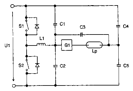
Figure 1 shows a half-bridge topology known per se
having two switching transistors S1 and S2. Said
switching transistors S1 and SZ lie in series between
two supply branches, between which an intermediate
circuit voltage U1 is applied. The intermediate circuit
voltage U1 can be generated by rectifying a system
voltage with corresponding filtering and, possibly,
power factor correction.
By means of an alternating switching operation of the
half-bridge transistors S1 and S2, a center tap between
them is switched to and fro between the potentials of
the supply branches. Correspondingly, a radiofrequency
AC potential corresponding to this switching operation
is applied to the left-hand connection of an inductor
L1 illustrated in figure 1. The inductor L1 is in series
CA 02503635 2005-04-06
-
with a high-pressure discharge lamp Lp, a block G1
connected therebetween representing a starting circuit
known per se. Said starting circuit generates a
starting pulse for starting the lamp Lp by means of
capacitor discharge and upward transformation in a
manner which is of no more interest to the invention.
The right-hand connection of the lamp Lp is connected
to the two supply branches via two coupling capacitors
C4 and C5. The coupling capacitors C4 and C5 ensure that
the right-hand connection of the lamp Lp has a
potential in the center between the potentials of the
supply branches. The circuit is thus able to generate
half the intermediate circuit voltage via the lamp Lp.
A filter capacitor C3 lies in parallel with the lamp
Lp. A tap between the lamp inductor L1 and the starting
circuit G1 is connected in each case to the supply
branches via two filter capacitors C1 and C2.
during actual operation of a high-pressure discharge
lamp, an operating voltage of an order of magnitude of
80 V - 150 V is required which is actually less than
half the intermediate circuit voltages which are
generally available. In this case, during a switching
phase in which, for example, the half-bridge transistor
S1 is conductive, said half-bridge transistor S1 is thus
interrupted in a clocked manner in order to generate,
together with the inductor L1, a step-down converter
operation during this switching phase. As a result, a
desired lamp operating voltage can be set by means of
the step-down converter operation.
On the other hand, a high-pressure discharge lamp
requires, for the transition from a glow discharge,
which follows on from the actual starting, to the arc
discharge, a certain period of time in which a transfer
voltage, which is markedly higher than the operating
voltage, in the range of, typically, 260 V - 330 V
needs to be provided. This value is generally above
half the intermediate circuit voltage. The half-bridge
CA 02503635 2005-04-06
_ g _
combined with the step-down converter cannot generate
this voltage without difficulty.
According to the invention, a resonance of a lamp
S resonant circuit, which comprises the capacitors C1 - C3
and the inductor L1, is excited during the transfer
phase. As a result, a voltage increase is induced, by
means of which the desired transfer voltage can be
generated. According to the invention, this resonance
excitation is, however, only used for the transfer
voltage and not for the starting voltage, with the
result that the filter capacitors can have a desired
size of, typically, 50 nF in the case of a ballast for
a 35 W lamp or 100 nF in the case of a ballast for a
70 W lamp, and corresponding capacitances for other
lamp powers. In fact, this desired size is the
effective total capacitance of the capacitors C1 to C3.
If, with this effective filter capacitance, resonance
starting were to take place, considerable currents
would be produced as a result of the starting voltages
required of an order of magnitude of 1.5 kV - 5 kV
together with said capacitance. The inductor L1 would
correspondingly have to be provided with very large
dimensions in order to be able to absorb the energy
correlating therewith. (This energy is proportional to
the filter capacitance and the square of the voltage.)
Such dimensions for the inductor are regarded as
unfavorable in accordance with the invention as regards
physical size and costs.
Although there is the possible solution of an increase
in the intermediate circuit voltage, this is associated
with disadvantages owing to the dimensions of the
components of the half-bridge and a possible power
factor correction circuit and also in terms of
efficiency.
CA 02503635 2005-04-06
- 10 -
Said resonance excitation for the purpose of generating
the transfer voltage takes place according to the
invention at lower frequencies than the resonant
frequency of the lamp resonant circuit, in this
exemplary embodiment approximately at half the resonant
frequency, to be precise at 0.55 times the resonant
frequency. Only moderate voltage increases thus result,
which are, however, fully sufficient for the transfer
phase. In particular, the position of the frequency
below the resonant frequency ensures that no
fundamental instabilities occur given any unintentional
saturation occurrences or other fluctuations. In
particular, it is thus possible to avoid a rapid
controller and a rapid voltage or current measurement
at the lamp resonant circuit.
Figure 2 shows a schematic illustration of the clocking
of the switching operation of the two transistors S1
and S2 shown in figure 1. The upper part represents the
upper transistor S1 (UGS1), and the lower part
represents the lower transistor S2 (UGS2). It can be
seen that in this case two cycles occur, to be precise
firstly a longer cycle between the pulse packets
(PerHB) and secondly a shorter cycle within the pulse
packets (PerSD). In terms of quality, this corresponds
to the combination already described comprising step
down converter operation and half-bridge operation, the
short cycle representing the step-down converter
operation and the longer cycle representing the half
bridge operation.
However, of concern here is the operation during the
transfer phase. The longer cycle in this case
represents near-resonance excitation at approximately
0.55 times the resonant frequency. Within the
corresponding conductive phase, represented by the high
level of the gate voltage of the corresponding
transistor, "chopping", i.e. modulation with the
shorter cycle duration, takes place. This is markedly
CA 02503635 2005-04-06
- 11 -
above the resonant frequency, but could in certain
cases also be less than the resonant frequency. It is
only necessary to avoid coming too close to the
resonant frequency. With "chopping", the effective
amplitude of the square-wave excitation can be reduced
to a certain extent at 0.55 times the resonant
frequency. Owing to "chopping" at a markedly higher
frequency, only the average value is relevant to a
certain extent for the resonant circuit. An addition or
alternative would otherwise consist in shortening the
switch-on phases with respect to half the time
component, i.e. to a certain extent to set the "chopper
pulses" synchronously at the start or the end of a
conductive phase.
Figure 3 shows a real graph relating to the ballast
circuit shown in figure 1. The uppermost waveform at
channel 1 shows the gate voltage of the lower half-
bridge transistor S2, the central waveform at channel 2
shows the potential of the half-bridge center point,
and the lower waveform at channel 3 shows the voltage
across the lamp.
The marked excursion of the lamp voltage approximately
at the end of the first box from the left shows
starting of the lamp with the aid of the starting
circuit G1. The radiofrequency resonance excited
thereby is of no further interest for the invention and
has to do with stray inductances in the starting
circuit G1 in connection with specific capacitances.
However, it can be seen that the "chopped" square-wave
switching operation (illustrated by figure 2) of the
half-bridge transistor is already present prior to
starting. Here, although no starting takes place and,
as a result, there is also no transfer, there is also
no damage. It is not necessary for synchronization with
the starting process to take place. Rather, the
depicted "chopped" half-bridge operation ensures near-
resonance (0.55 times the resonant frequency)
CA 02503635 2005-04-06
- 12 -
excitation with a corresponding voltage increase across
the lamp. In the present case, as is shown in figure 3,
voltage amplitudes across the lamp of almost ~ 400 V
result. This excitation takes place with the AC voltage
illustrated at channel 2 at the bridge center point.
Not only the "chopper operation" of the lower switching
transistor SZ but also, in the switching phases
therebetween, the "chopper operation" of the upper
switching transistor S1 can be seen there. It can also
be seen that in each case only the first two gate
voltage drops have an influence on the voltage at the
bridge center point. This is associated with the
freewheeling diodes which can be seen in figure 1 and
which are connected in parallel with the switching
transistors S1 and S2. Depending on the sign of the
inductor current through the inductor L1, the latter
carry the current such that the modulation of the gate
voltage remains without effect.
Typical resonant frequencies are approximately
20 kHz.- 40 kHz. In the present case, the effective
total capacitance of the filter capacitors is 100 nF,
and the inductance of the inductor L1 is 500 uH. The
fundamental excitation frequency is 12.5 kHz, and the
resonant frequency is approximately 22.5 kHz.
It can be seen from the lamp voltage on channel 3 that,
at the transition from the conductive switching phase
of one switching transistor to the conductive switching
phase of the other switching transistor, approximately
a sinusoidal cycle of the lamp voltage begins. In this
case, the two shoulders between the extreme values of
the lamp voltage correspond to the start and to the end
of such sinusoidal cycles, i.e. approximately to the
extremes of the individual sinusoidal period. They are
step responses to the resonance excitation as a result
of the excitation frequency which is markedly lower
than the resonant frequency. In this case, the lamp
voltage oscillates at double the excitation amplitude
CA 02503635 2005-04-06
- 13 -
and would then carry out a sinusoidal oscillation about
the excitation amplitude, of which, however, only a
first section can be seen. This is based precisely on
the ratio, which approximately corresponds to the
number 2, between the excitation frequency and the
resonant frequency.
The level of the transfer voltage can thus be set
firstly by selecting the excitation frequency, secondly
by the "chopper operation", and thirdly naturally by
the temporal length of the conductive phases of the
switching transistors.
Figure 3 shows the fact that the "chopper frequency"
corresponds approximately to eight times the
fundamental excitation frequency. In this case, a duty
cycle is achieved within the modulation frequency, i.e.
a ratio between the switch-on phase and the associated
switch-off phase by "chopping", of approximately 850
(the duty cycle is only based on the modulation and not
on the basic clocking).