Note: Descriptions are shown in the official language in which they were submitted.
CA 02503752 2005-04-04
2003PI4669U5-RAI
Electronic ballast with regulating circuit and
disturbance variable application
Field of the invention
The present invention relates to an electronic ballast
for lamps, in particular but not exclusively low-
pressure discharge lamps.
Background of the invention
Such ballasts usually contain a rectifier that
rectifies an AC supply voltage in order to generate an
intermediate circuit voltage. This intermediate circuit
voltage is usually present on an intermediate circuit
capacitor for smoothing or storage. The intermediate
circuit voltage supplies a converter, for example a
half-bridge oscillator, which for its part generates
the supply power fox the lamp, a radiofrequency supply
power in the case of a low-pressure discharge lamp, but
also a DC voltage that alternates in polarity at a
comparatively low frequency in the case of a high-
pressure discharge lamp.
It is furthermore known to provide, in such ballasts,
regulating circuits by means of which the lamp current
or the lamp power is regulated to a constant value. It
is thus possible to compensate for drift effects as a
result of lamp aging, temperature changes and the like.
Summary of the invention
The present invention is based on the technical problem
of specifying an improved electronic ballast with a
regulating circuit.
The invention relates to an electronic ballast for a
lamp having a rectifier for generating a rectified
~
' CA 02503752 2005-04-04
- 2 -
intermediate circuit voltage, a converter for
generating a supply power for the lamp, a control for
the forced control of the converter and a regulating
circuit for regulating the lamp current or the lamp
power, which is designed to influence the control of
the converter, characterized in that the ballast is
designed to the effect that the control of the
converter is also influenced by a disturbance variable
application that takes account of fluctuations of the
rectified intermediate circuit voltage.
The invention furthermore relates to a corresponding
method.
The basic idea of the invention is as follows: in the
course of rectifying the supply power, a residual
modulation of the intermediate circuit voltage remains,
in principle. This modulation influences the converter
and thus the operation of the lamp. Although such a
modulation can also be corrected in the case of a
regulating circuit known per se, the inventor has
ascertained that the intermediate circuit voltage
modulation is comparatively fast in comparison with
other disturbance variables such as lamp aging,
temperature changes and the like and primarily in many
cases is the only fast disturbance variable in this
sense. Since the modulation behavior of the
intermediate circuit voltage in the case of a known
rectifier and a given intermediate circuit capacitor is
relatively constant in the sense of predictable or
calculable, the invention proposes taking account of
the modulation of the intermediate circuit voltage as a
disturbance variable in the context of a disturbance
variable application outside the actual regulation
feedback. This affords the advantage that the
regulating circuit can be designed for significantly
slower operation and the necessary measurements, for
instance the lamp current measurement, can also be
carried out correspondingly slowly. The feedback
. ' CA 02503752 2005-04-04
- 3 -
control loop thus becomes less demanding and the
disturbance variable that is conventionally the cause
of a relatively fast regulation is "excluded" and taken
into account separately by means of the disturbance
variable application. In this case, the disturbance
variable application means "computationally" taking
into account in the sense of - as a rule proportionally
- taking into account the deviation of the disturbance
variable from a nominal value in the case of the
control of the converter.
A relatively slow I regulator may preferably be used,
which is simple to realize and operates well in the
case of slow regulations. It has the advantage,
moreover, of not permitting a permanent regulating
deviation.
Furthermore, it is preferred for the regulating circuit
to be embodied digitally. A digital regulating circuit
requires a limited technical outlay in any event when
no stringent requirements are made of speed. Moreover,
it is well suited to integration - which is preferred
in the context of the invention - into a likewise
digital control circuit, which is preferably realized
by a microcontroller, that is to say a programmable IC.
The regulating circuit can then therefore be realized
essentially by software technology. In such cases in
which, therefore, a digital circuit, in particular a
microcontroller, is provided anyway for reasons
independent of the regulation, the outlay required for
the digital regulating circuit is significantly lower
than that for a conventional analog regulating circuit.
Here, too, the outlay can be significantly reduced in
the case of minor speed requirements.
The ballast according to the invention preferably has a
so-called power factor correction circuit, that is to
say a circuit that provides for an as far as possible
sinusoidal power consumption from the AC voltage mains.
. ' CA 02503752 2005-04-04
- 4 -
It is thus possible to avoid the pulsed current spikes
that arise, in the event of simple charging of the
intermediate circuit capacitor with a rectifier, when
the mains voltage rises above the instantaneous
intermediate circuit voltage. A preferred example of
such a power factor correction circuit (also referred
to as PFC circuit) are a so-called step-up converter
(boost converter) and a so-called SEPIC converter,
which are known per se.
The control of the power factor correction circuit
requires a measurement of the intermediate circuit
voltage anyway, so that the invention requires a
particularly low additional outlay in such cases. In
this case, the control of the power factor correction
circuit is preferably likewise integrated in the
digital control circuit.
Brief description of the drawings
The invention is explained in more detail below on the
basis of a schematic exemplary embodiment, in which
case the individual features may also be essential to
the invention in other combinations. In particular it
is expressly established once again that the invention
has both a device character and a method character and
the description above and also the description below
implicitly relate to both aspects.
Figure 1 shows a schematic block diagram of an analog
regulating circuit in a conventional ballast.
Figure 2 shows, in comparison with figure 1, a digital
regulating circuit with disturbance variable
application in a ballast according to the
invention.
Figure 3 shows a schematic block diagram of an
electronic ballast according to the invention
' CA 02503752 2005-04-04
- 5 -
with a digital regulating circuit according
to figure 2.
Detailed description of the invention
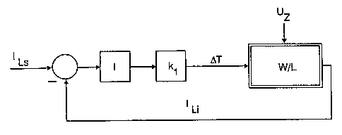
Figure 1 shows a fast analog regulator for regulating
the lamp current of a low-pressure discharge lamp
according to the prior art. In figure 1, W/L designates
a converter, here a half-bridge oscillator, with a
connected low-pressure discharge lamp L. The signal
line leading into the block W/L is designed by DT,
which symbolizes that the switching times or the period
duration of converter operation are set here. The
signal line leading out of the block W/L is designated
by ILi, which symbolizes that the lamp current through
the lamp L is measured here. It can be seen in the
left-hand region of figure 1 that the measured "actual"
lamp current IL;, is compared with a desired current
value ILS by means of a comparator. The desired value
deviation is fed to a fast analog integral regulating
element designated by I. The output signal of the
integral regulating element I is multiplied by a
specific factor kl and, as already mentioned, used for
setting the period duration T of converter operation.
If the integral regulating element I outputs a zero
signal, the period duration remains the same.
Therefore, the signal line to the block W/L is
designated by 0T in the sense of a period duration
change.
A further "signal" that passes into the block W/L in
accordance with figure 1 is the intermediate circuit
voltage UZ. This symbolizes that converter operation
and lamp operation, and also in particular the lamp
current ILi are dependent on the intermediate circuit
voltage UZ and, in particular, are subjected to the
modulations thereof. The conventional control loop
illustrated in figure 1 must therefore be fast enough
to correct the intermediate circuit voltage modulation
-' CA 02503752 2005-04-04
- 6 -
with a typical frequency of 100 Hz. In the case of
high-quality electronic ballasts, the modulation of the
lamp current or the lamp power must not exceed specific
limits.
An alternative or else accompanying measure consists in
choosing the intermediate circuit capacitor to be large
enough in order to keep the intermediate circuit
voltage modulation inherently small. However; a Large
intermediate circuit capacitor is associated with
additional costs and, moreover, increases the switch-on
current of the ballast.
Figure 2 shows the invention in comparison with
figure 1. In this case, the same reference symbols are
used for corresponding parts. The following description
concentrates on the differences.
Firstly, the intermediate circuit voltage is designated
here by the symbol UZi. In contrast thereto, UZ$
designates an intermediate circuit voltage desired
value. The intermediate circuit voltage actual value
(measured value) UZi is compared with the intermediate
circuit voltage desired value UZS by means of a
comparator, multiplied by a constant k2 and added to
the output of the integral regulating element I
multiplied by the constant kl as already described with
reference to figure 1, in order to influence the period
duration of converter operation in the manner already
described. The constants kl and k2 permit an adaptation
of the behavior.
The unit - designated by the symbol SG - comprising the
comparator for comparing the intermediate circuit
voltage actual value UZi with the intermediate circuit
voltage desired value UZg and the kz multiplication thus
forms a disturbance variable application to the control
loop which, for the rest, corresponds in principle to
figure 1.
.' CA 02503752 2005-04-04
_ 7 _
However, with the disturbance variable application SG,
the intermediate circuit voltage modulation can be
taken into account relatively rapidly in a sufficiently
precise manner and primarily without a technical
outlay. Therefore, in the case of the control loop
according to figure 2, the lamp current ILi does not
have to be measured rapidly. Furthermore, the integral
regulating element I can be slow. This is because the
control loop now only has the task of correcting
changes in converter and lamp operation that take place
relatively slowly with respect to time.
The arrangement described in figure 2 is part of a -
for the rest - conventional electronic ballast for
supplying a low-pressure discharge lamp L. Figure 3
shows a block diagram in this respect. The intermediate
circuit voltage UZi is generated by means of a
conventional diode bridge rectifier with customary
filter elements for preventing radiofrequency
components from being fed back into the mains,
designated by FR in figure 3. A power factor correction
circuit is employed here, in this case a boost
converter with the switching transistor T3, the
inductance L1, the diode D1 and the storage capacitor
Cl for the intermediate circuit voltage Uzi. For the
control of the switching transistor T3 of the boost
converter, the intermediate circuit voltage UZi has to
be measured anyway, which is illustrated in figure 3 by
the tap at the voltage divider circuit (not
specifically designated). In the case of this exemplary
embodiment, this measurement is simultaneously used for
the disturbance variable application illustrated in
figure 2. Moreover, the disturbance variable
application, the control loop, the control of the half-
bridge oscillator W and the control of the boost
converter are realized jointly by software technology
in a digital microcontroller uC. The half-bridge
oscillator W has the two switching transistors T1 and
CA 02503752 2005-04-04
T2 from figure 3 and supplies the lamp circuit - which
is connected up in a customary manner and not explained
in any greater detail here - with the lamp L at the
center tap between the switching transistors T1 and T2
with a supply voltage oscillating at high frequency.
The microcontroller uC measures, in the manner
indicated in figure 3, the current through the lamp L
and the current through the lower switching transistor
T2 in order to correspondingly drive the half-bridge
oscillator W. .