Note: Descriptions are shown in the official language in which they were submitted.
CA 02503825 2005-04-26
WO 2004/042458 PCT/US2003/034577
AN INTEGRATED OPTIC POLARIZATION CONVERTER BASED ON
STRUCTURAL CHIRALITY
PRIORITY INFORMATION
This application claims priority from provisional application Ser. Nos.
60/422,414 filed October 30, 2002, and 60/478,751 filed June 16, 2003, which
are
incorporated herein by reference in their entirety.
BACKGROUND OF THE INVENTION
The invention relates to the field of integrated optic polarization
converters,
and in particular to integrated optic polarization converters based on mode
evolution
or structural chirality.
As the prevalence of fiber optic communication grows, the demand for more
intricate processing of optical signals continues to increase. Since
integrated optic
devices allow for integration of many optical functions on a chip, integrated
optic
approaches will likely fill the demand for more intricate optical signal
processing.
However, in order to improve the functionality and reduce the cost per
function the
density of components on the chip must increase.
For a given wavelength, the confinement of a mode in a dielectric waveguide
is determined by the contrast between the core and cladding indices, the
higher the
contrast, the tighter the confinement. An outgrowth of tighter confinement is
the
ability to pack waveguides closer together and guide light around sharper
bends
without substantial radiative loss. Since these are the two most critical
parameters
affecting device density, it can generally be said that the higher the index
contrast
the greater the device density. However, as the index contrast increases, the
transverse electric (TE) and transverse magnetic (TM) modes propagating in the
waveguides begin to exhibit different characteristics. While in a straight
section of a
square waveguide, the TE and TM modes propagate at the same rate, in a bend
the
TE and TM modes propagate at substantially different rates. And, when a pair
of
square high index contrast (HIC) guides is coupled, the TE and TM modes tend
to
couple at different rates. Since most integrated optic components are
sensitive to
both propagation velocity and guide-to-guide coupling, these effects result in
CA 02503825 2005-04-26
WO 2004/042458 PCT/US2003/034577
l
polarization dependent performance, a result that is not compatible with the
random
polarization state emanating from the standard single mode fiber used in
telecom
applications.
One way to compensate these effects is to use a rectangular waveguide
S geometry and alter the aspect ratio of the guide to compensate for the
natural
difference in propagation around a bend and/or equalize the guide-to-guide
coupling. However, while one or the other of these effects may be compensated
in
this manner for a particular device, as the index contrast increases it
becomes
difficult if not impossible to compensate both simultaneously in a manner that
applies to all devices on the chip.
Another approach for overcoming the polarization sensitivity of HIC
integrated optics is to split the random input polarization emanating from the
single
mode (SM) fiber with a polarizing beam splitter (PBS), couple the outputs to
polarization maintaining (PM) fibers, twist one of these PM fibers by
90° degrees
1 S and couple the two fibers to separate paths on the integrated optic chip.
On each of
these paths identical structures are used to process the two components
independently. At the output, these components are recombined by coupling to
another pair of PM fibers, twisting the PM fiber of the path that had not
previously
been twisted and coupling both fibers to another PBS which has a SM fiber
output.
While such an approach, commonly referred to as a "polarization diversity"
scheme, is feasible, when implemented with bulk optics it is also cumbersome.
Aligning PM fibers is difficult and expensive. And, in order to preserve
signal
integrity the path lengths must be matched to within at least one-tenth of a
bit length
(i.e. -~mm for lOGb/s signals and -0.Smm for 40Gb/s signals assuming an index
of
1.5).
A better approach is to integrate the splitting function of the PBS and the
rotating function of the twisted PM fiber onto the integrated optic chip.
Doing so
would eliminate the need to align PM fibers and path lengths could be matched
easily through lithography.
Several integrated optic polarization splitters and rotators (or converters)
have been proposed. However, most of the devices proposed to date rely on the
coupling of a pair of waveguide modes. Devices based on coupled modes
generally
CA 02503825 2005-04-26
WO 2004/042458 PCT/US2003/034577
3
exhibit a wavelength sensitivity resulting from differences in the dispersion
of the
super-modes propagating in the structure. Further, such approaches are very
sensitive to fabrication errors. Even slight changes in the waveguide
geometries or
separation can have a significant impact on the device performance.
A better way to form a polarization splitter or rotator is to use the
principle
of mode evolution. By making gradual (or adiabatic) changes to the waveguide
geometry, the modes in the guide can be conditioned and the polarization
states
separated or rotated. Such an approach only requires that the modes not
exchange
power which can be assured by proper design of the waveguide and a slow
evolution
of the structure. Since prevention of mode coupling is a relatively loose
requirement, devices based on mode evolution tend to be wavelength insensitive
and
fabrication tolerant. It has been proposed and demonstrated that a
polarization
splitter based on mode evolution can be formed, however, this approach has the
disadvantage of requiring multiple waveguide materials. And, to date no
polarization converters have been proposed which utilize the principle of mode
evolution.
Generally, it is the object of the invention to convert a TM input
polarization
to a TE output polarization or vice versa with an integrated optic device
based on
the principle of mode evolution or structural chirality.
It is yet another object of the invention that the device be wavelength
insensitive, tolerant to fabrication errors, and require only a single
material system
to construct.
These and other objects of the present invention will become apparent to
those skilled in the art from the following detailed description and
accompanying
figures.
SUMMARY OF THE INVENTION
According to one aspect of the invention, there is provided an integrated
optic polarization converter. The integrated optic polarization converter
includes a
plurality of core layers used to approximate a gradually twisted waveguide and
therein adiabatically transform a propagating mode from an initial
polarization state
to a different final polarization state.
CA 02503825 2005-04-26
WO 2004/042458 PCT/US2003/034577
4
According to another aspect of the invention, there is provided a method of
forming an integrated optic polarization converter. The method includes
receiving
an initial polarization state. Also, the method includes forming a plurality
of core
layers to approximate a gradually twisted waveguide and therein adiabatically
transform a propagating mode from the initial polarization state to a
different final
polarization state.
BRIEF DESCRIPTION OF THE DRAWINGS
FIG. 1 is a schematic diagram of a twisted waveguide;
FIG. 2 is a schematic diagram of a polarization converter using three
adiabatically tapered core layers;
FIGS. 3A-3B are grayscale images of the fundamental mode electric field
propagating in the waveguide of the invention;
FIG. 4 is a graph demonstrating the performance of a particular
implementation of the device in FIG. 2 as a function of the device length;
FIG. S is a graph demonstrating the performance of a particular
implementation of the device in FIG. 2 as a function of the wavelength of the
electromagnetic field;
FIG. 6 is a schematic diagram of a polarization converter using three
adiabatically tapered and separated core layers;
FIG. 7 is a schematic diagram of a polarization converter using adiabatic
tapering of the middle layer and adiabatic separation of the upper and lower
core
layers;
FIG. 8 is a graph demonstrating the performance of a particular
implementation of the device in FIG. 7 as a function of the device length;
FIG. 9 is a graph demonstrating the performance of a particular
implementation of the device in FIG. 7 as a function of the wavelength of the
electromagnetic field;
FIG. 10 is a schematic diagram of a polarization converter using only two
layers that are adiabatically tapered and separated;
FIG. 11 is a graph demonstrating the performance of a particular
implementation of the device in FIG. 10 as a function of the device length;
and
CA 02503825 2005-04-26
WO 2004/042458 PCT/US2003/034577
FIG. 12 is a graph demonstrating the performance of a particular
implementation of the device in FIG. 10 as a function of the wavelength of the
electromagnetic field;
5 DETAILED DESCRIPTION OF THE INVENTION
The mode structure for a general rectangular dielectric waveguide consists of
a minimum of two guided electromagnetic modes, a TE (or quasi-TE) mode and a
TM (or quasi-TM) mode, and an infinite sum of unguided (or radiation)
electromagnetic modes. If a rectangular waveguide is rotated by 90°,
its mode
structure is similarly rotated with the TE mode becoming the TM mode and vice-
versa. Therefore, a smooth transition between a rectangular waveguide and its
rotated counterpart should enable polarization conversion through mode
evolution.
However, any perturbation to the initial structure will induce coupling
between the
modes. For a mode evolution approach to work, power exchange between the
modes must be inhibited.
A way to transition between a rectangular waveguide and its rotated
counterpart is to twist the initial structure. FIG. 1 is a schematic diagram
of an
adiabatically twisted dielectric waveguide 100 having an input 102 and output
104.
The twisting of the waveguide 100 acts as a perturbation to the mode structure
of the
rectangular guide inducing coupling amongst the guided modes and between the
guided modes and radiation modes. Since coupling between guided and radiation
modes requires strong perturbations, coupling to radiation modes can generally
be
ignored in slowly evolving structures. However, coupling amongst the guided
modes remains an important effect.
If the waveguide 100 in FIG. 1 were square, the guided modes would be
degenerate and therefore propagate at the same rate. The field coupling
induced by
the twist would add coherently along the length of the structure and the power
exchange between the modes would be substantial. This would be an undesirable
result, as the twisted waveguide 100 is meant to work on the principle of mode
evolution rather than mode coupling. To inhibit the coupling, a rectangular
waveguide with a large aspect ratio is used so that the guided modes will
propagate
at different rates. In this case, the power coupled from one mode to the other
along
CA 02503825 2005-04-26
WO 2004/042458 PCT/US2003/034577
6
the length of the structure will add incoherently as long as the structure is
sufficiently long to allow the modes to de-phase. As the index contrast,
aspect ratio,
and length of the transition increase, the degree of incoherence also
increases and
the accumulated power exchange along the length of the structure can be made
arbitrarily low. The performance departs from ideality only when the
transition
becomes too short or the aspect ratio of the guide too small to allow for de-
phasing
to occur.
The structure 100 in FIG. 1 is an ideal structure with a perfect twist of the
waveguide. However, for practical implementation of the device all such
geometries should be formed from micro-fabrication techniques, which generally
require the structures be formed from a layering process with features defined
through lithography. It is therefore desirable to approximate this twisted
waveguide
with a finite number of layers. Herein, a layer is defined as a horizontal
slice
through the waveguide cross-section which contains no variations of refractive
index
in the vertical direction.
An optical waveguide is typically formed by dielectric materials of various
refractive indices. Generally, the higher index materials are considered core
materials while the lower index materials are considered cladding materials.
To be
specific, a cladding material is herein defined as the material of lowest
refractive
index within a layer. All other materials within the layer are therefore core
materials. A core layer is defined as a layer containing a core material.
The basic requirements for the structure to operate as a polarization
converter are quite loose, with the primary requirement being that the
structural
chirality, or twist in the electromagnetic sense, be preserved. A few of the
possible
geometries are described below.
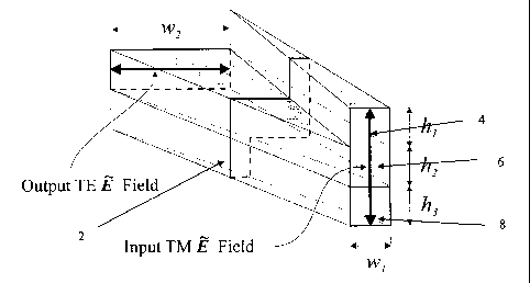
FIG. 2 is a schematic diagram of an integrated optic polarization converter 2
using three core layers 4, 6, and 8 with heights h,, hz, and h3, respectively,
to
approximate a twisted waveguide and transform the structure from a vertically
aligned rectangular waveguide to a horizontally aligned rectangular waveguide.
In
the described embodiment, each of the layers 4, 6, and 8 have a width of w, at
the
input. At the output of the structure 2 the waveguide width is wz, which is
approximately equivalent to the sum of the heights hl, h2, and h3. The height
at the
CA 02503825 2005-04-26
WO 2004/042458 PCT/US2003/034577
7
output is that of the middle layer hz. However, the geometry of the structure
may
vary depending on the requirements of the application.
A cladding, with a lower refractive index than the core layers, is typically
arranged around the core layers to provide light confinement.
The transition is achieved by removing material from the upper 4 and lower
8 core layers and adding material to the middle core layer 6 in a manner
approximating a rotation of the waveguide axis.
FIGs. 3A-3B are grayscale images of the fundamental mode field
propagating in the inventive waveguide. FIG. 3A depicts a grayscale image of
the
x component of the fundamental mode electric field profile for the starting
10,
middle 12 and ending 14 structures. FIG. 3B depicts a grayscale image of the y
component of the fundamental mode electric field profile for the starting 16,
middle
18 and ending 20 structures.
From the mode profiles, it is shown that the mode is initially polarized along
the y direction, but mid-point along the structure the mode field components
are
somewhat evenly split, and at the end of the structure the mode is polarized
primarily along the X direction. Coupled local mode theory dictates that an
adiabatic transition between these structures enables mode conversion from the
y
polarized state in the initial guide to the x polarized state in the final
guide 2. Since
both the primary and secondary modes are transformed, the inverse is also
true.
That is a X polarized state in the initial guide will generally be transformed
to a y
polarized state in the final guide. Additionally, the principle of reciprocity
ensures
that the device operates in reverse. That is, x and y polarized states
starting from
the end of the structure will be adiabatically transformed into y and x
polarized
states at the beginning of the structure, respectively.
FIG. 4 is a graph demonstrating the performance of a particular
implementation of the converter depicted in FIG. 2 as a function of the
structure
length. In this embodiment, h, = h2 = h3 = w, = 0.25 ~.m, w2 = 0.75 ~.m, the
core index is 2.2 and the cladding index is 1.445, and the transition is
linear along
the direction of propagation z , however, in other embodiments these
parameters
can vary and non-linear transitions may be utilized. A three-dimensional mode
scattering formulation was used to perform the simulation and the wavelength
CA 02503825 2005-04-26
WO 2004/042458 PCT/US2003/034577
g
considered was 1.55 pin. Mode scattering simulations are a particularly
accurate
modeling tool when only a few modes per waveguide cross-section are required
to
represent the system. Since the radiation modes do not substantially influence
the
operation of approaches based on mode evolution, the mode-scattering technique
is
well suited for these problems. Additionally, the results presented were
confirmed
at a few device lengths with full three dimensional finite difference time
domain
(FDTD) simulations. The FDTD method is a complete numerical implementation of
Maxwell's Equations. The results of the mode scattering simulation presented
in
FIG. 4 show that 99 % or more of the power is transferred successfully from a
TM
polarization to a TE polarization with taper lengths of only a couple hundred
microns. As was hypothesized for a guide with a pure twist, it is found that
when
the taper is too short, and thus the perturbation too strong to allow for the
modes to
de-phase, the guided modes exchange power and the device performance degrades
leaving power in the TM polarized state.
FIG. 5 is a graph demonstrating the broadband performance of the particular
embodiment considered in FIG. 4 when the device length is set to 200 pin. Here
again, a three-dimensional mode scattering formulation was used to perform the
simulation. FIG. 5 shows that no wavelength sensitivity is discernable over
the
entire 1.45 pin to 1.65 pin regime; a wavelength span of interest for
telecommunications. The broadband performance of the approach is consistent
with
the underlying theory of operation. Since the aim is to transition modes from
one
state to another without introducing coupling amongst the modes, the bandwidth
is
only limited by the extent to which the coupling amongst the modes is
increased at
one wavelength relative to another. At short wavelengths the appearance of
additional modes may facilitate this coupling and at long wavelengths the
modes
become more closely phase-matched thereby reducing the primary effect, which
inhibits coupling between the modes. In either case, large changes in
wavelength
are required for these phenomena to take effect. This is in contrast to
approaches
based on coupled modes that suffer from an inherent bandwidth limitation
associated
with differences in the dispersion of the super-modes.
Many variations of the basic structure are possible. Both the geometry and
refractive indices may differ from the particular embodiment described.
CA 02503825 2005-04-26
WO 2004/042458 PCT/US2003/034577
9
FIG. 6 is a schematic diagram of another embodiment of the inventive
polarization converter 24. Fabrication limitations may prevent the upper 26
and
lower 28 layers from reaching infinitesimal widths smoothly. Therefore, it may
be
advantageous to consider structures where the final transition is handled by
separating the upper 26 and lower 28 layers from the middle layer 30, as shown
in
FIG. 6. This results in a nearly equivalent adiabatic transition to the final
output
waveguide.
The structure 24 is designed so that initially the upper layer 26, middle
layer
30, and lower layer 28 will have heights of h,, h2, and hj respectively.
Moreover,
each of the layers 26, 28, and 30 will have a width of w, at the input. Note
at the
output of the structure 24 the width is wz, which is approximately equivalent
to the
sum of the heights h,, h2, and h3. The height at the output is that of the
middle layer
h2.
A cladding, with a lower refractive index than the core layers, is typically
arranged around the core layers to provide light confinement.
FIG. 7 is a schematic diagram of another embodiment of the inventive
polarization converter 32 similar in nature to that of FIG. 6. However, here
the
upper 34 and lower 38 layers are in fact not tapered at all, but rather
gradually
separated from the middle layer 36. In this manner the minimum feature size
can be
made even larger thereby further facilitating the ease of fabrication. The
upper 34
and middle 36 layers are separated at the output by a distance s, and the
middle 36
and lower 38 layers are separated at the output by a distance s.
The structure 32 is designed so that initially the upper layer 34, middle
layer
36, and lower layer 38 will have heights of h,, h2, and h3 respectively.
Moreover,
each of the layers 34, 36, and 38 will have a width of w,. Note at the output
of the
structure 32 the width is wz, which is approximately equivalent to the sum of
the
heights h,, h2, and hj. The height at the output is that of the middle layer
hz.
A cladding, with a lower refractive index than the core layers, is typically
arranged around the core layers to provide light confinement.
FIG. 8 is a graph demonstrating the performance of a particular embodiment
of the polarization converter depicted in FIG. 7 as a function of the
structure length.
In this embodiment, the parameters were set as follows h, = hz = h3 = 0.25pm,
w,
CA 02503825 2005-04-26
WO 2004/042458 PCT/US2003/034577
= 0.25 pm, w2 = 0.75 pm, s = 0.125 p,m and the core and cladding indices are
2.2 and 1.445, respectively. In other embodiments, these parameters can vary.
Again, a three-dimensional mode scattering formulation was used to perform the
simulation and the wavelength considered was 1.55 pm. Performance similar to
S that of the original embodiment is obtained with device lengths of only a
couple
hundred microns.
FIG. 9 is a graph demonstrating the broadband performance of the particular
embodiment considered in FIG. 7 when the structure length is set to 100 pm.
Here
again, a three-dimensional mode scattering formulation was used to perform the
10 simulation. FIG. 5 shows that no wavelength sensitivity is discernable over
the
entire 1.45 pm to 1.65 p.m regime.
Although three layers are the minimum required for the device to be
symmetric, any of the aforementioned approaches may be applied to a device
composed of only two core layers. FIG. 10 is a schematic diagram of a
polarization
converter 40 using only two core layers 42, 44. In this embodiment, the upper
42
and lower 44 layers are both tapered and separated simultaneously.
The polarization converter 40 is designed so that initially the upper layer 42
and lower layer 44 will have heights of h, and h2, respectively. Moreover,
each of
the layers 42 and 44 will have a width of w, at the input. At the output, the
width of
the upper layer is w3. Note that at the output of the chiral waveguide
structure 40
the width is w2, which is approximately equivalent to the sum of the heights
h, and
hz. The height at the output is that of the middle layer h2. The performance
of the
device is unaffected by the ordering of the layers (i.e. which layer sits on
top).
A cladding, with a lower refractive index than the core layers, is typically
arranged around the core layers to provide light confinement.
FIG. 11 is a graph demonstrating the performance of a particular
embodiment of the structure depicted in FIG. 10 as a function of the structure
length. In this embodiment, the parameters are set as follows; h, = h2 = 0.4
pm, w,
= 0.4 pm, w2 = 0.8 pm, w3 = 0.25 pm, s = 0.25 pm, and the core and cladding
indices are 2.2 and 1.445, respectively. In other embodiments, these
parameters
can vary. Again, a three-dimensional mode scattering formulation was used to
perform the simulation and the wavelength considered was 1.55 pm. Despite the
CA 02503825 2005-04-26
WO 2004/042458 PCT/US2003/034577
11
asymmetry inherent to the two layer embodiment, the structure performs quite
well
with over 99 % of the power transferred from the TM polarization to the TE
polarization for structures of only a couple hundred microns in length.
FIG. 12 is a graph demonstrating the broadband performance of a 100 ~m
long implementation of the embodiment used for the simulation in FIG. 11.
Again,
a three-dimensional mode scattering formulation was used to perform the
simulation. FIG. 12 shows that no wavelength sensitivity is discernable over
the
entire 1.45 ~m to 1.65 pm regime.
Although the present invention has been shown and described with respect to
several preferred embodiments thereof, various changes, omissions and
additions to
the form and detail thereof, may be made therein, without departing from the
scope
of the invention.
What is claimed is: