Note: Descriptions are shown in the official language in which they were submitted.
CA 02503826 2005-04-26
WO 2004/040357 PCT/US2003/034404
POWER MANAGEMENT FOR SPATIAL POWER COMBINERS
BACKGROUND OF THE INVENTION
1. Field of the Invention
This invention relates to spatial power combiners, such as quasi-optic grid
arrays, and in particular to architectures for efficiently removing heat
generated by,
and supplying bias to, spatial power combiners.
2. Description of Related Art
Broadband communications, radar and other imaging systems require the
generation and transmission of radio frequency ("RF") signals in the microwave
and
millimeter wave bands. In order to efficiently achieve the levels of output
transmission power needed for many applications at these high frequencies, a
technique called "power combining" has been employed, whereby the output power
of individual components are coupled, or combined, thereby creating a single
power
output that is greater than an individual component can supply.
Conventionally,
power combining has used resonant waveguide cavities or transmission-line feed
networks. These approaches, however, have a number of shortcomings that become
especially apparent at higher frequencies. First, conductor losses in the
waveguide
walls or transmission lines tend to increase with frequency, eventually
limiting the
combining efficiency. Second, these resonant waveguide cavities or
transmission-line
combiners become increasingly difficult to machine as the wavelength gets
smaller.
Third, in waveguide systems, each device often must be inserted and tuned
manually.
This is labor-intensive and only practical for a relatively small number of
devices.
Several years ago, "spatial power-combining" was proposed as a potential
solution to these problems. In spatial power-combining, the individual outputs
of
microwave and millimeter wave solid-state devices combine in free space to
provide a
single combined power output more effectively than can ostensibly be achieved
using
the above-described conventional power-combining techniques.
As used herein, the term "spatial power-combining" broadly applies to all
structures that couple component outputs in free space. A subset of spatial
power-
combining that has recently received significant attention is called "quasi-
optical
power combining." The theory underlying "quasi-optics" is that an array of
1
CA 02503826 2005-04-26
WO 2004/040357 PCT/US2003/034404
microwave or millimeter-wave solid state sources placed in a resonator could
synchronize to the same frequency and phase, and their outputs would combine
in free
space, thus minimizing conductor losses. Furthermore, monolithic fabrication
enables
potentially thousands of microwave or millimeter wave active devices to be
incorporated on a single wafer.
Since then, numerous quasi-optical devices have been developed, including
detectors, multipliers, mixers, and phase shifters. These passive devices
continue to
be the subject of ongoing research. Over the past few years, however, active
quasi-
optical devices, namely oscillators and amplifiers, have evolved. One benefit
of
spatial power combining (over other methods) using quasi-optics is that the
output
power scales linearly with chip area. Thus, the field of active quasi-optics
has
attracted considerable attention in a short time, and the growth of the field
has been
explosive.
A quasi-optical array amplifier includes a two-dimensional sheet of active
devices, interconnected with patterned conductors, that accepts a polarized
electromagnetic wave as an input and radiates an amplified output wave with a
polarization that is orthogonal to the input polarization. Two array amplifier
configurations that have been previously reported are transmission-mode arrays
and
reflection-mode arrays. FIG. 1 shows a typical transmission-mode grid
amplifier 10,
wherein an array of closely-spaced interconnected differential pairs of
transistors 14
are formed in a grid-like pattern on the front surface of a semiconductor chip
12. The
chip is sandwiched between an input polarizer 18 and an output polarizer 24.
An
input signal 16 passes through the horizontally polarized input polarizer 18
and
creates an input beam incident from the left that excites if currents on the
horizontally-patterned, polarized, metal input antennas 20 of the grid on the
chip 12.
These currents drive the inputs of the transistor pairs 14 in the differential
mode. The
output currents are redirected along the grid's vertically-patterned polarized
antennas
22, producing, out the right side of the array, a vertically polarized output
beam 30 via
an output polarizer 24.
Reflection-mode arrays also use two-dimensional active grids similar to the
active grids in transmission mode arrays. However, reflection-mode arrays
require
that the EM radiation have access to only the front (active grid) surface of
the chip.
2
CA 02503826 2005-04-26
WO 2004/040357 PCT/US2003/034404
The back surface of the chip is mounted on a dielectric substrate atop a
.metallic
mirror.
Unfortunately, drawing heat away from quasi-optical arrays and, more
generally, from any type of spatial power combiners remains a problem,
especially for
high-power, high-frequency applications. In microwave and millimeter wave
semiconductor devices, heat is generated in the circuitry fabricated on the
front (or
top) surface of the semiconductor. In conventional microwave and millimeter
wave
circuits, in order to enhance heat removal, the semiconductor wafer is
typically
thinned to a final thickness of 50 to 150 microns. Further, the baclc (or
bottom)
surface of the semiconductor chip is completely covered with a metal "ground
plane,"
which acts as an equipotential shield and return conductor to the power
supply, that is
electrically connected to the devices on the front surface through metallic
"vial."
Additionally, this metal layer provides both a mechanical support as well as a
surface
for soldering devices to a metalized carrier, thus enabling a high thermal
conductivity
interface between the device and its package.
In quasi-optical grid arrays, the microwave/millimeter wave signals radiate
into or are absorbed from fields above and below the semiconductor. Covering
the
back surface of the semiconductor with metal would impair the coupling of
radiation
fields to the patterned conductors on the front surface of the semiconductor,
and
would completely prevent the transmission of the radiated signals through the
semiconductor wafer.
Previous implementations of monolithic grid arrays have been fabricated on
semiconductor chips without metal ground planes disposed on their back
surfaces. As
seen in FIG. 1, in order to draw the substantial amount of heat generated in
the
circuitry away from the grid array, the back surface of the chip is generally
mounted
on a dielectric heat spreading slab 13. This dielectric slab is typically
attached to the
bottom, or back surface of the semiconductor chip 12 using an electrically non-
conductive adhesive. Further, 'DC power supply to the active devices (biasing)
has
been carried out using the patterned metal lines placed exclusively on the
front
' surface of the semiconductor chip. Unfortunately, having all of the
conductors on the
front side of the chip limits the efficiency of the biasing, and the absence
of backside
metal precludes the use of high thermal conductivity attachments using a
solder or
traditional eutectic die-attach.
3
CA 02503826 2005-04-26
WO 2004/040357 PCT/US2003/034404
Thus, there is a definite need fox an improved means for removing heat
generated by active devices in spatial power combiners, such as quasi-optical
grid
arrays, especially where higher output powers are required. There is also a
need for
improved methods and structures that allow for more flexibility in the
placement of
bias and tuning elements.
SUMMARY OF THE INVENTION
The present invention, which addresses these needs, resides in novel
structures
and techniques for monolithic spatial power-combining devices and systems,
such as
quasi-optical grid arrays, that improve power management in these systems and
devices. While various preferred embodiments will be discussed in connection
with
spatial power-combining, quasi-optical grid structures, it should be
understood that
the invention is not so limited. Rather, the present invention is also
generally
applicable to any planar semiconductor chip that cannot or does not benefit
from a
continuous metal ground plane covering the back surface of the chip. Improved
power management refers to increasing efficiency in drawing heat away from the
heat-generating active components on the front surface of the spatial power-
combiner,
as well as providing other advantages, such as flexibility in the placement of
DC
biasing and tuning elements.
One aspect of the present invention discloses a planar spatial power-
combining architecture having patterned metal on the back surface of the power
combining semiconductor chip. This pattern either complements or supplants the
patterned metal that is typically disposed on the front surface of the chip.
The
patterned metal on the back surface (a) provides an alternative (and improved)
location from which to supply DC biasing to the components on the front of the
chip;
or (b) enables this heat-conducting material to be joined to other metallic,
heat-
conducting structures fox efficient heat removal from the chip. In some
embodiments,
the back surface metal pattern can serve both functions at the same time. In
other
applications where conventional continuous ground planes are not appropriate,
the
selected metal patterns on the back surface can serve as a ground in place of
the
ground plane.
The present invention also discloses a system that includes this novel power-
combining chip attached to a thermally conductive dielectric substrate that
may have
4
CA 02503826 2005-04-26
WO 2004/040357 PCT/US2003/034404
an electrically conductive (e.g., metallic) pattern disposed on one or both
surfaces. It
may also include a highly thermally conductive dielectric superstrate which
may or
may not have an electrically conductive pattern disposed thereon. Unlike the
continuous metal ground plane used on the back surface of conventional
semiconductor chips, the patterned metal on the backside of the spatial power-
combining semiconductor chip and on the dielectric dabs can be designed so as
not to
impair the coupling between, for example, the grid array and the incident
radiation
fields, but to actually improve it.
Thus, more particularly, disclosed is a spatial power-combining chip having a
front surface having a plurality of active devices disposed thereon and a
patterned,
electrically-conductive material disposed on the back surface of the chip. The
chip
may or may not include conventional patterned, electrically-conductive
material
disposed on its front surface. The chip may also include vias through the chip
and
between the front and back surfaces for providing a DC power-supplying path to
the
devices on the front surface of the chip. It should be understood that the
active
devices disposed onto the front surface refers broadly to any conventional
technique
for fabricating or integrating active devices onto, into or with semiconductor
wafers
or chips. Further, the active devices may be any appropriate three-terminal
active
devices that can be fabricated with a semiconductor chip, such as, for
example,
pHEMT or BJT transistors. These active devices are interconnected and comprise
any spatial power-combining circuit such as a quasi-optical grid array.
An integrated, spatial power-combining system including a spatial power-
combining chip and a thermally-conductive, dielectric substrate is also
disclosed. The
chip has a front surface with a plurality of active devices disposed thereon,
and a back
surface with patterned, electrically-conductive material disposed thereon. The
substrate has a front surface that is attached to the back surface of the
spatial power-
combining chip. The front surface of the dielectric substrate may include
patterned,
electrically-conductive material disposed thereon that is connected to the
patterned
material on the back surface of the power-combining chip. This metal-to-metal
connection can provide the dual benefits of electrical conduction for
supplying bias to
the chip and excellent thermal conduction for drawing heat away from the chip.
It
should be understood that this metal-to-metal connection may be accomplished
using
any appropriate electrically-conducting joint that may or may not use
additional
CA 02503826 2005-04-26
WO 2004/040357 PCT/US2003/034404
material for making the connection. For example, solder bonding, thermo-
compression bonding, ultrasonic bonding or applying electrically-conducting
adhesive
between the metal patterns, may be used.
In a more detailed aspect of the invention, the system may also include a
thermally-conductive, dielectric superstrate having a back surface joined to
the front
surface of the spatial power-combining chip. These surfaces may be joined via
a
thermally-conductive dielectric joint, a metal-to-metal connection, or a
combination
of both. .
In another aspect of the present invention, an integrated spatial power-
combining system having a spatial power-combining chip and a thermally-
conductive
superstrate is disclosed. The chip has front and back surfaces and active
devices
integrated on the front surface; and the superstrate has a back surface
attached to the
front surface of the spatial power-combining chip: One advantage that a
superstrate
structure may have over a substrate is that it is physically located closer to
the front
surface of the chip - the source of the heat generation - and thus can provide
very
efficient heat removal-.
A method of drawing heat away from a spatial power-combining chip is also
disclosed. The method includes providing a metal pattern on the back surface
of the
chip, providing a metal pattern on the front surface of a dielectric
substrate, and
joining the metal pattern on the back surface of the chip to the metal pattern
on the
front surface of the substrate in order to draw heat generated by the active
devices
away from the chip. In another aspect, the method includes providing a
thermally-
conducting dielectric superstrate having front and back surfaces, and
attaching the
front surface of the power-combining chip to the back surface of the
superstrate via a
thermally-conducting joint. In yet more detail, the back surface of the
thermally-
conducting dielectric superstrate includes a metal pattern disposed thereon.
Here the
metal pattern disposed on the back surface of the superstrate is joined with
the front
surface of the chip, which may have metal pattern.
A novel method of providing DC power to active components on a power-
combining chip is also disclosed. The method includes providing a metal
pattern on
the back surface of the power-combining chip, selectively connecting one or
more of
the active components to the metal pattern on the back surface of the chip;
and
providing DC power to the metal pattern on the back surface of the chip. Vias
6
CA 02503826 2005-04-26
WO 2004/040357 PCT/US2003/034404
disposed between the front and back surfaces of the power-combining chip may
be
used to supply a DC biasing path to the front of the chip.
This method may further include providing a thermally-conducting, dielectric
substrate having a front surface with a metal pattern disposed thereon,
electrically
connecting the metal. pattern on the front surface of the dielectric substrate
to the
metal pattern on the back surface of the power-combining chip, and supplying
DC
power to the metal pattern on the front surface of the dielectric substrate.
In yet a further aspect, another method of providing DC power to active
components on a power-combining chip .is disclosed. This method includes, '
providing a thermally-conducting dielectric superstrate having a back surface
with a
metal pattern disposed thereon, electrically connecting the metal pattern on
the back
surface of the superstrate to selected components on the front surface of the
structure;
and applying DC power to the metal pattern on the back surface of the
superstrate.
Other features and advantages of the present invention will become more
apparent from the following description of the preferred embodiments, taken in
conjunction with the accompanying drawings, which illustrate, by way of
example,
the principles of the invention.
BRIEF DESCRIPTION OF THE DRAWINGS
FIG. 1 is an exploded view of a conventional transmission mode quasi-optical
grid array with one of the differential pair unit cells in the array
magnified;
FIG. 2 is an exploded view of a quasi-optical grid array that implement
several
features of the present invention;
FIG. 3 is a cross-sectional side view of one preferred embodiment of the
present invention;
FIG. 4 is a cross-sectional side view of a first alternative embodiment of the
improved heat-dissipating, quasi-optical grid array system of the present
invention;
FIG. 5 is a cross-sectional side view of a second alternative embodiment of
the
improved heat-dissipating, quasi-optical grid array system of the present
invention;
and
FIG. 6 is a cross-sectional side view of a third alternative embodiment of the
improved heat-dissipating, quasi-optical grid array system of the present
invention.
7
CA 02503826 2005-04-26
WO 2004/040357 PCT/US2003/034404
DETAILED DESCRIPTION OF THE PREFERRED EMBODIIVVIENTS
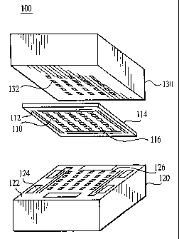
FIG. 2 shows an exploded view of the primary components of one illustrative
embodiment of an improved quasi-optical grid array system 100 according to the
present invention. The system includes a "substrate" 120, a "spatial power-
combining
semiconductor chip structure" (and more specifically, in this embodiment, a
quasi-
optical grid array) 110 and a "superstrate" 130. The~semiconductor chip
structure 110 .
has a grid array with active devices and patterned electrical conductors on
the front
surface 114 (not shown, but is similar to the patterns on the front surface of
the grid
array shown in FIG. 1) and patterned electrical conductors 116 on its back
surface
112. The chip may also include 'vial' connecting the conductors on its two
faces, or
surfaces, 114 and 116. The vias and the back surface conductors tend to
improve heat
removal from the array, and to improve flexibility in providing biasing and rf
matching for the grid array. Alternatively, the patterned conductors on the
back
surface of the chip may actually replace the patterned conductors that are
conventionally found on the front surface of grid arrays. In this variation,
the back
surface patterned metal would preferably be connected directly to the active
components on the front side of the array through vias. One advantage of
placing the
patterned conductors on the back surface is that the patterned metal does not
compete
for real estate on the back surface with components as it must on the front
surface of
the chip. Thus, it is possible to provide thicker metalization patterns on the
back
surface than is possible on the front side, thereby providing inherently lower
voltage
drops (lower resistance / higher efficiencies), simplified layout and enhanced
manufacturability.
The substrate 120 is. a slab made of any appropriate thermally-conductive
material, such as ceramic, and, in this embodiment, has patterned,
electrically-
conductive material (e.g. a metal pattern) 124, 126 disposed on its front
surface 122.
This material may also optionally be disposed on the back surface of the
substrate (not
shown). When mated with the patterned metal on back surface of the chip, this
patterned material can improve delivery of DC power to the active components
in the
array on the chip 110 (biasing)., can enhance the removal of waste heat from
the array,
and can improve radio frequency (rf) matching.
The superstrate 130 is a thermally conductive dielectric material such as a
ceramic slab or thermally conductive encapsulant. The superstrate may also
have
8
CA 02503826 2005-04-26
WO 2004/040357 PCT/US2003/034404
patterned electrically-conducting material 132 on its back surface in order to
enhance
heat removal from, and biasing and tuning for the grid array. Each section is
attached
to the adjacent section through a process andlor means that provides
mechanical
support, heat removal, and (in some embodiments) electrical connection.
Adjacent
sections may be attached, or joined, with thermally-conductive adhesives or
epoxies
and for regions in which there is metal-to-metal contact, any appropriate
bonding
technique and material, collectively called joint, may be used, such as
soldering,
thermo-compression, ultrasonic bonding, electrically-conductive adhesives or
any
appropriate combination of these techniques and/or materials.
Various permutations of these features that incorporate the principles of the
invention and result in novel spatial combining devices, such as quasi-optical
grid
array amplifiers or oscillators, with enhanced thermal properties and
potentially
improved biasing options are now described. One embodiment includes a spatial-
power combining chip 110 (with or without patterned metal on its back surface)
attached to the superstrate 130 and without a substrate 120. FIG. 3 shows in
cross-
sectional view, another alternative embodiment of an improved spatial power-
combining system 300 according to the present invention. In particular, the
system
includes two primary structures, namely, a quasi-optical grid array chip 310
and a
thermally-conductive, dielectric substrate 330. The chip has a front surface
312 and a
back surface 314 with patterned, electrically-conductive material 320 disposed
on the
back surface. The substrate also has patterned, electrically-conductive
material 340
disposed on it front surface 332. The chip is attached to the substrate by
joining the
two sets of patterned materials together via solder joint 350. DC bias is
supplied to
the devices on the chip's front surface 312 (not shown) either from the
patterns 320
on the back surface' by means of vias through the chip or by the conventional
means
of connecting the DC sources) to the patterns on the front surface 312.
FIG. 4 shows in cross-sectional view, a second alternative embodiment of an
improved spatial power-combining system 400 according to the present
invention. In
particular, the system includes three primary structures, namely, a quasi-
optical grid
array chip 410 and a substrate 430 and a superstrate 420. The back surface 414
of the
chip is attached to the front surface 432 of the substrate via a dielectric
thermally
conductive adhesive 450. The front surface 412 of the chip is attached to the
back
9
CA 02503826 2005-04-26
WO 2004/040357 PCT/US2003/034404
surface 422 of the superstrate via another dielectric thermally-conductive
adhesive
440.
FIG. 5 shows in cross-sectional view, a third alternative embodiment of an
improved spatial power-combining system 500 according to the present
invention. In
particular, the system includes three primary structures, namely, a quasi-
optical grid
array chip 510 and a substrate 530 and a superstrate 520. The chip has a front
surface
512 and a back surface 514 with patterned, electrically-conductive material
516
disposed on the back surface. The substrate also has patterned, electrically-
conductive material 534 disposed on its front surface 532. The chip is
attached to the
substrate by matching and joining the patterned materials 516 on the chip to
the
patterned material 534 on the substrate via solder joint 550. The back surface
522 of
the superstrate 520 is attached to the front surface 512 of the chip via a
dielectric
thermally-conductive adhesive 540.
DC bias is supplied to the devices on the chip's front surface 512 (not shown)
either from the patterns 516 on its back surface by means of vias through the
chip or
by the conventional means of connecting the DC sources) to the patterns on the
front
surface 512.
FIG. 6 shows in cross-sectional view, a fourth alternative embodiment of an
improved spatial power-combining system 600 according to the present
invention. In
particular, the system includes three primary structures, namely, a quasi-
optical grid
array chip 610 and a substrate 630 and a superstrate 620. The chip has a front
surface
612 and a back surface 614, each with patterned, electrically-conductive
material 616
and 61~ disposed thereon, respectively. The substrate also has patterned,
electrically-
conductive material 634 disposed on its front surface 632 that partly or
substantially
matches the metal pattern on the back surface 614 of the chip. The chip is
attached to
the substrate by joining the two sets of patterned materials 616, 634 together
via
solder joint 650. The back surface 622 of the superstrate 620 includes
patterned,
electrically-conductive material 624 disposed thereon. The chip is attached to
the
superstrate by matching and joining the patterned material 616 on the chip to
the
patterned material 624 on the superstrate via thermo-compression bonding at
640.
DC bias may be supplied via the conventional means to the front of the chip
itself, via
the metal patterns on the substrate, or via the metal pattern on the
superstrate, or via a
combination of the above.
CA 02503826 2005-04-26
WO 2004/040357 PCT/US2003/034404
Having thus described exemplary embodiments of the invention, it will be
apparent that further alterations, modifications, and improvements will also
occur to
those skilled in the art. Further, it will be apparent that the present
technique and
system is not limited for use with quasi-optical array structures (e.g. grid
amplifiers,
oscillators, mixers, etc.), but is applicable to any spatial power combiner
that can
benefit from being integrated with heat-removing and bias-supplying
structures.
Moreover, the present invention is not limited to spatial power combiners.
Rather, it
is applicable to any type of integrated semiconductor chip that cannot
properly
function with a conventional conducting solid ground plane that covers
substantially
the entire back surface of the chip, but can benefit from the selective
conducting
pattern structures and methods of the present invention. Accordingly, the
invention is
defined only by the following claims.
I1