Language selection

Search

Patent 2504050 Summary

Third-party information liability

Some of the information on this Web page has been provided by external sources. The Government of Canada is not responsible for the accuracy, reliability or currency of the information supplied by external sources. Users wishing to rely upon this information should consult directly with the source of the information. Content provided by external sources is not subject to official languages, privacy and accessibility requirements.

Claims and Abstract availability

Any discrepancies in the text and image of the Claims and Abstract are due to differing posting times. Text of the Claims and Abstract are posted:

  • At the time the application is open to public inspection;
  • At the time of issue of the patent (grant).
(12) Patent Application: (11) CA 2504050
(54) English Title: SMD CHIP HANDLING APPARATUS
(54) French Title: DISPOSITIF DE MANUTENTION DE PUCE CMS
Status: Deemed Abandoned and Beyond the Period of Reinstatement - Pending Response to Notice of Disregarded Communication
Bibliographic Data
Abstracts

English Abstract


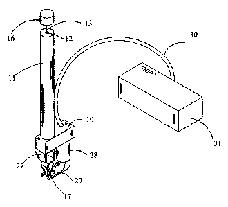
The apparatus is for securely fetching and positioning an SMD chip on a
printed circuit
board and soldering the same to the board. Two spring plates form the clasping
fingers which are
wedged apart to a width larger than the width of the SMD chip by an expander
formed on an
elongated rod slidably mounted within a vertical tubular housing. An SMD chip
may be safely
fetched by pressing the rod on the top of the SMD with a continuous depressing
motion until the
fingers clasp the SMD chip safely therebetween. A soldering unit with a
bifurcate soldering head
located juxtaposed to the fingers is operative to solder the SMD chip to the
printed circuit board
while the SMD chip is safely held in place.


Claims

Note: Claims are shown in the official language in which they were submitted.


The embodiments of the invention in which an exclusive property or privilege
is claimed
are defined as follows:
1. An apparatus for handling an SMD chip comprising:
a main body having a tubular housing extending vertically therefrom,
a vertical channel opening formed in said tubular housing and said main body,
an elongated rod slidably located within said channel opening, said rod having
a lower
portion extending below a lower edge of said main body,
an expander formed on said rod and located above a lower end of said rod,
two spring plates mounted to said main body and extending downwardly from said
main
body with lower end edges of said plates located juxtaposed to one another,
horizontally extending protruding sections formed in said plates, said
protruding sections
having inwardly pointing vertexes positioned opposite and in close proximity
to one another, said
vertexes being engageable with and wedged apart by said expender when said rod
slides upwards
relative to said tubular housing, said lower end edges of said spring plates
being spaced apart to a
widest space larger than a width dimension of said SMD chip when said expander
is located
between said vertexes, and a lower end of said rod is located below said lower
end edges of said
spring plates when said expander is located below said protruding sections.
2. An apparatus for handling an SMD chip according to Claim 1 wherein said rod
has an upper
portion extending above an upper end of said tubular housing, a button located
on said upper end
of said rod, and said lower end of said rod is located just above said lower
end edges of said
spring plates when said protruding sections are wedged by said expander to the
widest width.
3. An apparatus for handling an SMD chip according to Claim 2 wherein sand
expander has an
-9-

inverted conical shape.
4. An apparatus for handling an SMD chip according to Claim 2 wherein said
expander has a
spherical shape.
5. An apparatus for handling an SMD chip according to Claim 2 wherein said
expander has a
pear shape.
6. An apparatus for handling an SMD chip comprising:
a main body,
a tubular housing extending upwards vertically from said main body,
a elongated vertical through channel opening extending throughout said tubular
housing and
said main body,
an elongated rod extending slidably within said through channel opening, and
having an
upper end portion therein extending above a top end of said tubular housing
and a lower end
portion extending below a lower edge of said main body,
an expander formed on said lower end portion of said rod and located above a
lower end of
said rod,
two triangular shape spring plates mounted on said main body and extending
downwardly
below said lower edge of said main body in a convergent manner adjacent to
said through
channel opening with lower end edges of said spring plates normally in close
proximity to one
another,
horizontal inwardly protruding sections formed in said spring plates, said
protruding
sections having inwardly pointing vertexes normally located in close proximity
opposite to one
another, and said vertexes being engageable with and wedged apart by said
expander when said
-10-

rod moves upwards relative to said tubular housing to locate said expander at
a position between
said vertexes, said lower end edges of said spring plates being spaced apart
to a widest width
larger than a width of said SMD chip when said vertexes are wedged apart by
said expander, and
when said rod is in said position a lower end of said rod being located just
above said lower end
edges of said spring plates,
a soldering unit having a housing extending downward from said main body, said
soldering
unit having a bifurcate soldering head located juxtaposed to said lower end
edges of said spring
plates.
7. An apparatus according to Claim 6 including a press button mounted on an
upper end of
said rod, and said expander has an inverted conical shape.
8. An apparatus according to Claim 7 including a power supply connected to
said soldering
device by an electrical lead wire.
9. An apparatus according to Claim 8 wherein said spring plates are two
downwardly
extending plates of an inverted V-shaped spring clasp having an upper
horizontal flat section
mounted to an underside of said main body.
10. An apparatus for handling an SMD chip comprising:
a horizontal main body,
a tubular housing having a hollow interior and mounted vertically on said main
body,
a through channel opening extending vertically through said main body and in
communication with said hollow interior of said tubular housing,
an elongated rod extending slidably within said through opening of said main
body and
said hollow interior of said tubular housing, said rod being operative
slidably to locate a lower
-11-

end therein selectively between a lower position and an upper position,
a expander formed on a lower end portion of said rod and located above a lower
end of
said rod,
two spring plates mounted on said main body and extending downwardly below a
lower
surface of said main body adjacent to said through channel opening with lower
end edges of said
spring plates normally in close proximity to one another, said lower end of
said rod extending
outwards below said lower end edges of said spring plates when said rod is at
said lower
position, and said lower end of said rod being located just above said lower
end edges of said
spring plates when said rod at said upper position,
horizontal inwardly protruding sections formed in said spring plates, said
protruding
sections having inwardly pointing vertexes normally located in close proximity
opposite to one
another, said vertexes being engageable with and wedged apart by said expander
when said rod is
moved upwards relative to said tubular housing to locate said expander at a
position between said
vertexes, said lower end edges of said spring plates being spaced apart to a
widest width larger
than a width of said SMD chip when said vertexes are wedged apart by said
expander, and when
said expander is positioned below said protruding sections of said spring
plates when said rod is
at said lower position,
a latching mechanism incorporated in said tubular housing and operative for
retaining
said rod at said upper position.
11. A apparatus for handling an SMD chip according to Claim 10 wherein said
latching
mechanism includes a compression spring located at an upper end with said
hollow interior of
said tubular housing, a slider plate located between said compression spring
and an upper end of
-12-

said rod, a horizontal latching plate located within said tubular housing,
said latching plate
having a latching opening formed therein and an upper portion of said rod
extending through said
latching opening, said slider plate having a side arm extending horizontally
outward through a
side opening formed in said tubular housing, a push button mounted at an outer
end of said side
arm, a compression spring mounted around said side arm and located between
said push button
and said tubular housing, an annular retainer formed on said upper end portion
of said rod, said
annular retainer being engageable with an edge portion of said latch opening
to retain said rod at
said upper position.
12. An apparatus according to Claim 11 wherein said annular retainer has a
tapered upper
surface, and said latch opening has a downwardly sloping inner side wall
distal from said side
arm.
13. An apparatus according to Claim 12 including a soldering unit mounted to
said main body,
said soldering unit having a bifurcated soldering head extending juxtaposed to
said lower end
edges of said spring plates.
14. An apparatus according to Claim 13 wherein said protruding section of said
spring plates
are horizontal triangular sections having inwardly extending vertexes spaced
in close proximity
to one another.
15. An apparatus according to Claim 13 wherein said protruding section of said
spring plates
are arcuate sections having inwardly extending vertexes spaced in close
proximity to one another.
-13-

Description

Note: Descriptions are shown in the official language in which they were submitted.


CA 02504050 2005-04-11
SMD CHIP HANDLING APPARATUS
This invention relates to an apparatus for holding and soldering a miniature
size chip
component on a printed circuit board and more particularly relates to a
portable device for
facilitating electronic hobbyists and circuit developers in surface mounting
and soldering a
miniature SMD chip component on a printed circuit board or de-soldering it
therefrom.
Heretofore, it has been problematic for an electronic hobbyist and circuit
developer in
handling and soldering a surface mounted device, commonly referred to as an
SMD chip, on a
printed circuit board in fabricating a prototype electronic circuit.
Generally, an SMD chip has the
physical dimensions of 0.12 inch by 0.06 inch or 0.08 inch by 0.05 inch or
0.04 inch by 0.02
inch, and a height of about 0.025 inch. With such extremely small physical
dimensions, it is very
difficult and awkward to fetch and to place the SMD chip at a selected
position on the printed
circuit board, and maintaining it in position while soldering it onto the
board. A pair of tweezers
are commonly employed for manually picking up an SMD chip and placing it on
the printed
circuit board, and/or other means must be employed for retaining it in place
while soldering it to
the board otherwise the chip would be displaced from the desired position by
the melted solder.
Firstly, considerable care must be exercised in picking up an SMD chip with
the tweezers, as the
chip would fall off the tweezers if an insufficient clamping force is applied;
on the other hand,
the SMD chip would readily pop out from the tweezers if too much force is
applied.
Furthermore, the manual operation of maintaining the chip in place with the
tweezers or other
holding means during soldering, is also extremely difficult to carry out since
the tweezers or
holding means must be held in place, while having simultaneously to feed
solder with a solder
wire to the chip and to apply heat to the solder with a soldering iron. All
these different tasks may
-1-

CA 02504050 2005-04-11
not be carried out simultaneously by a single person.
Devices employing vacuum suction and/or pre-coated adhesive applied on the
printed
circuit board for resolving the above problems have been proposed. However,
such devices are
very complex in construction, and are still difficult to operate; and moreover
they are far too
S expensive to acquire by a hobbyist or an individual electronic circuit
developer for making
prototype electronic circuits.
It is therefore an object of the present invention to provide an apparatus for
fetching an
SMD chip effectively.
It is another object of the present invention to provide a portable apparatus
operative
manually for fetching and positioning an SMD chip on a printed circuit board
with ease.
It is another object of the present invention to provide an apparatus
operative for fetching,
positioning and retaining an SMD chip on a printed circuit board for soldering
purposes.
It is another object of the present invention to provide a portable manually
operative
apparatus for fetching, positioning, retaining and soldering an SMD chip on a
printed circuit
board.
It is yet another object of the present invention to provide a portable
manually operative
apparatus for retaining an SMD chip safely in place for de-soldering it from a
printed circuit
board and removing it therefrom.
It is still another object of the present invention to provide a manually
operative apparatus
which is simple in structure and easy to operate.
It is still another object of the present invention to provide a manually
operative portable
apparatus which is cost effective for hobbyists and an individual circuit
developers to acquire.
-2-

CA 02504050 2005-04-11
The description of the invention which follows, together with the accompanying
drawings
should not be construed as limiting the invention to the example shown and
described, because
those skilled in the art to which this invention appertains will be able to
devise other forms
thereof within the ambit of the appended claims. In the accompanying drawing
Figure 1 is a front perspective elevation view of the apparatus according to
the present
invention.
Figures 2, 3 and 4 are perspective side elevation view of the chip fetching
portion of the
apparatus showing the operation of fetching an SMD chip from a support
surface.
Figure S is an enlarged isolated perspective front view of the combination of
the SMD
chip fetching and retaining spring plates and soldering head of the present
apparatus.
Figure 6 is an isolated side elevation view of the spring plates and the rod
with an
expander having a pear shape.
Figure 7 is an isolated side elevation view of the spring plates and the rod
with an
expander having a spherical shape.
Figure 8 is an isolated side elevation view of the spring plates and the rod
with an
expander having an inverted triangular or conical shape.
Figures 9 through 11 are partial sectional side elevation views of the
alternative
embodiment of the apparatus of the present invention with a latching mechanism
for the rod
incorporated in the tubular housing.
With reference to the accompanying drawings wherein like reference numerals
designate
corresponding parts in the several views, the apparatus according to the
present invention has a
main body 10 which may be rectangular in shape as shown. An elongated tubular
housing 11
-3-

CA 02504050 2005-04-11
extends vertically upwards from a front portion of the main body 10. In the
exemplary
embodiment shown, the tubular housing 11 is preferably cylindrical in shape.
The tubular
housing 11 may be mounted to or integrally formed with the main body 10 by
molding. A
vertical through channel opening 12 is formed in the tubular housing 1 l and
the front portion of
the main body 10 directly below the tubular housing 11. An elongated rod 13 is
slidably mounted
within the channel opening 12. An upper portion 14 of the rod 13 extends above
the upper end of
the tubular housingl l and its lower end portion 15 extends beyond the lower
edge of the main
body 10. A button 16 is mounted on the upper end of the rod 13 such that the
rod 13 may be
operative freely vertically and slidably up or down the tubular housing 11 by
pressing or pulling
on the button 16. An expander 17 is formed at the lower end portion of the rod
13 and it is
located at a short distance from the lower end 18 of the rod 13. The expander
17 preferably has
an inverted conical shape as shown with its narrow end pointing upwards. It
may alternatively be
pear shape, spherical shape or triangular shape as shown in Figures 6, 7 and
8.
Two spring plates 19 and 20 extend downwardly adjacent the lower end of the
through
opening 12 from the main body 10 with their lower ends juxtaposed to one
another. The spring
plates 19 and 20 may be provided by two inverted triangular shape plates of a
generally inverted
V-shaped steel spring clasp having a joined upper flat section 21 mounted to
the underside of the
main body 10. The spring plates 19 and 20 may be rectangular or other similar
shape; however,
the inverted triangular shape as shown in the preferred embodiment provides a
more desirable
spring force and durability for the apparatus. The lower ends 22 and 23 of the
spring plates 19
and 20 respectively have a width similar to the length of an SMD chip. An
inwardly protruding
section is formed at the spring plates 19 and 20. The protruding section may
be provided by
-4-

CA 02504050 2005-04-11
horizontal triangular sections 24 and 25 formed in the spring plates 19 and 20
respectively as
shown with the vertexes 26 and 27 of the triangular sections 24 and 25
pointing inwards to touch
or to space in close proximity to one another. Alternatively, the protruding
section may be an
arcuate section as shown in Figure 8. The vertexes 26 and 27 will be wedged
apart by the
expander 17 when the rod 13 slides upwards relative to the spring plates 19
and 20 to locate
between these vertexes 26 and 27 so as to force the lower edges 22 and 23 of
the spring plates 19
and 20 to space apart from one another to a widest width larger than the width
of an SMD chip.
The expander 17 is located at a position above the lower end of the rod 13
such that when the
triangular sections 24 and 25 are wedged apart to the widest width by the
expander 17, the lower
end 18 of the rod 13 will be located slightly above the lower edges 22 and 23
of the spring plates
19 and 20. Normally, when the expander 17 is located below the triangular
sections 24 and 25,
the lower end of the rod 13 extends outwards below the lower edges 22 and 23.
A soldering unit 28 is mounted to the main body 10 and extending downwardly
therefrom. The housing of the soldering unit 28 may also be integrally formed
on the main body
10 by molding. The soldering unit 28 has a bifurcate soldering head 29
extending sideway to
locate in close proximity juxtaposed to the lower edges 22 and 23 of the
spring plates 19 and 20.
An electrical lead 30 conducts the electrical power required for operating the
soldering unit 28.
The electrical power may be provided by a battery 31 or a step-down
transformer connected to
the household AC supply.
As best shown in Figures 2, 3 and 4, an SMD chip 32 lying on a support surface
may be
fetched by vertically pressing the lower end of the rod 13 on the top of the
SMD chip 32 with a
continuous depressing motion. The action will first retain the SMD temporarily
and securely in
-5-

CA 02504050 2005-04-11
place on the support surface by the rod 13. The continuous pressing motion
will cause the rod 13
to move effectively upwards relative to the spring plates 19 and 20 until the
triangular sections
24 and 25 are wedged apart by the expander 17. At this same moment, the lower
edges 22 and 23
will be spaced apart to the widest width larger than the width of the SMD chip
32 to allow the
lower edges 22 and 23 to move downwards to locate adjacent to the sides of the
SMD chip.
When the lower edges 22 and 23 reach the supporting surface, the expander 17
will have slid
upwards past the vertexes 26 and 27 and the lower edges 22 and 23 of the
spring plates 19 and 20
will snap close to clasp the SMD firmly. The entire operation can be carried
out in a continuous
motion with the SMD chip 32 constantly held firmly in place on the support
surface at all time by
the lower end of the rod 13. The spring plates 19 and 20 are designed so that
their lower ends will
provide the desirable su~cient spring force for holding the SMD chip 32
securely therebetween.
The SMD chip 32 may then be carried safely by the apparatus to position onto
the selected
location on the printed circuit board 33, and it then may be positioned firmly
on the printed
circuit board 33 by pressing down on the apparatus so that it is restrained in
place by the spring
plates 19 and 20 as well as being pressed downwards firmly by the rod 13. With
the SMD chip
32 now safely placed on the printed circuit board 33, the soldering unit 28 is
operated while
feeding a fluxed solder wire 34 to the soldering head 29 for soldering the SMD
chip 32 onto the
printed circuit board 33. Because of the close proximity of the soldering head
29 to the SMD
chip 32, the soldering operation may be executed expeditiously. The flux
inside the solder wire
34 will evaporate within a short period of time which reduces the flux
cleaning reaction.
The present apparatus may also be used for de-soldering an SMD chip from the
printed
circuit board, which may be carried out by positioning the apparatus onto the
SMD chip to be
-6-

CA 02504050 2005-04-11
removed for holding the SMD chip in place while the soldering unit 28 is
operated to melt the
solder therefrom. The melted solder is removed with a suction pump in the
conventional manner
while the SMD chip is securely held in place. The de-soldered SMD chip may
then be removed
effectively from the printed circuit board with the SMD chip securely held
between the spring
plates 19 and 20.
An alternative embodiment of the present apparatus is shown in Figures 9
through 11. A
spring biassed latch mechanism 32 is incorporated in the tubular housing 1 l,
which normally
maintains the rod 13 in the position with its lower end extending outwards
below the lower edges
of the spring plates 19 and 20. The tubular housing 11 may have a closed upper
end and it may be
removably mounted to the main body 10 to facilitate repair or replacement of
parts in the latch
mechanism 32. A compression spring 33 is located within the top end of the
tubular housing 11.
A slider plate 34 is located between the top end of the rod 13 and the
compression spring 33. The
slider plate 34 may be alternatively integrally formed on the top end of the
rod 13. A latch plate
35 is located in the tubular housing 11 in a horizontal manner and it has a
side arm 36 extending
horizontally outward slidably through a side opening 37 formed in the tubular
housing 11. A
push button 38 is mounted at the outer end of the side arm 36, and a
compression spring 39 is
mounted on the side arm 36 and located between the tubular housing 11 and the
push button 38.
The compression spring 39 normally urges the side arm 36 to extend outwards.
'The latch plate 35
may be moved sideways horizontally by pushing the push button 38 to press the
side arm 36
inwards against the spring force of the compression spring 39. A latch opening
40 is formed in
the latch plate 35. T'he upper end portion of the rod 13 extends through the
latch opening 40. The
latch opening 40 preferably has a downwardly sloping inner side wall 41 distal
from the side arm
_7_

CA 02504050 2005-04-11
36. An annular retainer 42 is mounted on the rod 13. The annular retainer 42
has a diameter
larger than the diameter of the rod but smaller than the diameter of the latch
opening 40 and it
has a relatively flat horizontal lower surface 43 and a tapered upper surface
44. The annular
retainer 42 is mounted at a position on the rod 13 at which when the expander
17 just passes the
vertexes 26 and 27 of the spring plates 19 and 20 by pressing the rod 13 on
the SMD chip against
the spring force of the compression spring 33, the annular retainer 42 will
have moved just above
the latch opening 40. Since the latch plate 35 is biassed by the compression
spring 39, the lower
surface 43 of the annular retainer 42 will engage with the upper edge of the
latch opening 40 as
soon as the annular retainer 42 passes the latch opening 40 to retain the rod
13 at this pushed up
position with the SMD chip 32 already clasped firmly by the lower edges 22 and
23 of the spring
plates 19 and 20. The rod 13 may be returned to the lower position by pressing
the push button
38 inwards against the spring force of the compression spring 39 to disengage
the annular
retainer 42 from the latch opening 40 such that the spring force of the
compression spring 33 will
push the rod 13 to return to the lower position with its lower end extending
outwards below the
lower edges 22 and 23 of the spring plates 19 and 20. The tapered upper
surface 44 of the annular
retainer 42 and the downwardly sloping inner side wall 41 of the latch opening
40 facilitate the
sliding movement of the annular retainer 42 through the latch opening 40
during the latching
operation.
Thus the several aforementioned objects and advantages are most effectively
attained.
Although the preferred embodiments of the invention have been disclosed and
described in detail
herein, it should be understood that this invention is in no sense limited
thereby and its scope is
to be determined by that of the appended claims.
_g_

Representative Drawing
A single figure which represents the drawing illustrating the invention.
Administrative Status

2024-08-01:As part of the Next Generation Patents (NGP) transition, the Canadian Patents Database (CPD) now contains a more detailed Event History, which replicates the Event Log of our new back-office solution.

Please note that "Inactive:" events refers to events no longer in use in our new back-office solution.

For a clearer understanding of the status of the application/patent presented on this page, the site Disclaimer , as well as the definitions for Patent , Event History , Maintenance Fee  and Payment History  should be consulted.

Event History

Description Date
Revocation of Agent Requirements Determined Compliant 2021-04-01
Application Not Reinstated by Deadline 2010-04-12
Time Limit for Reversal Expired 2010-04-12
Deemed Abandoned - Failure to Respond to Maintenance Fee Notice 2009-04-14
Application Published (Open to Public Inspection) 2006-10-11
Inactive: Cover page published 2006-10-10
Inactive: First IPC assigned 2005-06-21
Filing Requirements Determined Compliant 2005-05-16
Inactive: Filing certificate - No RFE (English) 2005-05-16
Application Received - Regular National 2005-05-16
Small Entity Declaration Determined Compliant 2005-04-11

Abandonment History

Abandonment Date Reason Reinstatement Date
2009-04-14

Maintenance Fee

The last payment was received on 2008-03-27

Note : If the full payment has not been received on or before the date indicated, a further fee may be required which may be one of the following

  • the reinstatement fee;
  • the late payment fee; or
  • additional fee to reverse deemed expiry.

Please refer to the CIPO Patent Fees web page to see all current fee amounts.

Fee History

Fee Type Anniversary Year Due Date Paid Date
Application fee - small 2005-04-11
MF (application, 2nd anniv.) - small 02 2007-04-11 2007-02-05
MF (application, 3rd anniv.) - small 03 2008-04-11 2008-03-27
Owners on Record

Note: Records showing the ownership history in alphabetical order.

Current Owners on Record
CHI MING WONG
WOON-WAI CHAN
Past Owners on Record
None
Past Owners that do not appear in the "Owners on Record" listing will appear in other documentation within the application.
Documents

To view selected files, please enter reCAPTCHA code :


To view images, click a link in the Document Description column. To download the documents, select one or more checkboxes in the first column and then click the "Download Selected in PDF format (Zip Archive)" or the "Download Selected as Single PDF" button.

List of published and non-published patent-specific documents on the CPD .

If you have any difficulty accessing content, you can call the Client Service Centre at 1-866-997-1936 or send them an e-mail at CIPO Client Service Centre.


Document
Description 
Date
(yyyy-mm-dd) 
Number of pages   Size of Image (KB) 
Abstract 2005-04-11 1 22
Description 2005-04-11 8 399
Claims 2005-04-11 5 217
Drawings 2005-04-11 5 71
Representative drawing 2006-09-21 1 7
Cover Page 2006-10-02 1 36
Filing Certificate (English) 2005-05-16 1 157
Reminder of maintenance fee due 2006-12-12 1 112
Courtesy - Abandonment Letter (Maintenance Fee) 2009-06-09 1 172
Reminder - Request for Examination 2009-12-14 1 117
Fees 2007-02-05 2 43