Note: Descriptions are shown in the official language in which they were submitted.
CA 02504128 2005-04-27
WO 2004/049048 PCT/US2003/037267
-1-
EMBEDDED ELECTRODE INTEGRATED OPTICAL DEVICES
AND METHODS OF FABRICATION
The present invention relates to optical signal transmission and, more
specifically,
to improved waveguide devices useful in applications requiring modulation,
attenuation,
polarization control, and switching of optical signals.
Integrated optical devices including embedded electrodes and methods of
fabrication of such devices are provided. In accordance with one embodiment of
the
present invention, a method of fabricating an integrated optical device is
provided. The
method comprises the acts of: (i) providing a support wafer defining an
electrode support
surface; (ii) forming an electrode pattern over the electrode support sunace
of the
support wafer; (iii) forming a non-polymeric buffer layer on at least a
portion of the
electrode pattern and over at least a portion of the support wafer; (iv)
forming a waveguide
core material layer over the non-polymeric silica-based buffer layer; (v)
removing portions
of the core material layer to define a waveguide core; and (vi) positioning a
cladding
material in optical communication with the waveguide core such that the buffer
layer, the
cladding material, and the waveguide core define an optically-clad waveguide
core.
In accordance with another embodiment of the present invention, the buffer
layer is
formed over the electrode pattern and the support wafer through a sol-gel
process
characterized by a maximum processing temperature below about 400°C.
In accordance with yet another embodiment of the present invention, an
integrated
optical device is provided comprising a support wafer, an electrode pattern, a
non-
polymeric silica-based buffer layer, a waveguide core material layer, and a
cladding
material. The support wafer defines an electrode support surface. The
electrode pattern is
formed over the electrode support surface of the support wafer. The non-
polymeric silica-
based buffer layer is formed on at least a portion of the electrode pattern
and over at least a
portion of the support wafer. The waveguide core material layer is formed over
the buffer
layer. The cladding material is in optical communication with the waveguide
core such
that the buffer layer, the cladding material, and the waveguide core define an
optically-
clad waveguide core.
CA 02504128 2005-04-27
WO 2004/049048 PCT/US2003/037267
-2_
Accordingly, it is an object of the present invention to provide improved
waveguide devices and a scheme for fabricating improved waveguide devices
useful in
applications requiring modulation, attenuation, polarization control, and
switching of
optical signals. Other objects of the present invention will be apparent in
light of the
description of the invention embodied herein.
The following detailed description of specific embodiments of the present
invention can be best understood when read in conjunction with the following
drawings,
where like structure is indicated with like reference numerals and in which:
Figs. 1-3 are schematic illustrations, taken in cross section, of embedded
electrode
integrated optical devices according to various embodiments of the present
invention.
Fig. 4 is a schematic illustration, take in plan view, of portions of the
integrated
optical devices illustrated in Figs. 1-3.
Figs. 5-7 illustrate a method of fabricating integrated optical devices
according to
the present invention;
Figs. ~-12 are schematic illustrations, taken in cross section, of integrated
optical
devices according to various embodiments of the present invention including
control
electrodes in addition to the embedded electrodes illustrated in Figs 1-3;
Fig. 13 is an illustration of an alternative embedded electrode design
according to
the present invention; and
Figs. 14 and 15 are schematic illustrations, taken in cross section, of
further
integrated optical devices according to various embodiments of the present
invention.
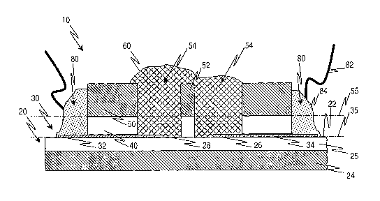
Referring initially to Figs. 1-4, integrated optical devices 10 according to
the
present invention are illustrated. It is noted that the devices 10 are
illustrated in a
somewhat generic nature because the devices 10 may take the form of any one of
a variety
of specific types of waveguide devices where embedded electrodes, an optically
functional
or non-functional cladding, and an optically functional or non-functional
waveguide core
are employed. For example, the teachings of the present invention may be
employed in
the context of one or more devices disclosed in published U.S. Patent
Applications
2003/0174982-A1 (Electrode and Core Arrangements for Polarization Independent
Waveguides) and 20031005919-Al (Waveguides and Devices Incorporating Optically
Functional Cladding Regions). The teachings of the present application may be
utilized
CA 02504128 2005-04-27
WO 2004/049048 PCT/US2003/037267
-3-
with the teachings of these and other pertinent references to render any one
of variety of
workable devices and fabrication schemes.
Referring again to Figs. 1-4, each integrated optical device 10 comprises a
support
wafer 20, an electrode pattern 30, a non-polymeric silica based buffer layer
40, a
waveguide material layer 50 and core 52, a cladding material 60, and one or
more contact
regions 80. The support wafer 20 is provided as a silicon wafer 24 carrying a
silica
coating 25, the silica coating defining an electrode support surface 22. The
electrode
pattern 30 is formed over the electrode support surface 22 of the support
wafer 20. The
buffer layer 40 is formed over the electrode pattern 30 and the support wafer
20. The
waveguide core material layer 50 is formed over the buffer layer 40.
For the purposes of describing and defining the present invention, it is noted
that a
distinction is intended between the respective meanings of the positional
terms "over" and
"on." Specifically, if a layer is formed "over" another layer it is
contemplated that an
intervening layer of another material may be present between the two layers.
In contrast,
if a layer is formed "on" another layer, no intervening layer is contemplated.
For example,
referring to Fig. 1, the core material layer 50 may be said to be formed
"over," but not
"on" the support wafer 20.
As will be described in further detail herein, the electrode pattern 30, the
buffer
layer 40, and the waveguide core 52 are formed such that the electrode pattern
30, which
may include one or more electrically isolated, substantially co-planar control
electrodes
32, 34, is embedded in the device beneath the waveguide core 52. One or more
contact
regions 80 are formed over the electrode pattern 30. Conductive leads 82 may
be brought
into contact with the electrode pattern 30 in the contact regions 80 with the
aid of a
conductive epoxy 84, via wire bonding, or through any other suitable means for
conductively coupling the leads 82 to the electrode pattern 30. Prior to
bringing the
conductive leads 82 into contact with the electrode pattern, the pair of
contact regions may
be treated with hydrofluoric acid or another suitable material to remove
residual insulating
material, including residual cladding material, from the pair of contact
regions 80.
The various fabrication methods according to the present invention may be
described with reference Figs. 5-7. Initially, the support wafer 20 defining
the electrode
support surface 22 is provided. The electrode pattern 30 is formed over the
electrode
CA 02504128 2005-04-27
WO 2004/049048 PCT/US2003/037267
-4-
support surface 22 of the support wafer 20 (see Fig. 5). Next, the non-
polymeric, silica
based buffer layer 40 is formed over the electrode pattern 30 and the support
wafer 20. A
waveguide core material layer 50 is formed over the buffer layer 40 (see Fig.
6). Portions
of the core material layer 50 are removed to define a waveguide core 52 and a
pair of
cladding containment regions 54 extending along opposite sides of the
waveguide core 52
in a direction substantially parallel to a longitudinal dimension of the
waveguide core 52
(see Fig. 7). In this manner, the cladding material 60 illustrated in Figs. 1-
3, which is
often initially a substantially non-rigid material like a gel or a viscous
fluid, may be
positioned within the pair of cladding containment regions 54, in optical
communication
with the waveguide core 52. The cladding containment regions provide an
effective
means by which the cladding material 60 may be presented in the device 10 in a
stable
manner.
As is illustrated in Figs. 1-3, the extent to which buffer layer removal is
effected
during formation of the cladding containment regions 54 may vary. For example,
in the
embodiment of Fig. 1, substantially all of those portions of the buffer layer
40 aligned with
the cladding containment regions 54 are removed during formation of the
cladding
containment region. In contrast, referring to the embodiment of Fig. 2, the
buffer layer 40
is Ieft largely unaffected by the cladding containment region forming step. In
Fig. 3,
substantial portions of the buffer layer 40 aligned with the cladding
containment regions
54 remain, defining a remaining protective layer 42 over the electrode pattern
within the
cladding containment regions 54.
In the embodiments of Figs. 2 and 3, the remaining buffer layer thickness in
the
cladding containment regions 54 is sufficient to form an electrically
insulative barrier
between the pair of control electrodes 32, 34. As is illustrated in Fig. 7, if
substantially all
of the buffer layer thickness in the cladding containment regions 54 is
removed, it may be
preferable to provide an electrically insulative barrier layer 70 over the
pair of control
electrodes 32, 34 prior to positioning the cladding material within the pair
of cladding
containment regions 54. The insulative barrier layer 70 may comprise silica or
any other
suitable electrical insulating material.
The above description of the fabrication steps according to the present
invention is
general in nature because it is contemplated that a variety of suitable
fabrication steps may
CA 02504128 2005-04-27
WO 2004/049048 PCT/US2003/037267
-5-
be employed within the scope of the present invention. For example, referring
to Fig. 1,
by way of illustration and not limitation, it is contemplated that the
waveguide core 52
may be formed through a process by which the position of the core 52 in a
plane 55 offset
from and generally parallel to a plane 35 occupied by the control electrodes
32, 34 is
controlled relative to respective positions of the pair of control electrodes
32, 34 in the
control electrode plane 35. For example, by way of illustration and not
limitation,
appropriate portions of the core layer 50 may be removed by patterning the
core material
layer utilizing a waveguide mask and, e.g., reactive ion etching the waveguide
structure.
The electrode pattern 30 may comprise any suitable conductive material. It is
contemplated, for example, that Au, Pt, Cr, Ta, Ti, indium tin oxide, and
combinations
thereof, may be suitable conductive materials. Cr is likely to be advantageous
in many
embodiments because of its good adhesive characteristics and relatively low
resistivity.
Particularly advantageous conductive materials will be characterized by
melting points of
at least about 1500°C. Referring to Fig. 13, it is contemplated that
the electrode pattern
may comprise first and second conductive layers 36, 38 - the first conductive
layer 36
having relatively enhanced adhesive properties and the second conductive layer
38 having
relatively enhanced conductive properties. The electrode pattern may define a
thickness of
between about 600 A and about 20,000 ~.
The buffer layer 40 and cladding material 60 preferably comprise materials
having
refractive indices that are lower than the refractive index of the core
material 50 at an
operating temperature and operating wavelength of the device. For example,
where the
core 52 comprises a material characterized by a refractive index of between
about 1.450
and about 1.455 at a selected operating temperature and operating wavelength
of the
device, the buffer layer 40 and the cladding material 60 may comprise
materials
characterized by refractive indices of between about 1.440 and about 1.450.
The buffer
layer 40 and the cladding material 60 are preferably transmissive to light of
at least one
commonly used telecommunication wavelength, e.g, about 860nm, about 1.3~,m,
and
about 1.55~m, or at a selected operational wavelength of the device 10.
It may be advantageous to ensure that the buffer layer 40 comprises an
electrically
insulating, non-metallic material. For example, the buffer layer may comprise
a material
selected from silica, SiOx (1.5<x<2), SiON, an insulating metal-oxide glass,
and
CA 02504128 2005-04-27
WO 2004/049048 PCT/US2003/037267
-6-
combinations thereof. Typical buffer layer dimensions range from between about
3~,m
and about 101Zm in thickness, although it is contemplated that a variety of
thickness
dimensions will be suitable.
According to one embodiment of the present invention, the buffer layer 40 is
formed through a sol-gel process characterized by a maximum processing
temperature
below about 400°C. In this manner, the buffer layer 40 can be formed at
processing
temperatures that are not likely to result in damage to or degradation of the
electrode
pattern 30. Sol-gel processing may be utilized to form passive, active, and
nonlinear
optical materials for optical devices according to the present invention. Many
of the
principles and desirable features of photolithographic definition can be
extended to sol-gel
materials. Sol-gel techniques, in which glasses are formed from organic
precursors by low
temperature polymerization reactions, offer attractive advantages in terms of
flexibility of
composition and structure. Generally, sol-gel processes consist of three
steps: first, a
colloidal suspension of oxide particles (the "sol") is formed by hydrolysis
and
condensation of a precursor (e.g. and alkoxide); next, the sol is dried such
that further
condensation creates a semi-rigid "gel"; finally, heat treatment of the gel is
used to
eliminate remaining organic ligands and to complete densification. The sol may
be dip,
spin, or spray-coated. Thick films can be obtained by multiple coatings.
It is contemplated that other processing schemes may be employed to form the
buffer layer 40. In the event the buffer layer 40 comprises a high melting
point silica-
based material 21 (mp>1500°C), preferred processing schemes should be
selected where
buffer layer formation may be achieved at temperatures well below (e.g., at
least about
500°C below) the melting point of the silica-based material 40 and the
melting point of
significant or major constituents of the electrode pattern 30. In this manner,
buffer layers
according to the present invention may be formed without causing undue damage
to the
materials of the electrode pattern 30. For example, in addition to the sol-gel
processed
described above, the buffer layer 40 may be formed through a plasma enhanced
chemical
vapor deposition process characterized by a maximum processing temperature
below, e.g.,
about1000°C.
The waveguide core material layer 50 may comprise any material suitable for
operation as a waveguide core. For example, suitable materials include, but
are not
CA 02504128 2005-04-27
WO 2004/049048 PCT/US2003/037267
_'7_
limited to, polymers, silica, doped silica, and combinations thereof. The
waveguide core
material layer 50 may be formed over the buffer layer 40 through a sol-gel
process in a
manner similar to that described above with reference to the buffer layer 40.
The core
layer 50 preferably comprises a material that is transmissive to light at
g60nm, 1.3~.m,
1.55~m, or any suitable telecommunication or operational wavelength of the
device 10.
Although a variety of core layer dimensions are contemplated by the present
invention,
typical core layers define a thickness of between about 3~m and about 10~m.
The cladding material 60 may comprise an electrooptic medium or any other
medium where a control signal applied to the electrode pattern 30 alters the
velocity,
phase, polarization, amplitude, or some other transmission characteristic of
light
propagating along the waveguide core 52. Although a variety of conventional
cladding
mediums are suitable for use in the present invention, it is noted that the
above-noted
patent documents include further teachings relative to selection of a suitable
medium. For
example, the cladding medium may comprise a polymeric or non-polymeric medium.
Examples of polymeric cladding mediums include, but are not limited to,
thermoplastics,
thermosets, UV cured materials, cross linked materials, and sol-gel materials.
The
cladding material 60 may include an electrooptic chromophore and may comprise
a
Pockels effect medium, a Kerr effect medium, or combinations thereof. As is
described in
further detail below with reference to Figs. 14 and 15, the core material
forming the
waveguide core 52 may also comprise a medium where a control signal applied to
the
electrode pattern 30 alters the velocity, phase, polarization, amplitude, or
other
transmission characteristic of light propagating along the waveguide core 52.
The cladding material 60 may be positioned within the cladding containment
regions through a sol-gel process in a manner similar to that described above
with
reference to the buffer layer 40. The cladding material 60 may also be
positioned within
the cladding containment regions 54 as a solution, as an aerosol of a
solution, as a vapor
deposited material, or as an electro-deposited material. As is illustrated in
Figs. 1-3, the
cladding material 60 may define a thickness at least as large as a thickness
defined by the
core material layer 50.
Where a poled cladding material 60 is preferred, the cladding material 60 may
be
positioned within the cladding containment regions 54 while a poling voltage
is applied
CA 02504128 2005-04-27
WO 2004/049048 PCT/US2003/037267
_g_
across the electrode pattern 30. Preferably, the poling voltage is maintained
during curing,
cross-linking, drying, or thermo-setting of the cladding material. For
example, where the
cladding material 60 comprises an electrooptic chromophore, a poling voltage
is applied
so as to be sufficient to orient the chromophore along the poling field in the
cladding
material 60. As is illustrated in Fig. 7, the electrically insulative barrier
layer 70 may be
formed over the electrode pattern prior to application of the poling voltage
and positioning
of the cladding material 60 over the electrically insulating layer 70.
Referring now to Figs. 8-11, it is noted that an additional electrode pattern
90 may
be formed on an electrode superstrate 92 of silica or other suitable material
and positioned
above the electrode pattern 30 formed over the electrode support surface 22 of
the support
wafer 20. In Fig. 8, for example the additional electrode pattern 90 comprises
a single
control electrode substantially aligned with the waveguide core ~2. In Fig. 9,
the
' additional electrode pattern 90 comprises a single control electrode offset
along one side
of the waveguide core 52 while the electrode pattern 30 formed over the
electrode support
surface 22 of the support wafer 20 comprises a single control electrode offset
along an
opposite side of the waveguide core 52. The contour of the resulting electric
field is
predominantly horizontal in areas relatively close to the core 52 and
predominantly
vertical in portions of the cladding material offset from the core 52. In this
manner, the
contour of the electric field is such that the respective orientations of the
electric field and
the poling contour are configured to compensate for optical birefringence of
the poled
cladding material or optically functional core material. As a result, the TM
mode index of
the waveguide device 10 can be substantially equal to the TE mode index of the
waveguide device 10. Alternatively, the electrodes and core may be configured
such that
changes in the respective indices are substantially equal. In addition, it is
contemplated
that the electrodes and core may be configured to affect only one of the
polarization
modes.
The electrode configuration of the embodiment of Figs. 10-12 are also directed
at
ensuring that the TM mode index of the waveguide device 10 can be
substantially equal to
the TE mode index of the waveguide device 10. Specifically, in Fig. 10, a
single control
electrode of the additional electrode pattern 90 is offset along one side of
the waveguide
core 52 and defines a thickness sufficient to extend alongside a substantial
portion of the
CA 02504128 2005-04-27
WO 2004/049048 PCT/US2003/037267
-9-
waveguide core 52. The control electrode of the electrode pattern 30 is offset
along the
opposite side of the waveguide core 52. The resulting contoured electric field
is
predominantly horizontal on the side of the core 52 with the enhanced
thickness electrode
and predominantly vertical on the opposite side of the core 52.
Similarly, in Fig. 11, one of the control electrodes of the additional
electrode
pattern 90 is offset along one side of the waveguide core 52 and defines a
thickness
sufficient to extend alongside a substantial portion of the waveguide core 52.
An
additional control electrode of the electrode pattern 90 is offset along the
opposite side of
the waveguide core 52 and defines a reduced thickness. The resulting contoured
electric
field is predominantly horizontal on the side of the core 52 with the enhanced
thickness
electrode and predominantly vertical on the opposite side of the core 52.
In Fig. 12, the additional electrode pattern 90 comprises a pair of control
electrodes
offset along opposite sides of the waveguide core 52. The electrode pattern 30
formed
over the electrode support surface 22 of the support wafer 20 comprises a
single control
electrode substantially aligned with the waveguide core 52. The resulting
contoured
electric field is predominantly vertical in the areas of the cladding 60
aligned with the pair
of control electrodes of the additional electrode pattern 90, predominantly
horizontal in the
areas of the cladding adjacent to the core, and predominantly vertical in the
area of the
core 52.
Referring to Figs. 14 and 15, the material forming the core 52 may comprise an
optically functional material, i.e., an electrooptic medium or any other
medium where a
control signal applied to the electrode patterns 30, 90 alters the velocity,
phase,
polarization, amplitude, or some other transmission characteristic of light
propagating
along the waveguide core 52. In the embodiments of Figs. 14 and 15, portions
of the
buffer layer 40 are removed to define a core material containment region in
which the core
material is introduced. The core material containment region is defined in the
buffer layer
40 prior to formation of the waveguide core 52 over the buffer layer. For the
purposes of
defining and describing the present invention, it is noted that the core 52 is
described as
being formed "over" the buffer layer 40, even though it is not positioned
above the entire
buffer layer 40.
CA 02504128 2005-04-27
WO 2004/049048 PCT/US2003/037267
-10-
In the embodiment of Fig. 14, the waveguide core material extends beyond the
core material containment region to define a core material overlayer 56. In
contrast, in the
embodiment of Fig. 15, the waveguide core material is substantially confined
within the
core material containment region defined by the buffer layer 40.
Figs. 14 and 15 also illustrate two different types of electrode arrangements.
It is
contemplated that any of a variety of suitable electrode arrangements may be
employed in
the embodiments of Figs. 14 and 15, including those illustrated in the
remaining
embodiments of the present application.
For the purposes of defining and describing the present invention, it is noted
that
the wavelength of "light" or an "optical signal" is not limited to any
particular wavelength
or portion of the electromagnetic spectrum. Rather, "light" and "optical
signals," which
terms are used interchangeably throughout the present specification and are
not intended
to cover distinct sets of subject matter, are defined herein to cover any
wavelength of
electromagnetic radiation capable of propagating in an optical waveguide. For
example,
light or optical signals in the visible and infrared portions of the
electromagnetic spectrum
are both capable of propagating in an optical waveguide. An optical waveguide
may
comprise any suitable signal propagating structure. Examples of optical
waveguides
include, but are not limited to, optical fibers, slab waveguides, and thin-
films used, for
example, in integrated optical circuits.
For the purposes of describing and defining the present invention it is noted
that
the term "substantially" is utilized herein to represent the inherent degree
of uncertainty
that may be attributed to any quantitative comparison, value, measurement, or
other
representation. The term "substantially" is also utilized herein to represent
the degree by
which a quantitative representation may vary from a stated reference without
resulting in a
change in the basic function of the subject matter at issue.
Having described the invention in detail and by reference to specific
embodiments
thereof, it will be apparent that modifications and variations are possible
without departing
from the scope of the invention defined in the appended claims. For example,
with
reference to the various embodiments of the present invention, it is noted
that the various
core, cladding, buffer, and overlayer regions of the present invention, and
different
respective portions thereof, may comprise optically functional or non-
functonal materials.
CA 02504128 2005-04-27
WO 2004/049048 PCT/US2003/037267
-11-
It is also noted that waveguide devices according to the present invention may
be
employed in a telecommunications or other type of optical network. In
addition, although
some aspects of the present invention are identified herein as preferred,
typical, or
particularly advantageous, it is contemplated that the present invention is
not necessarily
limited to these aspects of the invention.