Note: Descriptions are shown in the official language in which they were submitted.
CA 02504343 1994-10-26
'~ 50338-9E
1
METHOD FOR ELECTRONIC ASSEMBLY OF NANOPARTICLES
This is a divisional application of Canadian Patent
Application No. 2,175,483 filed October 26, 1994.
Field of the Invention
This invention pertains to the design,
fabrication, and uses of a self-addressable, self-assembling
microelectronic system which can actively carry out and
control multi-step and multiplex reactions in microscopic
formats. In particular, these reactions include molecular
biological reactions, such as nucleic acid hybridizations,
antibody/antigen reactions, clinical diagnostics, and
biopolymer synthesis.
The invention encompasses several aspects,
including devices and methods. Only the devices are claimed
in the parent application and only the methods are claimed in
this divisional application. However, it should be
understood that the expression "the present invention" also
covers those other aspects not claimed in this divisional
application.
More specifically, the method claimed in this
divisional application is for synthesizing structures
utilizing electronic transport of constituent components on
a device including at least a first microlocation,
comprising the steps of: attaching a first component to the
first microlocation, and subsequently electronically
transporting a second component to the first microlocation,
the second component comprising a functionalized
Tnanoparticle, whereby the first component interacts with the
second component as specific binding entities.
CA 02504343 1994-10-26
' ' 50338-9E
1a
Background of the Invention
Molecular biology comprises a wide variety of
techniques for the analysis of nucleic acid and protein, many
of which form the basis of clinical diagnostic assays. These
techniques include nucleic acid hybridization analysis,
restriction enzyme analysis, genetic sequence analysis, and
separation and purification of nucleic acids and proteins
(See, e.g., J. Sambrook, E. F. Fritsch, and T. Maniatis,
Molecular Cloning: A Laboratory Manual, 2 Ed., Cold Spring
Harbor Laboratory Press, Cold Spring Harbor, New York, 1989).
Most molecular biology techniques involve carrying
out numerous operations (e. g., pipetting) on a large number
of samples. They are often complex and time consuming, and
generally require a high degree of accuracy. Many
techniques are limited in their application by a lack of
sensitivity, specificity, or reproducibility. For example,
problems with sensitivity and specificity have so far
limited the application of nucleic acid hybridization.
CA 02504343 1994-10-26
2
Nucleic acid hybridization analysis generally
involves the detection of a very small numbers of specific
target nucleic acids (DNA or RNA) with probes among a
large amount of non-target nucleic acids. In order to
keep high specificity, hxbridization is normally carried
out under the most stringent condition, achieved through
a combination of temperature, salts, detergents, solvents,
chaotropic agents, and denaturants.
Multiple sample nucleic acid hybridization analysis
has been conducted on a variety of filter and solid
support formats (see G. A. Heltz et al., in bet ods in
Enzymolomr, Vol. 100, Part B, ~ R. Wu, L. Grossmam,
K. Moldave, Eds., Academic Press,. New~York, Chapter 19,
pp. 266-308, 1985) . One format, the so-called "dot hlot" w
hybridization, involves the non-covalent attachment of
target DNAs to a filter, which are subsequently hybridized
With a radioisotope labeled probe(s). "Dot blot" hybridi-
zation gained wide-spread use, and many versions were
developed (see M. L. M. Anderson and B. D. Young, in
Nucleic Acid Hybridization - A Practical
. _, broach,
' 8. D. Names and S. J. Higgins, Eda., IRL Press, Washington
DC, Chapter 4, pp. 73-111, 1985). It has been developed
for multiple analysis of genomic mutations (D. Nanibhushan
'and D. Rabin, in EPA 0228075, July 8, 1987? and for the
25~ detection of overlapping clones and the construction of
genomic maps (G. A. Evans, in US Patent #5,219,7x6,
June 15, 1993).
Another format, the so-called "sandwich" hybridiza
tion, involves attaching oligonucleotide probes covalently
to a solid support and using them to capture and detect
multiple nucleic acid targets. (M. Ranki et al., Gene, 21,
pp. 77-85, 1983; A. M. Palva, T. M. Ranki, and H. E.
Soderlund, in UK Patent Application GH 2156074A,
October 2, 1985: T. M. Ranki and H. E. Soderlund in US
Patent # 4,563,419, January 7, 1986; A. D. 8. Malcolm and
J. A. Langdale, in PCT WO 86/03782, July 3, 1986;
CA 02504343 1994-10-26
3
Y. Stabinsky, in US Patent # 4,751,177, January 14, 1988;
T. H. Adams et al., in PCT WO 90/01564, February 22, 1990;
R. ~. Wallace et al. 6 Nucleic Acid Res. 11, p. 3543,
1973; and B. J. Connor et al., 80 Proc. Natl. Acad. Sci.
USA pp. 278-282, 1983).
t3sing the current nucleic acid hybridization formats
and stringency control methods, it remains difficult to
detect low copy number (i.e., 1-100,000) nucleic acid
targets even with the most sensitive reporter groups
(enzyme, fluorophores, radioisotopes, etc.) and associated
detection systems (fluorometers, luminometers, photon
counters, scintillation counters, etc.).
This difficulty is caused by several underlying
problems associated with direct probe hybridization. The
first and the most serious problem relates to the strin
gency control of hybridization reactions. Hybridization
reactions are usually carried out under the most stringent
conditions in order to achieve the highest degree of
specificity. Methods of stringency control involve
primarily the optimization of temperature, ionic strength,
and denaturants in hybridization and subsequent washing
procedures. Unfortunately, the application of these
stringency conditions causes a significant decrease in the
number of hybridized probe/target complexes for detection.
The second problem relates to the high complexity of
DNA in most samples, particularly in human genomic DNA
samples. When a sample is composed of an enormous number
of seguences which are closely related to the specific
target sequence, even the most unique probe sequence has
a large number of partial hybridizations with non-target
seduences.
The third problem relates to the unfavorable hybridi-
zation dynamics between a probe and its specific target.
Even under the best conditions, most hybridization reac-
tions are conducted with relatively low concentrations of
probes and target molecules. In addition, a probe often
CA 02504343 1994-10-26
4
has to compete With the complementary strand for the
target nucleic acid.
The fourth problem for most present hybridization
formats is the high level of non-specific background
signal. This is caused by the affinity of DNA probes to
almost any material.
These prohlems, either individually or in combina-
tion, lead to a loss of sensitivity and/or specificity for
nucleic acid hybridization in the above described formats.
This is unfortunate because the detection of low copy
number nucleic acid targets is necessary for most nucleic
acid-based clinical diagnostic assays.
Because of the difficulty in detecting low copy
number nucleic acid targets, the research community relies
heavily on the polymerase chain reaction (PCR) for the
amplification of target nucleic acid sequences (see M. A.
Innis et al., gCR Protocols: A Guidp" to Methods and
Applications, Academic Press, 1990). The enormous number
of. target nucleic acid sequences produced by the PCR
reaction improves the subsequent direct nucleic acid probe
techniques, albeit at the cost of a lengthy and cumbersome
procedure.
A distinctive exception to the general difficulty in
detecting low copy number target nucleic acid with a
direct probe is the in-situ hybridization technique. This
technidue allows low copy number unique nucleic acid
seguences to be detected in individual cells. In the in-
situ format, target nucleic acid is naturally confined to
the area of a cell (-20-50 um=) or a nucleus (-10 ~m=) at
a relatively high local concentration. Furthermore, the
probe/target hybridization signal is confined to a morpho-
logically distinct area; this makes it easier to distin-
guish a positive signal from artificial or non-specific
signals than hybridization on a solid support.
CA 02504343 1994-10-26
Mimicking the in-situ hybridization, new techniques
are being developed fo-r carrying out multiple sample
nucleic acid hybridization analysis on micro-formatted
multiplex or matrix devices (e.g., DNA chips) (see M.
5 Barinaga, 253 Science, pp. 1489, 1991; W. Gains, 10
Bio/Technology, pp. 757-758, 1992). These methods usually
attach specific DNA sequences to very small specific areas
of a solid support, such as micro-wells of a DNA chip.
These hybridization formats are micro-scale versions of
the conventional "dot blot" and "sandwich" hybridization
systems.
The micro-formatted hybridization can be used to
carry out "sequencing by hybrir~ization"_ (SBH) (see M.
8arinaga, 253 Science, pp. 1483, 1991; W. Bains, 10
Bio/Technology, pp. 757-758, 1992). SBH makes use of all
possible n-nucleotide oligomers (n-mers) to identify n-
mers in an unknown DNA sample, which are subsequently
aligned by algorithm analysis to produce the DNA sequence
(R. Drmanac and R. Crkvenjakov, Yugoslav Patent Applica-
tion #570/87, 1987; R. Drmanac et al., 4 Genotnics, 114,
1989; Strezoska et al., 88 Proc. Natl. Acad. Sci. USA
10089, 1991; and R. Drmanac and R. B. Crkvenjakov, US
Patent #5,202,231, April 13, 1993).
There are two formats for carrying out SBFi. The
first format involves creating an array of all possible n
mers on a support, which is then hybridized, with the
target sequence. The second format involves attaching the
target sequence to a support, which is sequentially probed
with all possible n-mers. Both formats have the funda
mental problems of direct probe hybridizations and addi-
tional difficulties related to multiplex hybridizations.
Southern, United Kingdom Patent Application GB
8810400, 1988; E. M. Southern et al., 13 Genomics 1008,
1992, proposed using the first format' to analyze or
sequence .DNA. Southern identified a known single, point
mutation using PCR amplified genomic DNA. Southern also
CA 02504343 1994-10-26
6
described a method for synthesizing an array of oligonu-
cleotides an a solid support for SBH. However, Southern
did not address how to achieve optimal stringency condi-
tion for each oligonucleotide on an array.
Fodor et al., 364 Nature, pp. 555-556, 1993, used an
arraX of 1,024 8-mer oligonucleotides on a solid support
to sequence DNA. In this case, the target DNA was a
fluorescently labeled single-stranded 12-mer oligonucleo-
tide containing only nucleotides A and C. 1 pmol (-6 x
1011 molecules) of the 12-mer target sequence was necessary
for the hxbridization with the e-mer oligomers on the
array. The results showed many mismatches. Like
Southern, Fodor et al., did not address the underlying
problems of direct probe hybridization, such as stringency
control for multiplex hybridizations. These groblems,
together with the requirement of a large quantity of the
simple 12-mer target, indicate severe limitations to this
SBH format.
Concurrently, Drmanac et al., 260 Science 1649-1652,
1993, used the second format to sequence several short
(116 bp) DNA sequences. Target DNAs were attached to
membrane supports ("dot blot" format). Each filter was
seguentially hybridized with 272 labeled 10-mer and 11-mer
oligonucleotides. A wide range of stringency condition
was used to achieve specific hybridization for each n-mer
probe; washing times varied from 5 minutes to overnight,
and temperatures from 0°C to 16°C. Most probes required 3
hours of washing at 16°C. The filters had to be exposed
for 2 to 18 hours in order to detect hybridization
signals. The overall false positive hybridization rate
was 5~C in spite of the simple target sequences, the
reduced set of oligomer probes, and the use of the most
stringent conditions available. '
Fodor et al., 251 Science 767-773, 1991, used
photolithographic techniques to synthesize oligonucleo
tides on a matrix. Pirrung et al., in US Patent
CA 02504343 1994-10-26
r
7
# 5-,143,854, September 1, 1992, teach large scale photo=
lithographic solid phase synthesis of polypeptides in an
array fashion on silicon substrates.
In another approach of matrix hybridization, Beattie
et al., in ~he_1932 San Diego Conference,: Genetic Recoani
NoveEnber, 1992, used a microrobotic system to
deposit micro-droplets containing specific DNA sequences
into individual microfabricated sample wells on a glass
substrate. The hybridization in each sample well is
detected by interrogating miniature electrode test
fixtures, which surround each individual microwell with an
alternating current (AC) electric field.
Regardless of the format, current micro-scale DNA
hybridization and SHH approaches do not overcome the
underlying physical problems associated with direct probe
hybridization reactions. They require very high levels of
relatively short single-stranded target sequences or PCR
amplified DNA, and produce a high level of false positive
hybriciizatioa signals even under the most stringent condi-
tions. In the case of multiplex formats using arrays of
short oligonucleotide sequences, it is not ~poasible to
optimize the stringency condition for each individual
sequence with any conventional approach because the arrays
or devices used for these formats can not change or adjust
the temperature, ionic strength, or denaturants 'at an
individual location, relative to other locations. There-
fore, a commo~r stringency.condition must be used for all
the sequences on the device. This results in a large
number of non-specific and partial hybridizations anal
severely limits the application of the device. The
problem becomes mare compounded as the number of different
sequences on the array increases, and as the length~of the
sequences decreases. This is particularly troublesome for
SBH, which requires a large number of short
oligonucleotide probes.
CA 02504343 1994-10-26
8
Nucleic acids of different size, charge, or
canfo-rmatioa are routinely separated by electrophoresis
tecl~uiiguea which can distinguish hybridization species by
their differential mobility in an electric field. Pulse
field electrophoresis uses an arrangement ,of multiple
electrodes around a medium (e. g., a gel) to separate very
large DNA fragments which cannot be. resolved by
conventional gel electrophoresis systems (see R. Anand and
E. M. Southern in C~e~, Electrophoresis of Nucleic Acids
A PractiSal l~oroach, 2 ed., D. Rickwood and B. D. Homes
Eds., IRL Press, New York, pp. 101-122, 1990).
Pace, US Patent #4,908,112, March 13, 1990, teaches
using micro-fabrication techniques to produce a capillary
gel electrophoresis system on a silicon substrate. Mul-
tiple electrodes. are incorporated into the system to move
molecules through the separation medium within the device.
Soave and Soave, US Patent 5,126,022, June 30, 1992,
teach that a number of electrodes can be used to control
the linear movement of charged molecules in a mixture
through a gel separation medium contained in a tube.
Electrodes have to be installed within the tube to control
' the movement and position of molecules in the separation
medium.
Washizu, M. and Kurosawa, O., 26 IEEE Transactions on
Industry Applications~6, pp. 1165-1172, 1990, used high
frequency alternating current (AC) fields to orient DNA
molecules in electric field lines produced between
micrafahricated electrodes. However, the use of direct
current (DC) fields is prohibitive for their work.
Washizu 25 Journal of Electrostatics 109-123, 1990,
describes the manipulation of cells and biological mole-
cules using dielectrophoresis. Cells can be fused and
biological molecules can be oriented along the electric
fields lines produced by AC voltages between the micro-
electrode structures. However, the dielectrophoresis
process requires a very high frequency AC (1 MHz) voltage
CA 02504343 1994-10-26
9
and a low conductivity medium. While these techniques can
orient DNA molecules of different sizes along the AC field
lines, thex cannot distinguish between hybridization
complexes of the same size.
As is apparent from the preceding discussion,
numerous attempts have been made to provide effective
techniques to conduct multi-step, multiplex molecular
biological reactions. However, for the reasons stated
above, these techniques have been proved deficient.
Despite the long-recognized need for effective technique,
no satisfactory solution has been proposed previously.
~ummarv of the Invention
The present invention relates to the design, fabrica
tion, and uses of a self-addressable self-assembling
microelectronic system and device which can actively carry
out controlled mufti-step and multiplex reactions in
microscopic formats. These reactions include, but are not
limited to, most molecular biological procedures, such as
nucleic acid hybridization, antibody/antigen reaction, and
related clinical .diagnostics. In addition, the claimed
device is able to carry out mufti-step combinational
biopolymer synthesis, including, but not limited to, the
'synthesis of different oligonucleotides or peptides at
specific micro-locations.
The claimed device is fabricated using both micro-
lithographic and micro-machining techniques. The device
has a matrix of addressable microscopic locations on its
surface; each individual micro-location is able to elec-
tronically control and direct the transport and attachment
of specific binding entities (e. g., nucleic acids, anti-
bodies) to itself. All micro-locations can be addressed
with their specific binding entities. Using this device,
the system can be self-assembled with minimal outside
intervention.
CA 02504343 1994-10-26
The device is able to control and actively carry out
a varietx of assays and reactions. Analytes or reactants
can-be transported by free field electrophoresis to any
specific micro-location where the analytes or reactants
S are effectively concentrated and reacted with the specific
hinding. entity at said micro=location. The sensitivity
for detecting a specific analyte or reactant is improved
because o~f the concentrating effect. Any un-bound
analytes or reactants can be removed by reversing the
is polarity of a micro-location. Thus, the device also
improves the specificity of assays and reactions.
The device provides inr~ependent stringency control
fQr hybridization reactions at specific micro-locations.
Thus all the micro-locations on the matrix can have dif-
ferent stringency conditions at the same time, allowing
multiple hybridizations to be conducted at optimal
conditions.
The device also facilitates the detection of hybrid
ized complexes at each micro-location by using an associ
ated optical (fluorescent or spectrophotometric) imaging
detector system or an integrated sensing component.
In addition, the active nature of the device allows
complex mufti-step reactions to be carried out with mini-
mal outside physical manipulations. If desired, a master
device addressed with specific binding entities can be
electronically replicated or copied to another base
device.
Thus, the claimed device can carry out mufti-step and'
multiplex reactions with complete and precise electronic
control, preferably with a micro-processor. The rate,
specificity, and sensitivity of mufti-step and multiplex
reactions are greatly improved at specific micro-locations
of the claimed device.
The present invention overcomes the limitations of
the arrays and devices for mufti-sample hybridizations
described i.~. the background of the invention. Previous
CA 02504343 1994-10-26
11
methods anc~ devices are functionally passive regarding the
actual hybridization process: While sophisticated photo-
lithographic techniques were used to make an array, or
microelectronic sensing elements were incorporated for
detection, previous devices did not control or influence
the actual hybridization process. They are not designed
to actively overcome any of the underlying physical
problems associated with hybridization reactions.
This invention may utilize micro-locations of any
size or shape consistent with the objective of the
,invention. In the preferred embodiment of the invention,
micro-locations in the sub-millimeter range are used.
By "specific binding entity" is generally meant a
biological or synthetic molecule that has specific
affinity to another molecule, through covalent bonding or
non-covalent banding. Preferably, a specific binding
entity contains (either by nature or by modification) a
functional chemical group (primary amine, sulfhydryl,
aldehyde, etc.), a common sequence (nucleic acids), an
epitope (arntibodies), a hapten, or a ligand, that allows
it to covalently react or non-covalently bind to a common
functional group on the surface of a micro-location.
Specific binding entities include, but are not limited to:
deoxyribonucleic acids (DNA), ribonucleic acids (RNA),
synthetic oligonucleotides, antibodies, proteins, pep-
tides, lectins, modified polysaccharides, synthetic
composite macromolecules, functionalized nanostructures,
synthetic polymers, modified/blocked nucleotides/nucleo-
sides, modified/blocked amino acids, fTuorophores, chromo-
phores, ligands, chelates and haptena.
By "stringency control" is meant the ability to
discriminate specific and non-specific binding
interactions.
CA 02504343 1994-10-26
11a
Thus, in a first aspect, the present invention
features a device.
A first major embodiment of this aspect provides
an electronic device adapted to receive a solution including
electrolytes and one or more charged specific binding
entities, the device comprising: a substrate, a selectively
addressable electrode, the electrode being supported by the
substrate, the electrode being adapted to receive current, a
permeation layer which provides preferential passage from
the solution to the electrode of the electrolytes relative
to the charged specific binding entities and permits free
transport of ions through the permeation layer to permit an
electrophoretic transport of the specific binding entities,
the permeation layer being disposed adjacent a first
selectively addressable electrode, and an attachment layer
adjacent the permeation layer.
A second major embodiment of this aspect provides
an electronic device adapted to receive charged analytes
comprising: a substrate, a plurality of selectively
addressable electrodes, the electrodes being disposed upon
the substrate, a current source, electrical connections to
the electrodes, the electrical connections providing a
selective current path from the current source, and a
permeation layer adjacent to each electrode which permits
electrophoretic transport of charged analytes disposed upon
the device, forming addressable binding locations.
A third major embodiment of this aspect provides
an electronic device comprising: a substrate, a plurality
of selectively addressable electrodes, the electrodes being
disposed upon the substrate, a current source for providing
a selective current for the electrodes, individual buffer
reservoirs associated with the electrodes, and individual
CA 02504343 1994-10-26
11b
permeation layers disposed adjacent the individual buffer
reservoirs, forming addressable binding locations.
The device may have an array of electronically
self-addressable microscopic locations. Each microscopic
CA 02504343 1994-10-26
12
location contains an underlying working direct current
(DC) micro-electrode supported by a substrate. The
surface of each micro-location has a permeation layer for
the free transport of small counter-ions, and an
attachment layer for the covalent coupling of specific
binding entities.
By "array" or "matrix" is meant an arrangement of
locations on the device. The locations can be arranged in
two dimensional arrays, three dimensional arrays, or other
matrix formats. The number of locations can range from
several to at least hundreds of thousands.
In a second aspect, this invention features a method
far transporting the binding entity to any -specific micro-
location an the device. When activated, a micro-location
can affect the free field electrophoretic transport of any
charged functionalized specific binding entity directly to
itself. Upon contacting the specific micro-location, the
functionalized specific binding entity immediately becomes
covalently attached to the attachment layer surface of
that specific micro-location. Other micro-locations can
- be simultaneously protected by maintaining them at the
opposite potential to the charged molecules. The process
can be rapidly repeated until all the micro-locations are
-addressed with their specific binding entities.
By "charged functionalized specific binding entity"
is meant a specific binding entity that is chemically
reactive (i.e., capable of covalent attachment to a
location) and carrying a net change (either positive or
negative).
In a third aspect, this inventions features a method
for concentrating and reacting analytes or reactants at
any specific miczo-location on the device. After the
attachment of the specific binding entities, the underly-
ing microelectrode at each micro-location continues to
function in a direct current (DC) mode. This unique
feature allows relatively dilute charged analytes or
CA 02504343 1994-10-26
13
reactant molecules free in solution to be rapidly trans-
ported, concentrated, and reacted in a serial or parallel
manner at any specific micro-locations which are main-
tained at the opposite charge to the analyte or reactant
molecules. Specific micro-locations can be protected or
shielded by maintaining them at the same charge as the
analytes or reactants molecules. This ability to
concentrate dilute analyte or reactant molecules at
selected micro-locations greatly accelerates the reaction
rates at these micro-locations.
When the desired reaction is complete, the. micro-
electrode potential can be reversed to remove non-specific
analytes or unreacted molecules from the micro-locations.
Specific analytes or reaction products may be
released from any micro-location and transported to other
locations .for further analysis; or stored at other
addressable locations; or removed completely from the
system.
The subsequent analysis of the analytes at the
specific micro-locations is also greatly improved by the
ability to repulse non-specific entities from these
locations.
In a fourth aspect, this invention features a method
for improving stringency control of nucleic acid hybridi
zatio~n reactions, comprising the steps of:
-rapidly concentrating dilute target DNA and/or probe
DNA seguences at specific micro-locations) where hybridi-
zation is to occur;
-rapidly removing non-specifically bound target DNA
30, sequences from specific micro-locations) where hybridi
zation has occurred;
-rapidly removing competing complementary target DNA
sequences from specific micro-locations) where hybridi-
zation has occurred:
-raising electric potential to remove partially
hybridized DNA sequences (more than one base mis-match);
CA 02504343 1994-10-26
14
-adjusting electric potential to improve the
resolution of single mis-match hybridizations (e.g., to
identify point mutations);
-applying independent electric potential control to
individual hybridization events occurring in the same bulk
solution: and
-using electric potential control to improve hybridi-
zation of un-amplified target DNA sequences to arrays of
capture oligonucleotide probes.
In a fifth aspect, this invention features a method
for synthesising biopolymers at micro-locations.
In a sixth aspect, this invention features a method
for replicating a master device.
In a seventh aspect, this invention features methods
for detecting and analyzing reactions that have occurred
at the addressed micro-locations using self-addressed
microelectronic devices with associated optical,
optoelectronic or electronic detection systems or self
addressed microelectronic devices with integrated optical,
optoelectronic or electronic detection systems.
Brief Description of ~ Drawings
FIGURE 1 is the cross-section of three self-address-
able micro-locations fabricated using microlithographic
techniques.
FIGURE 2 is the cross-section of a microlithograph-
ically fabricated micro-location.
FIGURE 3 is a schematic representation of a self-
addressable 64 micro-location chip which was actually
fabricated, addressed with oligonucleotides, and tested..
FIGURE 4 shows particular attachment chemistry proce-
dure which allows rapid covalent coupling of specific
oligonucleotides to the attachment surface of a micro-
location.
FIGU~tE 5 is a blown-up schematic diagram of a micro-
3s machined g5 micro-locations device.
CA 02504343 1994-10-26
FIGURE 6 is the cross-section of a micro-machined
device.
FIGURE 7 shows the mechanism the device uses to
electronically concentrate analyte or reactant molecules
~5 at a specific micro-location.
FIGURE 8 shows the self-directed assembly of a device
with three specific oligonucleotide binding entities (SSO-
A, SSO-B, and SSO-C).
FIGURE 9 shows an electronically controlled
10 hybridization process with sample/target DNA being
concentrated at micro-locations containing specific DNA
capture sequences.
FIGURE 10 shows an electronically directed serial
hybridization process.
15 FIGURE 11 shows the electronic stringency control
(ESC) of a hybridization process for determining single
point mutations.
FIGURE 12 shows a scheme for the detection of
hybridized DNA without using labeled DNA probe, i.e.,
2a electronically controlled fluorescent dye detection
process.
FIGURE 13 shows a scheme of electronically controlled
replication of devices.
FIGURE 14 shows a scheme of electronically directed
combinatorial synthesis of oligonucleotides.
Detailed Description Q~~ Invention
The devices and the related methodologies of this
invention allow important molecular biologx and diagnostic
reactions to be carried out under complete electronic
control. The basic concept of this invention is a micro-
electronic device with specially designed addressable
microscopic locations. Each micro-location has a deriva-
tized surface for the covalent attachment of specific
binding entities (i.e., an attachment layer), a permeation
layer, and an underlying direct current ~(DC) micro-
CA 02504343 1994-10-26
16
electrode. After the initial fabrication of the basic
microelectronic structure, the device is able to self-
direct the addressing of each specific micro-location with
specific binding entities. The self-addressed device is
subseguently able to actively carry out multi-step,
combinatorial, and multiplex reactions at any of its
micro-locations. The device is able to electronically
direct and control the rapid movement and concentration of
analytes and reactants to or from any of its micro-
locations. The ability of the device to electronically
control the dynamic aspects of various reactions provides
a number of new and important advantages and improvements.
The concepts and embodiments of this invention are
described in three sections. The first section, "Design
and Fabrication of the Basic Devices," describes the
design of the basic underlying microelectronic device and
the fabrication of the device using microlithographic and
micromachining techniques. The second section, "Self-
Directed Addressing of the Devices," describes the self-
addressing and self-sssembly of the device, specifically
the rapid transport and attachment of specific binding
entities to each micro-location. The third section,
"Applications of the Devices," describes how the device
provides electronic control of various multi-step,
combinatorial, and multiplex reactions. This section also
describes the various uses and applications of the device.
(1) DESIGN AND FABRICATION OF TFiE BASIC DEVICES
In order for a device to carry out multi-step and
multiplex reactions, its crucial electronic components
must be able to maintain active operation in aqueous
solutions. To satisfy this requirement, each micro-
location must have an underlying functioning DC mode
micro-electrode. Other considerations for the design and
fabrication of a device include, but are not limited to,
materials compatibilities, n3~ure of the specific binding
CA 02504343 1994-10-26
17
entities and the subsequent reactants and analytes, and
the number of micro-locations.
By "a functioning DC mode micro-electrode" is meant
a micro-electrode hissed either positively or negatively,
operating in a direct current mode (either continuous or
pulse), which can affect or cause the free field
electrophoretic transport of charged specific binding
entities, reactants, or analytes to or from any location
on the device, or in the sample solution.
Within the scope of this invention, the free field
electropharetic transport of molecules is not dependent on
the electric field ~rroduced being bounded or confined by
dielectrical material.
A device can be designed to have as few as two
addressable micro-locations or as many as hundreds of
thousands of micro-locations.. In general, a complex
device with a large number of micro-locations is fabri
cated using microlithography techniques. Fabrication is
carried out on silicon or other suitable substrate
materials, such as glass, silicon dioxide, plastic, or
ceramic materials. These microelectronic "chip" designs
would be considered large scale array or multiplex
analysis devices. A device with a small number of micro
locations would be fabricated using micro-machining
techniques.
Addressable micro-locations can be of any shape,
preferably round, square, 4r rectangular. The size of an
addressable micro-location can be of any size, preferably
range from sub-micron (-0.5 Vim) to several centimeters
(cm) , with 5 ~m to 100 ~m being the most preferred size
range far devices fabricated using microlithographic
techniques, and 100 ~cm to 5 millimeters being the most
preferred size range for devices fabricated using the
micro-machining techniques. To make micro-locations
smaller than the resolution of microlithographic methods
would rsquir~_ techniques such as electron beam
CA 02504343 1994-10-26
18
lithography, ion beam lithography, or molecular beam
epitaxy. While microscopic locations are desirable for.
analytical and diagnostic type applications, larger
addressable locations (e.g., larger than 2 mm) are
'S desirable for preparative scale biopolymer synthesis.
After micro-locations have been created by using
microlithographic and/or micro-machining techniques,
chemical techniques are used to create the specialized
attachment and permeation layers which would allow the DC
mode micro-electrodes under the micro-locations to: (1)
affect or cause the free field electrophoretic transport
of specific (charged) binding entities from any location:
(2) concentrate and covalently attach the specific binding
entities to the specially modified surface of the specific
micro-location; and (3).continue to actively function in
the DC mode after the attachment of specific binding
entities so that other reactants and analytes can be
transported to or from the micro-locations.
pESIGN ~AR.AMETE$S (MICROLIT80GRAPHY)
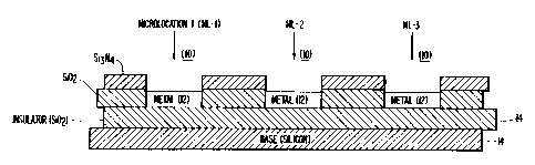
Figure 1 shows a basic design of self-addressable
micro-locations fabricated using microlithographic
techniques. The three micro-locations (10) (ML-1, ML-2,
ML-3) arc formed on the surface of metal sites (12) which
have been deposited on 'an insulator layer/base material(14).
The metal sites (12) serve as the underlying micro
electrode structures (10). An insulator material
separates the metal sites (12) from each other. Insulator
materials include, but are not limited to, silicon
dioxide, glass, resist, rubber, plastic, or ceramic
materials.
Figure 2 shows the basic features of an individual
micro-location (10) formed on a microlithographically
produced metal site (12). The addressable'micro-location
is formed ~ on the metal site (12 ) , and incorporates , an
oxidatior. layer (20), a permeation layer (22), an
CA 02504343 1994-10-26
19
attachment layer (24). and a binding entity layer (26).
The metal oxide layer provides a base for the covalent
coupling of the permeation layer. The permeation layer
provides spacing between the metal surface and the attach-
ment/binding entity layers and allows solvent molecules,
small counter-ions, and gases to freely pass to and from
the metal surface. The thickness of the permeation layer
for microlithographically produced devices can range from
approximately 1 nanometers (nm) to 10 microns (~cm), with
2 nm to 1 ~cm being the most preferred. The attachment
layer provides a base for the covalent binding of the
binding entities. The thickness of the attachment layer
for microhithographically produced devices~can range from
0.5 nm to 1 Vim, with 1 nm to 200 nm being the most
preferred. In some cases, the permeation and attachment
layers can be formed from the same material. The specific
binding entities are covalently coupled to the attachment
layer, and form the specific binding entity layer. The
specific binding entity layer is usually a mono-layer of
the specific binding molecules. However, in some cases
the binding entity layer can have several or even many
layers of binding molecules.
Certain design and functional aspects of the permea
tion and attachment layer are dictated by the physical
25~ (e.g., size and shape) and the chemical properties of the
specific binding entity molecules. They are also dictated
to some extent by the physical and chemical properties of
the reactant and ~analyte molecules, which will be
subsec,~uently transported and bound to the micro-location.
For example, oligonucleotide binding entities can be
attached to one type of micro-location surface without
causing a loss of the DC mode function, i.e., the
underlying micro-electrode can still cause the rapid free
field electrophoretic transport of other analyte molecules
to or from the surface to which the oligonucleotide
binding entities are attached. ::cwever, if large globular
CA 02504343 1994-10-26
protein binding entities (e. g., antibodies) are attached
to the same type of surface, they may effectively insulate
the surface and cause a decrease or a complete loss of the
DC mode function. Appropriate modification of the
5 attachment layer would have to be carried out so as to
either reduce the number of large binding entities (e. g.,
large globular proteins) or provide spacing between the
hinding entities on the surface.
The spacing between micro-locations is determined by
10 the ease of fabrication, the requirement for detector
resolution between micro-locations, and the number of
micro-locations desired on a device. However, particular
sgacings between micro-locations, or special arrangement
o~r geometry of the micro-locations is not necessary for
15 device- function, in that any combination of micro-
locations (i.e., underlying micro-electrodes) can operate
over the complete device area. Nor is it necessary to
enclose the device or confine the micro-locations with
dielectric boundaries. This is because complex electronic
2a field patterns or dielectric boundaries are not required
to selectively move, separate, hold, or orient specific
molecules in the space or medium between any of the elec-
trodes. The device accomplishes this by attaching the
specific binding molecules and subsequent analytes and
reactants~to the surface of an addressable micro-location.
Free field electrophoretic propulsion provides for the
rapid and direct transport of any charged molecule between
any and all locations on the device.
As the number of micro-locations increases beyond
several hundred, the complexity of the underlying cir
cuitry of the micro-locations increases. In this case the
micro-location grouping patterns have to be changed and
spacing distances increased proportionally, or multi-layer
circuitry can be fabricated into the basic device.
In addition to micro-locations which have been
addressed with specific binding entities, a device will
CA 02504343 1994-10-26
21
contain some un-addressed, or plain micro-locations which
serve other functions. These micro-locations can be used
to store reagents, to temporarily hold reactants or
analytes, and as disposal units for excess- reactants,
analytes, or other interfering components in samples.
Other un-addressed micro-locations can be used in combina-
tion with the addressed micro-locations to affect or
influence the reactions that are occurring at these
specific micro-locations. These micro-locations add to
intra-device activity and control. It is also possible
far the micro-locations to interact and transport
molecules between two separate devices. This provides a
mechanism for loading a working device with binding
entities or reactants from a storage device, and for
copying or replicating a device.
Figure 3 shows a matrix type device containing 64
addressable micro-locations (30). A 64 micro-location
device is a convenient design, which fits with standard
microelectronic chip packaging components. Such a device
is fabricated on a silicon chip substrate approximately
1.5 cm x 1.5 cm, with a central area approximately 750 ~m
x 750 ~m containing the 64~micro-locations. Each micro-
location (32) is approximately 50 ~.m square with 50 ~m
spacing between neighboring micro-locations. Connective
circuitry for each individual underlying micro-electrode
runs to an outside perimeter (10 mm x 10 mm) of metal
contact pads (300 um square) (34). A raised inner peri-
meter can be formed between the area with the micro-
locations and the contact pads, producing a cavity which
can hold approximately 2 to 10 microliters (~,l) of a
sample solution. The "chip" can be mounted in a standard
quad package, and the chip contact pads (34) wired to the
quad package pins. The packaged chip can then be plugged
into a microprocessor controlled DC power supply and
multimeter apparatus which can control and operate the
d°VlCe.
CA 02504343 1994-10-26
22
f'ABRI-CAT I ON PROD ",~~jE ~ ( M I CROL~ I3'~j,OGRAPHY )
~,Q~~S hoar~hy ~ab~i~~a~io~~"~teps
General microlithographic or photolithographic
techniques can be used for the fabrication of the complex
"chip° type device which has a large number of small
micro-locations. While the fabrication of devices does
not require complex photolithography, the selection of
materials and the requirement that an electronic device
function actively in aqueous solutions does require
l0 special considerations. .
The 64 micro-location device (30) shown in Figure 3
can be fabricated using relatively simple mask design and
standard microlithographic technic~ues.~ Generally, the
base substrate material would be a 1 to 2 centimeter
square silicon wafer or a chip approximately 0.5 milli-
meter in thickness. The silicon chip is first overcoated
with a 1 to 2 um thick silicon dioxide (SiO~) insulation
coat. Which is applied by plasma enhanced chemical vapor
deposition (PECVD).
In the. next step, a 0.2 to 0.5 ~m metal layer (e. g.,
aluminum) is deposited by vacuum evaporation. In addition
to aluminum, suitable metals for circuitry include gold,
silver, tin, copper, platinum, palladium, carbon, and
various metal combinations. Special techniques for
25- ensuring proper adhesion to the insulating substrate
materials (SiO~) are used with different metals.
The chip is next overcoated ,with a positive photo-
resist (Shipley, Microposit AZ 1350 J), masked (light
field) with the circuitry gattern, exposed and developed.
The photosolubilized resist is removed, and the exposed
aluminum is etched away. The resist island is now
removed, leaving the aluminum circuitry pattern on the
chip. Thia includes an outside perimeter of metal contact
pads, the connective circuitry (wires), and the center
array of micro-electrodes which serve as the underlying
base for the addressable micro-locations.
CA 02504343 1994-10-26
23
Using PECVD, the chip is overcoated first with a 0.2
to 0.4 micron layer of SiOz, and then with a 0.1 to 0.2
micron layer of silicon nitride (Si3N,). The chip is then
covered with positive photoresist, masked for the contact
pads and micro-electrode locations, exposed, and
developed. Photosolubilized resist is removed, and the
SiO~ and Si,N, layers are etched away to expose the aluminum
contact pads and micro-electrodes. The surrounding island
resist is then removed, the connective Wiring between the
l0 contact pads and the micro-electrodes remains insulated by
the SiOz and Si3N, layers .
The SiO~ and Si,N, layers provide important properties
for the functioning of the device. First, the second Si02
layer has better contact and improved sealing with the
aluminum circuitry. It is also possible to use resist
materials to insulate and seal. This prevents undermining
of the circuitry due to electrolysis effects when. the
micro-electrodes are operating. The final surface layer
coating of Si3N, is used because it has much less
reactivity with the subsequent reagents used to modify the
micro-electrode' surfaces for the attachment of specific
binding enti-ties.
c
At this point the micro-electrode locations on the
device are ready to be modified with a specialized permea-
tion and attachment layer. This represents the most
important aspect of the invention, and is crucial for the
active functioning of the device. The objective is to
create on the micro-electrode an intermediate permeation
layer with selective diffusion properties and an attach-
ment surface layer with optimal binding properties. The
attachment layer should have from 105 to 10' functionalized
locations per square micron (um~) for the optimal attach-
ment of specific binding entities. However, the
attachmert.of speci~ic binding entities must not overcoat
CA 02504343 1994-10-26
24
or insulate the surface so as to prevent the underlying
micro-electrode from functioning. A functional device
requires some fraction (-. 5% to 25% ) of the actual metal
micro-electrode surface to remain accessible to solvent
(HZO) molecules, and to allow the diffusion of counter-ions
(e.g. , Na' and Cl') and electrolysis gases (e.g. , Oz and H2)
to occur.
The intermediate permeation layer must also allow
diffusion-to occur. Additionally, the permeation layer
should have a pore limit property which inhibits or
impedes the larger binding entities, reactants, and
analytes from physical contact with the micro-electrode
surface. The permeation layer keeps the active micro-
electrode surface physically distinct from the binding
entity layer of the micro-location.
In terms of the primary device function, this design
allows the electrolysis reactions required for electro-
phoretic transport to occur on micro-electrode surface,
but avoids adverse electrochemical effects to the binding
entities, reactants, and analytes:
One preferred procedure for the derivatization of the
metal micro-electrode surface uses aminopropyltriethoxy
silane (APS). APS reacts readily with the oxide and/or
hydroxyl groups on metal and silicon surface. APS
provides a combined permeation layer and attachment layer,
with primary amine groups for the subsequent covalent
coupling of binding entities. In terms of surface binding
sites, APS produces a relatively high level of
functionalization (i.e., a large. number of primary amine
groups) on slightly oxidized aluminum surfaces, an inter-
mediate level of functionalization on SiOz surfaces, and
very limited functionalization of Si,N, surfaces.
The APS reaction is carried out by treating the whole
device (e.g. , a chip) surface for 30 minutes with a IO%
solution of APS in toluene at 50°C. The chip is then
washed in toluene, ethanol, and then dried for one hour at
CA 02504343 1994-10-26
50°C. The micro-electrode metal surface is functionalized
with a large wumber of primary amine groups ( 105 to 106 per
square micron). Binding entities can now be covalently
bound to the derivatized micro-electrode surface.
.5 The APS procedure works well for the attachment of
oligonucleotide binding entities. Figure 4 shows the
mechanism for the attachment of 3'-terminal aldehyde
derivatized oligonucleotides (40) to an APS functionalized
surface (42). While this represents one of the preferred
10 approaches, a variety of other attachment reactions are
possible for both the covalent and non-covalent attachment
of many types of binding entities.
DESIGN AND Fp~3RICATION (MICRO-MACHINING)
This section describes how to use micro-machining
15 techniques (e.g., drilling, milling, etc.) or non
lithographic techniques to fabricate devices. In general,
these devices have relatively larger micro-locations
(> 100 microns) than those produced by microlithography.
These devices could be used for analytical applications, .
20 as well as for preparative type applications, such as
biopolymer synthesis. Large addressable locations could
be fabricated in three dimensional formats (e.g., tubes or
cylinders) in order to carry a large amount of binding
entities. Such devices could be fabricated using a
25 variety of materials, including, but not limited to,
plastic, rubber, silicon, glass (e. g., microchannelled,
microcapillary, etc.), or ceramics. In the case of micro-
machined devices, connective circuitry and larger
electrode structures can be printed onto materials using
standard circuit board printing techniques known to those
skilled in the art.
Addressable micro-location devices can be fabricated
relatively easily using micro-machining techniques.
Figure 5 is a schematic of.a representative 96 micro-
location device. This micro-location device is fabricated
CA 02504343 1994-10-26
2b
from a suitable material stock (2 cm x 4 cm x 1 cm) , by
drilling 96 proportionately spaced holes (1 mm in diame-
ter) through the material. An electrode circuit board
(52) is formed on a thin sheet of plastic material stock,
which fit precisely over the top of the micro-location
component (54). The underside of the circuit board
contains the individual wires (printed circuit) to each
micro-location (55). Short platinum electrode.structures
(- 3-4 mm) (62) are designed to extended down into the
individual micro-location chambers (57). The printed
circuit wiring is coated with a suitable water-proof
insulating material. The printed circuit wiring converges
to a socket, which allows coruiection to a multiplex switch
controller (56) and DC power supply (58). The device is
partially immersed and operates in a common buffer
reservoir (59).
While the primary function of the micro-locations in
devices fabricated by micro-machining and microlithography
techniques is the same, their designs are different. In
devices fabricated by~microlithography, the permeation and
attachment layers are formed directly on the underlying
metal micro-electrode. In devices fabricated by 'micro-
machining techniques, the permeation and attachment layers.
are physically separated from their individual metal
electrode structure (62) by a buffer solution in the
individual chamber or reservoir (57) (see Figure 6). In
micro-machined devices the permeation and attachment
layers can be formed using functionalized hydrophilic
gels, membranes, or other suitable porous materials.
In general, the thickness of the combined permeation
and attachment layers ranges from 10 um to 10 mm. For
example, a modified hydrophilic gel of 26x to 35 ~t polya-
crylamide (with O.l~C polylysine), can be used to partially
fill (- 0.5 mm) each of the individual micro-location
chambers in the device. This concentration of gel forms
an ideal permeation layer with a pore limit of from 2 nm
CA 02504343 1994-10-26
27
to 3 nm. The polylysine incorporated into the gel pro-
vides primary amine functional groups for the subsequent
attachment of specific binding entities. This type of gel
permeation layer allows the electrodes to function
actively in the DC mode. When the electrode is activated,
the gel permeation layer allows small counter-ions to pass
through it, but the larger specific binding., entity
molecules are concentrated on the outer surface. Here
they become covalently bonded to the outer layer of
primary amines, which effectively becomes the attachment
layer.
An alternative technique for the,formation of the
permeation and attachment layers is to incorporate into
the base of each micro-location chamber a porous membrane
material. The outer surface of the membrane is then
derivatized with chemical functional groups to form the
attachment layer. Appropriate techniques and materials
for carrying out this approach are known to those skilled
in the art.
The above description for the design and fabrication
of a device should not be considered as a limit to other
variations or forms of the basic device. Many variations
of the device with larger or smaller numbers of address-
able micro-locations are envisioned for different analy-
tical and preparative applications. Variations of the
device with larger addressable locations are envisioned
for preparative biopolymer.synthesis applications, varia-
tions are also contemplated as electronically addressable
and controllable reagent dispensers for use with other
devices, including those produced by microlithographic
techniques.
(2) SELF-DIRECTED ADDRESSING OF THE DEVICES
The claimed devices are able to electronically self
address each micro-location with a specific binding
entity. The device itself directly affects or causes the
CA 02504343 1994-10-26
2e
transport and attachment of specific binding entities to
specific micro-locations. The device self-assembles
itself in the sense that no outside process, mechanism, or
equipment is needed to physically direct, position, or
'S place a specif is binding entity ~ at a specif is micro-
location. This self-addressing process is both rapid and
specific, and can be carried out in either a serial or
parallel manner.
A device can. be serially addressed with specific
binding entities by maintaining the selected micro
location in a DC mode and at the opposite charge (poten
tial) to that of a specific binding entity. A11 other
micro-locations are maintained at the same charge as the
specific binding entity. In cases where the binding
entity is not in excess of the attachment sites on the
micro-location, it is necessary to activate only one other
micro-electrode to affect the electrophoretic transport to
the specific micro-location. The specific binding entity
is rapidly transported (in a few seconds, or preferably
less than a second) through the solution, and concentrated
directly at the specific micro-location where it
immediately becomes covalently bonded to the special
surface. The ability to electronically concentrate
'reactants or analytes (70) on a specific micxo-location
(72) is shown in Figure 7. All other micro-locations
remain unaffected by that specific binding entity. Any
unreacted binding entity is removed by reversing the
polarity of that specific micro-location, and electro-
phoresing it to a disposal location. The cycle is
repeated until all desired micro-locations are addressed
with their specific binding entities. Figure 8 shows the
serial process for addressing specific micro-locations
(81, 83, 85) with specific oligonucleotide binding
entities (82, 84, 86).
The parallel process for addressing micro-locations
simply involves simultaneously activating a large number
CA 02504343 1994-10-26
29
(particular group or line) of micro-electrodes so that the
same specific binding entity is transported, concentrated,
and reacted with more than one specific micro-locations.
(3) APPLICATIONS OF THE DEVICES
Once a device has been self-addressed with specific
binding entities, a variety of molecular biology type
mufti-step and multiplex reactions and analyses can be
carried out on the device. The devices of this invention
are able to electronically provide active or dynamic
control over a number of important reaction parameters.
This electronic control leads to significant improvements
in reaction rates, specificities, and~sensitivities. The
improvements in these reaction parameters come from the
ability of the device to electronically control and
affect: (1) the rapid transport of reactants or analytes
to a specific micro-location containing attached specific
binding entities; (2) improvement in reaction rates due to
the concentrated reactants or analytes reacting with the
specific binding entities at that specific micro-location;
20~ and (3) the rapid and selective removal of un-reacted and
non-specifically bound components from that micro-loca-
tion. These advantages are utilized in a novel process
called "electronic stringency control".
The self-addressed devices of this invention are able
to rapidly carry out a variety of micro-formatted multi
step and/or multiplex reactions and procedures; which
include, but are not limited to:
- DNA and RNA hybridizations procedures and
analysis in conventional formats, and new
improved matrix formats;
~ molecular biology reaction procedures, ~.g.,
restriction enzyme reactions and analysis,
ligase reactions, kinasing reactions, and
amplification procedures;
CA 02504343 1994-10-26
- antibody/antigen reaction procedures involving
large or small antigens and haptens;
diagnostic assays, e.g., hybridization analysis,
gene analysis, fingerprinting, and immuno
5 diagnostics;
- biomolecular conjugation procedures (i.e. the
covalent and non-covalent labeling of nucleic.
acids, enzymes, proteins, or antibodies With
reporter groups);
10 - biopolymer synthesis procedures, e.g.,
combinatorial synthesis of oligonucleotides or
peptides;
- water soluble synthetic polymer synthesis, e.g.,
carbohydrates or linear polyacrylates; and
15 -~ macromolecular and nanostructure (nanometer size
particles and structures) synthesis and
fabrication.
NUCLEI_f;',P~CI~ HY8R1,~~?IZATION
Nucleic acid hybridizations are used as examples of
20 this invention because they characterize the most diffi
cult mufti-step and multiplex reactions.
The claimed device and methods allow nucleic acid
hybridization to be carried out in a variety of conven-
tional and new formats. The ability of the device to
25 electronically control reaction parameters greatly
improves nucleic acid hybridization analysis, particularly
the ability of the device to provide electronic stringency
control (ESC) .
By "nucleic acid hybridization" is meant hybridiza
30 tion between all natural and synthetic forms and deriva
tives of nucleic acids, including: deoxyribonucleic acid
(DNA), ribonucleic acid (RNA), polynucleotides and
oligonucleotides.
Conventional hybridization formats, such as "dot
blot" hybridization and "sandwich" hybridization, can be
CA 02504343 1994-10-26
31
carried out with the claimed device as well as large scale
array or matrix formats.
As an example, a device for DNA hybridization analy
sis is designed, fabricated, and used in the following
manner. Arrays of micro-locations are first fabricated
using microlithographic techniques. The number of
addressable micro-locations on an array depends on the
final use. The device is rapidly self-addressed in a
serial manner with a~ group of specif is oligonucleotides .
In this case, the specific oligonucleotides are 3'-
terminal aldehyde functionalized oligonucleotides (in the
range of 6-mer to 100-mer). The aldehyde functional group
allows for covalent attachment to the specific micro-
location attachment surface (see Figure 4). This group of
specific oligonucleotides can be readily synthesized on a
conventional DNA synthesizer using conventional tech-
niques.
The synthesis of each specific oligonucleotide is
initiated from a ribonucleotide controlled pore glass
(CPG) support. Thus, the 3'-terminal position contains a
ribonucleotide, which is then easily converted after
synthesis and purification to a terminal dialdehyde
derivative by periodate oxidation. The aldehyde
containing oligonucleotides (40) will react readily with
the primary amine functional groups on the surface of
micro-locations by a Schiff's base reaction process.
The electronic addressing of the device with specific
oligonucleotides is shown in Figure 8. The addressing of
the first specific micro-location (ML-1) (el) with its
specific sequence oligonucleotide (SSO-1) (82) is accom-
plished by maintaining the specific microelectrode (ML-1)
at a positive DC potential, while all other microelec-
trodes are maintained at a negative potential (Fig. 8(A)).
The aldehyde functional.ized specific sequence (SSO-1) in
aqueous buffered solution is free field electrophoresed to
the I~L-1 address, where it concentrates (> la6 fold) and
CA 02504343 1994-10-26
32
immediately becomes covalently bound to the surface of ML-
1 (81). All other microelectrodes are maintained nega-
tive, and remain protected or shielded from reacting with
SSO-1 sequence (82). The ML-1 potential is then reversed
to negative (-) to electrophores any~unreacted SSO-1 to a
disposal system. The cycle is repeated, SSO-2 (84) --->
ML-2 (83), SSO-3 (86) ---> ML-3 (85), SSO-n ---> ML-n
until all the desired micro-locations are addressed with
their specif is DNA sequences (Fig. 8(D)).
ZO Another method for addressing the device is to trans-
port specific binding entities such as specific oligonu-
cleotides from an electronic reagent supply device. This
supply device would hold a large quantity of binding
entities or reagents and would be used to load analytical
devices. Binding entities would be electronically trans-
ported between the two devices. Such a process eliminates
the need for physical manipulations, such as pipetting, in
addressing a device with binding entities.
Yet another method for addressing the device is to
carry out the combinatorial synthesis of the specific
oligonucleotides at the specific micro-locations.
Combinatorial synthesis is described in a later section.
After the device is addressed with specific DNA
sequences, the micro-locations on the array device remain
25~ as independent working direct current (DC) electrodes.
This is possible because the attachment to the electrode
surface is carried out in such a manner that the underly-
ing micro-electrode does not become chemically or physi-
cally insulated. Each micro-electrode can still produce
the strong direct currents necessary for the free field
electrophoretic transport of other charged DNA molecules
to and from the micro-location surface. The DNA array
device provides complete electronic control over all
aspects of the DNA hybridization and any other subsequent
reactions.
CA 02504343 1994-10-26
33
An example of an electronically controlled hybridiza-
tion process is shown in Figure 9. In this case, each
addressable micro-location has a specific capture sequence
(90). A sample solution containing target DNA (92) is
applied to the device. All the micro-locations are acti-
vated and the sample DNA is concentrated at the micro-
locations (Fig. 9(H)). Target DNA molecules from the
dilute solution become highly concentrated at the micro-
locations, allowing very rapid hybridization to the
specific complementary DNA sequences on the surface.
Reversal of the micro-electrode potential repels all un-
hybridized DNA from the micro-locations, while the target
DNA remains hybridized (Fig. 9(C)). In similar fashion,
reporter probes are hybridized in subsequent steps to
detect hybridized complexes.
The electronic control of the hybridization process
significantly improves the subsequent detection of the
target DNA molecules by enhancing the overall hybridiza-
tion efficiency and by removing non-specific DNA from the
micro-location areas. It is expected that 10.,000 to
100,000 copies of target sequences in un-amplified genomic
DNA will be detectable. Hybridization reactions ~of this
type can be carried out in a matter of minutes, with
minimal outside manipulations. Extensive washing is not
necessary.
Another common format for DNA hybridization assays
involves having target DNAs immobilized on a surface, and
then hybridizing specific probes to these target DNAs.
This format can involve either the same target DNAs at
multiple locations, or different target DNAs at specific
locations . Figure 10 shows an improved version of this
serial hybridization format. In this case micro-locations
(101-107) are addressed with different capture DNAs.
These are hybridized in a serial fashion with different
sequence specific oligonucleotides (108,109). The micro-
locations_are sequentially biased positive to transport
CA 02504343 1994-10-26
34
molecules to itself and then biased negative to transport
molecules to the next micro-location. Specifically
hybridized DNA will remain at the micro-location
regardless of electrode potential. The sequence specific
oligonucleotides can be labeled with a suitable reporter
group such as a fluorophore.
The claimed device is able to provide electronic
stringency control. Stringency control is necessary for
hybridization specificity, and is particularly important
for resolving one base mismatches in point mutations.
Figure 11 shows how electronic stringency control can be
used for improving hybridization specificity for one base
mismatch analysis. The electronic stringency control can
also be applied to multiple-base mismatch analysis.
Perfectly matched DNA hybrids ( 110 ) are more stable
than mismatched DNA (112) hybrids. By biasing the micro-
locations negative (Fig. 11(B)) and delivering a defined
amount of power in a given time, it is possible to
denature or remove the mismatched DNA hybrids while
retaining the perfectly matched DNA hybrids (Fig. 11(C)).
In a further refinement, the claimed device provides inde-
pendent stringency control to each specific hybridization
reaction occurring on the device. With a conventional or
passive array format, it is impossible to achieve optimal
stringency for all the hybridization events which are
occurring in the same hybridization solution. However,
the active array devices of this invention are able to
provide different electronic stringency to hybridizations
at different .micro-locations, even though they are
occurring in the same bulk hybridization solution. This
attribute overcomes a major limitation to conventional
matrix hybridization formats, sequencing by hybridization
(SBH) formats, and other multiplex analyses.
The ability to provide electronic stringency control
to hybridizations also provides mechanisms for detecting
DNA hybridization without reporter group labeled DNA
CA 02504343 1994-10-26
probe. It provides a way to carry out a more direct
detection of the hybridization process itself. A fluore-
scent dye detection process is shown in Figure l2 and
described in Examples 4 and 6. Direct detection of DNA
5 hybrids can be achieved by using DNA binding dyes such as
ethidium bromide. The dye binds to both double-stranded
and single-stranded DNA but with a greater affinity for
the former. In Figure 12(B) positively charged dye (122)
is transported to negatively biased micro-locations. The
10 dye binds to both hybridized (120) and unhybridized (121)
DNA sequences (Fig. 12c). By biasing the micro-locations
positive and delivering a defined amount of power in a
given amount of time, the dye molecules bound to
unhybridized micro-locations is selectively removed. The
15 amount of power applied does not adversely affect the DNA
hybrids.
The hybridized DNAs with associated dye molecules are
then fluorescently detected using associated or integrated
optical systems.
20 The following reiterates the important advantages the
devices of this invention provide for nucleic acid hybridi-
nation reactions and analysis:
(1) The rapid transport of dilute target DNA and/or
probe DNA sequences to specific micro
25 locations) .where hybridization is to occur.
This process takes place in no more than a f.ew
seconds.
' (2) Concentrating dilute target DNA and/or probe DNA
sequences at specific micro-locations) where
30 hybridization is to occur. The concentrating
effect can be well over a million fold (> 106).
(3) The rapid removal of non-specifically bound
target DNA sequences from specific micro
location(s) where hybridization has occurred.
35 , This process takes 10 to 20 seconds.
CA 02504343 1994-10-26
3s
(4) Rapid removal of competing complementary target
DNA sequences from specific micro-locations)
where hybridization has occurred. This process
takes 10 to 20 seconds.
(s) The ability to carry out a complete hybridization
process in several minutes.
(7) The ability to carry out a hybridization process
with minimal outside manipulations or washing
steps.
(8) The use of electronic stringency control (ESC) to
remove partially hybridized DNA sequences.
(~9) The ability to carry out hybridization analysis
of un-amplified genomic target DNA sequences in
the 1000~to 100,000 copy range.
(10) The use of ESC to improve the resolution of
single base mis-match hybridizations (point
mutations).
(11) The use of ESC to provide individual stringency
control in matrix hybridizations.
(12) Improving the detection of hybridization event
by removing non-specific background components.
(13) The development of new procedures which.elimi
nate the need for using covalently labeled
reporter probes or target DNA to detect the
hybridization events.
REPRODUCTION OF DEVICES
In addition to separately addressing individual
devices with specific binding entities, it is also pos-
sible to produce a master device, which can copy specific
binding entities to other devices. This represents
another method for the production of devices. The process
for the replication of devices is shown in Figure'13. A
master device containing micro-locations which have been
addressed with specific binding sequences is hybridized
with respective complementary DNA sequences (130). These
CA 02504343 1994-10-26
37
complementary sequences are activated and thus capable of
covalent binding to the micro-location attachment layer.
An unaddressed sister device (132) containing an
attachment layer is aligned with the hybridized master
device (Fig. 13(B)). The master device micro-locations
are biased negative and the sister device micro-locations
are biased positive. The DNA hybrids are denatured and
are transported to the sister device, where the activated
DNA sequence binds covalently to the micro-location
(Fig. 13(C)). The process can be performed in parallel or
in series, depending on the device geometry so that
crosstalk between the micro-locations is minimized. The
hybrids can be denatured by applying a sufficient negative
potential or by using a positively charged chaotropic
agent~or denaturant.
DIETECTIQ]~ S~ST~,f~
In the case of fluorescent binding reactions, it is
possible to use an epifluorescent type microscopic detec-
tion system for the analysis~of the binding reactions.
The sensitivity of the system depends on the associated
imaging detector element (CCD, ICCD, Microchannel Plate)
or photon counting PMT system. One alternative is to
associate a sensitive CCD detector or avalanche photodiode
(APD) detector directly with the device in a sandwich
arrangement. Another alternative is to integrate opto-
electronic or microelectronics detection in the device.
COMB I NATOR I AL B I O,pOLYMER. ~yS I S
The devices of this invention are also capable of
carrying out combinatorial synthesis of biopolymers such
as oligonucleotides and peptides. Such a process allows
self-directed synthesis to occur without the need for any
outside direction or influence. This combinatorial syn-
thesis allows very large numbers of sequences to be
synthesised on a device. The basic concept for combina-
CA 02504343 1994-10-26
38
torial synthesis involves the use of the device to trans-
port, concentrate, and react monomers, coupling reagents,
or deblocking reagents at the addressable micro-locations.
The concept capitalizes on the ability of the device to
protect certain locations from~the effects of nearby
reagents. Also important to the concept is the identifi-
cation of selective steps in these chemical synthesis
processes where one or more of the reactants has either a
net positive or negative charge, or to create such
suitable reagents for these processes.
One method for combinatorial oligonucleotide synthe-
sis is shown in Figure 14. This method begins with a set
of selectively addressable micro-locations (140) whose
surfaces have been derivatized with blocked primary amine..
(X-NH-) groups (142). The initial step in the process
involves selective deblocking of electrodes using a
charged deblocking reagent (144). In this case, the
reagent would carry a positive (+) charge. The process is
carried out by applying a negative potential to those
electrodes being de-blocked, and a positive potential~to
those which are to remain protected (Fig. 14(B)).
Application of positive and negative potentials to
selective electrodes causes the charged reagents to be
concentrated at those micro-locations being de-blocked,
and excludes the reagents from the other electrode
surfaces.
In the second step, chemical coupling of the first
base, in this case cytosine, to the deblocked micro-
locations is carried out by simply exposing the system to
the phosphoramidite reagent (x-C) (146). The (C)
nucleotide couples to de-blocked micro-location surfaces,
but not to any of the blacked electrode surfaces
(Fig. 14(C) and (D)). At this point normal phosphoramide
chemistry IS carried out until the next de-blocking step.
At the second de-blocking step (Fig. 14(D)), those
electrode positions which are to be coupled with the next
CA 02504343 1994-10-26
39
base are made negative, and those which are to remain
protected are made positive. The system is now exposed to
the next base to be coupled, in this case (x-A) (148), and
selective coupling to the de-blocked micro-location is
achieved (Fig. 14(E) and (F)). The coupling and de-
blocking procedures are repeated, until all the different
DNA sequences have been synthesized on each of the
addressable micro-location surfaces.
The above example represents one possible approach
for the synthesis of nucleic acids. Another approach
involves a complete water soluble DNA synthesis. In this
case, charged water soluble coupling agents, such as 1
ethyl-3-(3-dimethylaminopropyl) carbodiimide (EDCA), is
used to carry out oligonucleotide synthesis with water
soluble nucleotide derivatives. This approach would have
significant advantages over present organic solvent based
methods which require extensive blocking of the base
moieties. Water soluble synthesis would be less expensive
and eliminate the use of many toxic substances used in the
present organic solvent based processes. A third approach
involves the use of charged monomers.
In addition to DNA synthesis, a similar process can
be developed for peptide synthesis, and other complex
'polymers. Examples contemplated in this disclosure
represent the initial potential for this technique, and
are based on organic solvent based synthetic procedures
for DNA or peptide synthesis.
The recipes for buffers, solutions, and media in the
following examples are described in J. Sambrook, E. F.
Fritsch, and T. Maniatis, Molecular Clonina: A Laboratory
ua , 2 Ed., Cold Spring Harbor Laboratory Press, Cold
Spring Harbor, New York, 1989.
Example 1: Oliaomer Rea e~nt_s,
Synthetic DNA probes were made using conventional
phosphoramidite chemistry on Applied Biosystems automated
CA 02504343 1994-10-26
DNA synthesizers. Oligomers were designed to contain
either a 5' amino or a 3' ribonucleoside terminus. The 5'
functionality was incorporated by using the ABI Aminolink
2 reagent and the 3' functionality was introduced by initi-
5 sting synthesis from an RNA CPG support. The 3'
ribonucleotide terminus can be converted to a terminal
dialdehyde by the periodate oxidation method which can
react with primary amines to form a Schiff's base. Reac-
tion conditions were as follows:~Dissolve 20-30 O.D.
10 oligomer in water to a final concentration of 1 OD/~1.
Add 1 vol of O.1M sodium acetate, pH 5.2 and 1 vol 0.45M
sodium periodate (made fresh in water) . . Stir and incubate
reaction for at least 2 hours at ambient temperature, in
the dark. Load reaction mix onto a Sephadex G-10 column
15 (pasteur pipette, 0.6 .X 5.5 cm) equilibrated in O.1M
sodium phosphate, pH 7.4. Collect 200 ~cl fractions, spot
2 ~1 aliquots on thin layer chromatography (TLC) and pool
ultra violet (UV) absorbing fractions.
The following oligomers contain 3' ribonucleoside
20 termini' (U)
ET12R 5'- GCT AGC CCC TGC TCA TGA GTC TCU
CP-1 5'- AAA AAA AAA AAA AAA AAA AAU
AT-A1 5'- CTA CGT GGA CCT GGA GAG GAA GGA GAC TGC CTG U
AT-A2 5'- GAG TTC AGC AAA TTT GGA GU
25 AT-A3 5'- CGT AGA ACT CCT CAT CTC CU -
AT-A4 5'- GTC TCC TTC CTC TCC AGU
AT-A5 5-'- GAT GAG CAG TTC TAC GTG GU
AT-A6 5'- CTG GAG AAG AAG GAG ACU
AT-A7 5'- TTC CAC AGA CTT AGA TTT GAC U
30 AT-AS 5'- TTC CGC AGA TTT AGA AGA TU
AT-A9 5'- TGT TTG CCT GTT CTC AGA CU
AT-A10 5'- CAT CGC TGT GAC AAA ACA TU
Oligomers containing 5' amine groups were generally
reacted with fluorophores, such as Texas Red (TR, ex.
35 590nm, em. 610nm). Sulfonyl chlorides are very reactive
towards primary amines forming a stable sulfonamide
CA 02504343 1994-10-26
41
linkage. Texas Red-DNA conjugates were made as follows:
Texas Red Probes) was
sulfonyl
chloride
(Molecular
dissolved in dimethyl formamide (DMF) to a final
concentration was dissolved
of 50
mg/ml
(80 mM).
Oligomer
in 0.4M sodium bicarbonate, pH 9.0-9.1,to a final
concentra tion of 1 O.D./~C1 (5.4 for a
mM 21-mer)
.
In
a
micro tes t tube, 10 ~ul oligomer ~tl Texas Red was
and 20
combined. Let reaction proceed in the dark
for
1
hour.
Quench action with ammonia or
re hydroxylamine, lyophilize
10sample et 1989, supra).
and purify al.,
by PAGE
(Sambrook
The following oligomerswcontain ami no termini:
5'
ET21A 5'- Aminolink2 - TGC GAG CTG CAG TCA GAC AT
ET10AL 5'- Aminolink2 - GAG AGA CTC ATG AGC AGG
ET11AL 5'- Aminolink2 - CCT GCT CAT GAG TCT CTC
15T2 5'- Aminolink2 - ~TTT TTT TTT TTT TTT TTT TT
RC-A1 5'- Aminolink2 - CAG GCA GTC TCC TTC CTC TCC AGG
TCC ACG
TAG
RC-A2 5'- Aminolink2 - CTC CAA ATT TGC TGA ACT C
RC-A3 5'- Aminolink2 - GGA GAT GAG GAG TTC TAC G
20RC-A4 S'- Aminolink2 - CTG GAG AGG AAG GAG AC
RC-A5 5'- Aminolink2 - CCA CGT AGA ACT GCT CAT C
RC-A6 5'- Aminolink2 - GTC TCC TTC TTC TCC AG
RC-A7 5'- Aminolink2 - GTC AAA TCT AAG TCT GTG GAA
RC-A8 5'- Aminolink2 - ATC TTC TAA ATC'TGC GGA A
25RC-A9 5'- Aminolink2 - GTC TGA GAA CAG GCA AAC A
RC-A10 5'- Aminolink2 - ATG TTT TGT CAC AGC GAT G
Example 2: Electronically Addressable Micro-locations
on a Microfabricat~d Device Polylvsine
Method
30 Microelectrodes were fabricated from microcapillary
tubes (0.2 mm x 5 mm). The microcapillaries were filled
with 18-26% polyacrylamide containing 0.1 - 1.0% goly-
lysine and allowed to polymerize. The excess capillary
was scored and removed to prevent air bubbles from being
35 trapped within the tubes and to standardize the tube
CA 02504343 1994-10-26
42
length. Capillaries were mounted in a manner such that
they shared a common upper buffer reservoir and had
individual lower buffer reservoirs. Each lower buffer
reservoir contained a platinum wire electrode.
The top surface of the microcapillary in the upper
reservoir was considered to be the addressable micro-
location. Upper and lower reservoirs were filled with
0.1 M sodium phosphate, pH 7.4 and prerun for 10' at 0.05
mA constant using a BioRad 500/1000 power supply. Pipette
2 ~C1 ( 0 .1 O. D . ) periodate oxidized ET12R into the upper
reservoir while the power is on and electrophorese for 2-5
minutes at constant current, Reverse polarity so that the
test capillary is now biased negative and~electrophorese
an additional 2-5 minutes. Unbound DNA is repulsed while
the covalently attached DNA remains.
Aspirate upper reservoir buffer and rinse with
buffer. Disassemble apparatus and mount a fresh reference
capillary. Refill reservoir and add fluorescently labeled
complement DNA, i.e., ETIOAL-TR. Electrophoretically
concentrate the oligomer at the positively biased test
micro-location for 2-5 minutes at 0.05 mA constant.
Reverse the polarity and remove unbound complement. Remove
test capillary and examine by fluorescence. Negative w
control for nonspecific binding was performed as described
25' above substituting a noncomplementary DNA sequence ET21A-
TR for ET10AL-TR.
A cross-section of the capillary micro-locations were
examined under a Jena epifluorescent microscope fitted
with a Hamamatsu ICCD camera imaging system. Fluorescent
results indicate that complement ET10AL-TR hybridized to
the binding entity/capture sequence and remained
hybridized even when the potential was changed to
negative. ET21A-TR noncomplement was not retained at the
test capillary when the potential was reversed.
CA 02504343 1994-10-26
43
Example 3: El,~c~ronicallv Addressable Micro-locations
on a Micr~~ ricated Device - Succinimidvl
gc~yrlatg Method
This example describes an alternative attachment
chemistry which covalently binds the 5' terminus of the
oligomer. Capillaries were fabricated as described above
except that 1% succinimidyl acrylate (Molecular Probes)
was substitute for the polylysine. The capillaries were
made fresh because the succinimidyl ester reacts with
primary amines and is labile, especially above pH 8Ø
The capillaries were mounted as described above and the
reservoirs were filled with 0.1 M sodium phosphate, pH
7.4. Prerun the capillaries for 10 minutes at 0.05 mA.
Pipette 2 ~1 ET10AL (0.1 O.D.), which contains a 5' amino
terminus, into the upper reservoir while the power is on
and electrophorese for 2-5 minutes. Reverse polarity so
that the test capillary is now biased negative and elec-
trophorese an additional 2-5 minutes. Unbound DNA is
repulsed while the covalently attached DNA remains.
Aspirate upper. reservoir buffer and. rinse with
buffer. Unmount the reference capillary and mount a fresh
reference capillary. Refill reservoir and add fluorescent
labeled complement oligomer, ET11AL-TR and electrophoreae
as described above. Negative control for nonspecific
binding was performed as described above substituting a
noncomplement DNA sequence ET21A-TR for ETilAL-TR.
Fluorescent results indicate that complement ET11AL-
TR hybridized to the capture sequence and remained
hybridized even when the potential was changed to
negative. ET21A-TR noncornplement was not retained at the
working capillary when the potential was reversed.
Example 4: Electronically CQ_n~ollo~escP,~nt Dve
Detecl~ioa Procgs~,-PAGE
DNA dyes such as ethidium bromide (E8) become fluore-
scent whey intercalated into Dl'~A. The fluorescence an3
CA 02504343 1994-10-26
44
binding affinity is greater when the DNA is double
stranded than single stranded. Prepare capillaries as in
Example 1 and hybridize as described above. EB was added
to the solution (- 0.05 mM EB final concentration) and the
test capillary was biased negative because EB is posi-
tively charged. The capillaries were observed by epifluor-
escence at 550 nm excitation and 600+ nm emission. Both
the hybridized and unhybridized micro-locations showed red
fluorescence (from EB)..
The capillaries were re-mounted biased positive to
repulse EB. Maintain constant current at 0.05 mA for 0.03
Volt-Hours.
Capture Target Normalized Signal
ET10AL ET11AL (Pos.) >200
ETlOAL ET21A (Neg.) 1
Fluorescence at the unhybridized micro-locations
diminished while the hybridized capillary retained fluore-
scence. Fluorescent signal was measured using an ICCD
camera imaging system and represent peak fluorescent
intensities. The signal to noise ratio would be »1000
fold if the entire fluorescent signal area was integrated.
This demonstrates a method for increasing signal to noise
ratios and thus the dynamic range of the assay.
Example 5: EleclG,~~onically Addressable Locati~,s on_
Metal Substrates
Aluminum (A1 ) and gold (Au) wire ( 0 . 25 mm, Aldrich)
was reacted with 10% 3-aminopropyltriethoxysilane (APS) in
toluene. The APS reagent reacts readily with the oxide
and/or hydroxyl groups on the metal surface to form cova-
lent bonds between the oxide and/or hydroxyl groups and
the primary amine groups. No pretreatment of the aluminum
was.necessary. The gold wire was subjected to electrolysis
in 5 x SSC solution to foam an oxide layer. Alternatively
the metal wire can be oxidized by a perchloric acid bath.
CA 02504343 1994-10-26
The APS reaction was performed as follows:. Wires
were cut to 3 inches and placed in a glass dish. Toluene
was added to completely cover the wires and the tempera-
ture was brought to 50-60 °C on a heat plate. APS was
.5 added to a final concentration of~l0%. Mix solution and
continue the reaction for 30 minutes. Rinse 3 times with
copious volumes of toluene, then rinse 3 times with
copious volumes of alcohol and dry in 50°C oven. The APS
treated wire can then be reacted with an aldehyde to form
10 a Schiff~s base. Binding entity ET12R was periodate
oxidized as described elsewhere. The electrodes were
placed in a reservoir of degassed water. Power Was applied
at .05 mA constant for about 30 seconds. Activated ET12R
was immediately added. Power was applied, the liquid was
15 aspirated and fresh water was added and then aspirated
again, The test (biased positive) and reference elec-
trodes were placed in Hybridization Buffer (H8, SXSSC,
0.1% SDS) containing fluorescent labeled complement DNA,
ET10-TR. After 2 minutes the electrodes were washed three
20 times for one minute each in Wash Buffer (1 x SSC, 0.1%
SDS) and observed by fluorescence (ex. 590 nm, em.
610 nm).
Results demonstrate that ET12R was specifically
coupled to the treated metal surfaces. The test electrode
25 was fluorescent while .the reference electrode was not.
Nonspecific adsorption of the DNA to the metal was
prevented by the presence of SDS in the Hybridization
Buffer. Attachment to gold substrates by electrolysis and
subsequent APS treatment was effective. Signal obtained
30 was significantly stronger than observed with non-oxidized
gold. More importantly, this example showed that the
metal surfaces could be chemically functionalized and
derivatized with a binding entity and not become insulated
from the solution. The APS method represents one of many
35 available chemistries to form DNA-metal conjugates.
CA 02504343 1994-10-26
46
Example 6:
~~~e~~io~g~ocess - Metal Wire
DNA-aluminum electrode substrates were prepared and
hybridized as described in Example 5. A hybridized and an
unhybridized DNA-A1 electrode were processed with' an
underivatixed A1 wire as the reference. EB was added to
the solution and the test DNA electrodes were biased
negative to attract the dye. The solution was aspirated
and fresh buffer was added. The metal surfaces were
to examined under the microscope.
Remount the device and apply a positive potential for
a defined volt-hour. The buffer was aspirated, the elec-
trodes were observed by epifluorescence. This was
repeated until there was a significant difference in
fluorescence between the hybridized and unhybridized metal
surfaces.
Capture Target Normalized Signal
ET12R ET10AL (Pos.) >140 .,
ET12R None (Neg. ) 1
Fluorescence at the unhybridized metal surfaces
diminished while the hybridized metal surfaces retained
fluorescence. Fluorescent signal was measured using an
ICCD camera imaging system and represent peak fluorescent
intensities. The signal to noise ratio would be a>100~0
fold if the entire fluorescent signal area was integrated.
This example demonstrates a method for increasing signal
to noise ratios and thus the dynamic range of the assay.
Similar results were obtained using capillary gel configu-
ration, suggesting that electrochemical effects do not
significantly affect the performance of the assay.
Example 7: Active ~roa~am~~ Electronic Matrix
(APEX) Micro-maghine_ ~~~icatio~~.
A radial array of 6 addressable 250 ~,m capillary
locations was micro-machined. The device has a common
upper reservoir and separate lower reservoirs such that
CA 02504343 1994-10-26
47
the potential at each micro-location is individually
addressable. A unique oligomer binding entity is localized
and coupled to a specific capillary micro-location by the
methods described elsewhere. The test micro-location has
a positive potential while the other micro-locations have
negative potentials to prevent nonspecific interactions.
The array is washed and then hybridized with a
complementary fluorescently labeled DNA probe. The array
is washed to remove excess probe and then observed under
an epifluorescent microscope. Only the specifically
addressed micro-location will be fluorescent. The process
will be repeated with another binding entity at another
location and verified by hybridization with a probe
labeled with another fluorescent moiety.
DNA sequences are specifically located to predeter-
mined positions with negligible crosstalk with the other
locations. This enables the fabrication of micromatrices
with several to hundreds of unique sequences at predeter-
mined locales.
Example 8: Active. Prog,~~m
An 8 X 8 matrix of 50 ~.m square aluminum electrode
pads on a silicon wafer (see Figure 3) was designed,
fabricated arid packaged with a switch box (see Device
Fabrication Section for details). Several materials and
process improvements, as described below, were made to
increase the selectivity and effectiveness of the chip.
8a) Selection_ of Togcoat
The APS process involves the entire chip. Selecti
vity of the functionalization process was dependent on the
reactivity of the chip surfaces. In order to reduce func
tionalization and subsequent DNA attachment of the areas
surrounding the micro-locations, a material that is less
reactive to APS than SiO~ or metal oxide is needed. Photo
CA 02504343 1994-10-26
4s
resists and silicon nitride were tried. The different
topcoats were applied to silicon dioxide chips. The chips
were examined by epifluorescence and the then treated with
APS followed by covalent attachment of periodate oxidized
'S polyA RNA sequences (Sigma, MW 100,000). The chips were
hybridized with 200 nM solution of Texas Red labeled 20
mer (T2-TR) in Hybridization Buffer, foz 5 minutes at 37°C.
The chips were washed 3 times in WB and once in 1 x SSC.
The chips were examined by fluorescence at 590 nm excita
tion and 610 nm emission.
Silicon nitride was chosen because it had much less
reactivity to APS relative to silicon dioxide and was not
inherently fluorescent like the photoresist tested. Other
methods such as W burnout of the background areas are
also possible.
8b ) P~PEX Phvs is~,~ (''~rtgr3T~,t i on
A finished matrix chip was visually examined using a
Probe Test Station (Micromanipulator Model 6000) fitted
with a B & L microscope and a CCD camera. The chip Was
tested for continuity between the test pads and the outer
contact pads. This was done by contacting the pads with
the manipulator probe tips which were connected to a
multimeter. Continuity ensures that the pads have been
etched down to the metal surface. The pads were then
checked for stability in electrolytic environments. The
metal wires were rated to handle up to 1 mA under normal
dry conditions. However, reaction to a wet environment
was unknown. A drop (1-5 ~l) of buffered solution (1 x
SSC) was pipetted onto the 8X8 matrix. Surface tension
keeps the liquid in place leaving the outer contact pad
area dry. A probe tip was contacted to a contact pad and
another probe tip was contacted with the liquid. The
current was incremented up to 50 nA at maX voltage of 50
V using a HP 6625A power supply and HP3458A digital
multimeter.
CA 02504343 1994-10-26
49
The initial fabrication consisted of the silicon
substrate, a silica dioxide insulating layer, aluminum
deposition and patterning, and a silicon nitride topcoat.
These chips were not very stable in wet environments
because the metal/nitride interface was physical 'in nature
and electrolysis would undermine the nitride layer. This
would result in the pads~being electrically shorted.
Furthermore, silicon nitride and Al have different expan-
sion coefficients such that the nitride layer would crack
when current was applied. This would allow solution to
contact the metal directly, again resulting in electrol-
ysis which would further undermine the layer.
The second fabrication process ~iricluiied a silicon
dioxide insulating layer between the aluminum metal and
silicon nitride layers. Silicon dioxide and Al have more
compatible physical properties and form a better chemical
interface to provide a more stabile and robust chip.
8c) DNA-A~~taShment
A matrix chip,was funct,ionalized with APS reagent as
~ described in Example 5. The chig was then treated with
periodate oxidized polyA RNA (Sigma, average Mt~1 100,000).
The chip was washed in WB to remove excess and unbound
RNA. This process coated the entire chip with the capture
'sequence with a higher density at the exposed metal
surfaces than at the nitride covered areas. The chip was
hybridized with a 200 nM solution of T2-TR in HB for 5
minutes at 37°C. Then washed 3 times in WB and once in
1XSSC for one minute each at ambient temperature. The
chip was examined by fluorescence at 590 nm excitation and
610 nm emission.
The opened metal areas were brightly fluorescent and
had the shape of the pads. Low fluorescent intensities
and/or irregular borders would suggest that the pads were
not completely opened. Additional plasma etch times would
be recommended.
CA 02504343 1994-10-26
8d) Elect~Qni~a,~~y Controlled Hyb~i~lization
Active hybridization was performed by using a chip
from~Example Sc and biasing one micro-location positive.
This was done by using the switch box which would also
5 automatically bias the remaining micro-locations negative
or by using an external solution electrode. Three micro-
liters of water was deposited on the matrix pads only. A
current, -1-5 nA, was applied for several seconds and 0.1
pmole of T2-TR was added to the solution. The liquid was
l0 removed and the chip was dried and examined by
fluorescence at Texas Red wavelengths (ex.590 nm, em.610
nm) .
Only the positively biased micro-location was
fluorescent. This can be repeated many times to hybridize
15 other micro-,locations selectively. Additionally, the
fluorescence DNA at one micro-location can be translocated
to another micro-location by biasing the initial location
negative and the destination positive.
8e) v'
20 ~albrication
The matrix was functionalized wi-th APS as described
above. Binding entity CP-1 was activated by periodate
oxidation method. Four micro-locations were biased posi-
tive in the matrix and the remainder were biased negative.
25 Two microliters of water was deposited on the matrix and
a current was applied. Binding entity, CP-1, was added
and allowed to concentrate at the designated locations.
The liquid was removed, the chip was rinsed briefly with
water and two microliters of water was deposited on the
30 chip. Again, current was applied for several seconds and
0.1 pmole of T2-TR was added. The liquid was removed
after a short time and the entire chip Was washed in WB,
3 times. The chip was dried and examined for
fluorescence.
CA 02504343 1994-10-26
51
Results indicate that the positively biased micro-
locations were fluorescent. This example demonstrates the
selective addressing of micro-locations with a specific
binding entity, the localization and covalent coupling of
sequences to the micro-locations, and the specific hybridi-
zation of complementary target sequences to the deriva-
tized micro-locations.
8f) Genetic , ina APEX Chin
DNA binding entities with 3' ribonucleoside termini
are synthesized which are specific for the polymorphisms
of HLA gene dQa. The binding entities are activated by
periodate oxidation as described above. The reverse
complements are also synthesized with 5' amino termini and
are conjugated with fluorophores, such as Texas Red,
Rhodamine or Bodipy dyes, as described elsewhere. The
micro-locations are functionalized with primary amines by
treatment with APS, as described elsewhere. A couple
microliters of solution are placed over the matrix but
leaving the contact pads dry. A specific micro-location
is addressed by biasing that micro-location positive, the
periodate oxidized DNA oligomer is added, ~0.1 pmole, and
is translocated and covalently coupled to that location.
The polarity is reversed and the unbound binding entity
molecules are removed. This is repeated for another
binding entity at another addressed micro-location until
all the unique binding entities are bound to the chip.
The chip is then hybridized to individual fluorescently
labeled complement sequences to determine the specificity
of the coupling reaction as well as en masse to visualize
all addressed micro-locations at once. On the same chip
which is denatured to remove complementary oligomers (10
minutes at 90°C in 0.05 SDS), the addressed micro-
locations are hybridized, with unlabeled reverse comple-
ments or genomic DNA. Detection is via the fluorescent
dye detection assay as described elsewhere.
CA 02504343 1994-10-26
52
Results will demonstrate tfrat micro-locations are
specifically addressed with unique binding entities.
Nonspecific binding to negatively biased micro-locations
will be negligible. The device and associated binding
entity chemistry is stable under denaturation conditions,
thus making the addressed and fabricated device reusable.
Alternative methods for denaturing the hybrids would be to
increase the current and/or increase the time it is
applied.
Example 9: ~ectronic Str~,ngg~~,y Control
The ability of .the device 'to affect electronic
stringency control is demonstrated with the Ras oncogene
model system. A single base pair mismatch adversely
affects the melting temperature (Tm), a measure of the
stability of the duplex. Traditional methods to discrimi-
nate between mismatch and perfect match (i.e., stringency
control) rely on temperature and salt conditions. Strin-
gency can also be affected by the electrophoretic poten-
tial. Oligomers ,listed below can be paired such that
20~ resulting hybrids have 0-2 mismatches. Oligomer binding
entities are coupled to the micro-location and hybridized
as described elsewhere. The polarity at the micro-
location is then reversed and the hybrids are subjected to
constant current for a given time, or defined power levels
to denature the mismatch without affecting the perfect
match.
Ras-G 5'- GGT GGT GGG C,~C CG~ CGG TGT GGG CAA GAU -3'
Ras-1 3' - CC GAG GCS GCC ACA C - Aminolink2 -5'
Ras-2 3' - CC GAG GCS GCC ACA C - Aminolink2 -5'
Ras-3 3' - CC GAG GCS GCC ACA C - Aminolink2 -5'
Ras-T 5'- GGT GGT GGG CSC CG~ CGG TGT GGG CAA GAU -3'
Microelectrodes are fabricated from microcapillary
tubes as described elsewhere. Binding entities Ras-G is
periodate oxidized and covalently bound to the addressed
micro-location. Ras-G micro-location is then hybridized
CA 02504343 1994-10-26
53
with Ras-1-TR which is the perfect match, Ras-2-TR which
is a one base pair mismatch (G-A) or Ras-3-TR which is a
two base pair mismatch (G-A and G-T). The micro-locations
are examined fluorescently to verify whether complementary
sequences are hybridized and to what extent. The micro-
capillaries are re-mounted and subjected to controlled
time at constant current until the mismatched hybrids are
removed without significantly affecting the perfectly
matched hybrids.
Results will indicate 'that stringency could be
affected by the electrophoretic potential. This example
demonstrates that each micro-location can have individual
stringency control, thus overcomes a major obstacle to
large scale parallel processing techniques which had been
limited to a single common stringency level.