Note: Descriptions are shown in the official language in which they were submitted.
CA 02504687 2007-07-20
METHOD AND APPARATUS FOR REGULATING THE TRANSMITTED POWER IN
MULTI-RATE WIRELESS COMMUNICATION SYSTEMS
FIELD OF THE INVENTION
The present invention relates generally to power regulation. More
particularly, the
present invention relates to power regulation in wireless transmission
systems.
BACKGROUND OF THE INVENTION
Many wireless communications standards require accurate regulation of
transmitted power depending not only on the radio link, but also on data rates
and signal
formats (i.e., coding and modulation methods). As an example, cdma2000 has
defined
requirements for accurate transmitted (Tx) power control, such as open loop
and closed-
loop power control in the reverse link. The relative power requirements are
also defined
for each of the various code channels (e.g., pilot, FCH: fundamental channel;
SCH:
supplemental channel; DCCH: dedicated control channel; etc.) according to
their data
rates and signal formats. Further information concerning cdma2000 on
transmitted power
requirements can be found in section 2.1.2 of IS-2000-2. Nor are such
requirements only
limited to cdma2000. Many other communications standards also have similar
requirements, such as 3GPP UMTS, 3GPP2 1xEVDO. To meet these requirements,
accurate calibration and compensation methods must be implemented for such
impairments as AGC control characteristic nonlinearity. This nonlinearity is a
gain control
characteristic, which appears as a nonlinearity in the AGC amplifier gain as a
function of
the control voltage input to the AGC amplifier.
A further source of variation is signal dependent gain variation (signal power
level
dependent gain variation and signal distribution dependent gain variation),
which has
heretofore not been compensated for. Signal dependent gain variation is mainly
due to the
non-purely Class-A nature of an amplifier, or nonlinearity of other devices
such as mixers.
Most significantly, such signal dependent gain variation is observed in the
power
amplifiers (PA), which require high power efficiency. In order to achieve high
power
efficiency, many PAs in the market utilize a self-bias design for the wireless
mobile
devices, in which the amount of bias is dependent on the input signal strength
I
CA 02504687 2007-07-20
(instantaneous value or its envelope magnitude or both). Thus, a change of
input level
varies the gain. Changes in either data rate or signal format result in
variation of the signal
distribution (e.g., peak to average power ratio). Such changes also typically
alter the
effective gains in such amplifiers.
It is, therefore, desirable to provide a method and apparatus that compensates
for
signal dependent gain variations.
SUMMARY OF THE INVENTION
It is an object of the present invention to obviate or mitigate at least one
disadvantage of previous methods and apparatus that regulate the required Tx
power,
particularly in a mobile device. It is further object of the present invention
to provide a
method and apparatus for regulating Tx power in a transmitter that contains
stage(s) whose
gain is dependent on signal variations.
In a first aspect of the present invention there is provided a mobile device
for
transmitting a wireless signal. The mobile device comprises a frame generator,
a reference
power source, a wireless transmitter and an amplifier controller. The frame
generator
generates a signal having a data rate and signal format. The reference power
source
generates a desired reference power level. The wireless transmitter has an
amplifier with at
least one stage that manifests a signal dependent gain, the amplifier receives
the generated
signal and amplifies the received signal in accordance with a received
amplifier control
signal to compensate for the at least one stage that manifests the signal
dependent gain.
The amplifier controller receives from the frame generator the data rate and
signal format
associated with the generated signal, receives the desired reference power
level from the
reference power source, maps the desired reference power level, the data rate
and signal
format to an amplifier control signal value in accordance with known
nonlinearities
associated with the at least one stage that manifests the signal dependent
gain, and for
generating the amplifier control signal in accordance with the mapped
amplifier control
signal value.
In a second aspect of the present invention, there is provided a method of
amplifying a generated signal, in a mobile device having an amplifier with at
least one
stage that manifests a signal dependent gain, an amplifier controller, and a
reference power
2
CA 02504687 2007-07-20
source. The method comprises receiving a data rate and signal format signal
associated
with the generated signal; determining a desired degree of amplification in
accordance
with the data rate and signal format signal, and the desired reference power
level, and
nonlinearities associated with the known signal dependent gain; mapping the
determined
degree of amplification to an amplifier control signal value; generating an
amplifier
control signal in accordance with the mapped amplifier control signal value;
and
amplifying the generated signal in accordance with the generated amplifier
control signal
to compensate for the at least one stage that manifests the signal dependent
gain.
In a third aspect of the present invention there is provided a method of
amplifying
a generated signal, in a mobile device having an amplifier with at least one
stage that
manifests a signal dependent gain, an amplifier controller, and a reference
power source.
The method comprises receiving a data rate and signal format signal associated
with the
generated signal; select a mapping from an array of mappings, the mapping
reflecting
known nonlinearities associated with the signal dependent gain, in accordance
with the
data rate and signal format signal; determining an amplifier control signal
value using the
selected mapping in accordance with a reference power level received from the
reference
power source; generating an amplifier control signal in accordance with the
mapped
amplifier control signal value; and amplifying the generated signal in
accordance with the
generated amplifier control signal to compensate for the at least one stage
that manifests
the signal dependent gain.
Other aspects and features of the present invention will become apparent to
those
ordinarily skilled in the art upon review of the following description of
specific
embodiments of the invention in conjunction with the accompanying figures.
BRIEF DESCRIPTION OF THE DRAWINGS
Embodiments of the present invention will now be described, by way of example
only, with reference to the attached Figures, wherein:
Fig. I is a block diagram of a first embodiment of a transmitter system
according to the present invention;
Fig. 2 is a block diagram of a second embodiment of a transmitter system
according to the present invention;
3
CA 02504687 2007-07-20
Fig. 3 is a block diagram of a third embodiment of a transmitter system
according to the present invention;
Fig. 4 is a flowchart illustrating a method according to an embodiment of
the present invention;
Fig. 5 is a flowchart illustrating a further method according to an
embodiment of the present invention; and
Fig. 6 is a flowchart illustrating a method of an alternate embodiment of the
present invention.
DETAILED DESCRIPTION
Generally, the present invention provides a method and apparatus for
regulating
transmitted (Tx) power, particularly in a mobile device. The present invention
provides a
method and apparatus for regulating Tx power in a mobile device transmitter
supporting
multiple data rates and signal formats, and containing signal dependent gain
stage(s).
Throughout the specification, signal formats refer to coding and modulation
methods.
In many power amplifiers, a self-bias design is implemented for efficiency.
The
self-bias introduces a non-linearity in the amplifier. This non-linearity is
signal dependent,
and alters the gain characteristic of the amplifier at different signal
levels, and with
different signal distributions caused by change of data rates and signal
formats. Thus, the
mapping between a desired reference power level and the control signal value
used to
generate the required amplification to realize the desired Tx power can vary
with the data
rate and signal format of the signal to be amplified, as well as with the
signal level that is
input to the amplifying stage that manifests such nonlinearity. These non-
linearities are
amplifier specific, and arise as a result of both amplifier design, and the
specific
manufacturing process, thus the non-linearities of two different amplifiers
manufactured
using the same process may not be identical.
For ease of description, throughout the specification, the transmitter is
described by
a simplified model. Many of the detailed aspects of the transmitter are not
directly related
to this invention and are well known to those skilled in the art and are thus
intentionally
omitted. Such elements include I-Q modulation, up-conversion, and filtering.
For the
purposes of the present discussion, the transmitter is modeled by two blocks,
an AGC
4
CA 02504687 2007-07-20
amplifier, and an amplifying stage that manifests signal dependent gain
variation. The
amplifying stage with signal dependent gain variation usually is a power
amplifier (PA),
but may also include other components such as a mixer. Regardless, the total
amount of
signal dependent gain variation is modeled as a gain incremental AG.
The cdma2000 standard is used as the example for the description of the
presently
preferred embodiments, however, the present invention can be applied to other
communication standards, including 3GPP UMTS and 3GPP2 1xEVDO, as will be well
understood by those of skill in the art. To this end, "reference power", as
used herein,
refers to the particular part of the power in the total transmitted power that
the wireless
communication standard directly specifies. For example, in IS-2000-2, for RC 1
and RC2
(RC stands for "radio configuration"), the reference power in this
specification means the
total gated on power; for RC3 and above, the reference power means the portion
of the
power in the pilot channel. All other parts of the total power (if any) are
regulated relative
to the reference power (e.g., the power in FCH at data rate 9600 bps is +3.75
dB relative to
the reference power by default in IS-2000-2).
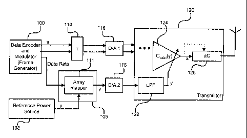
As illustrated in Figure 1, a frame generator 100, such as a data encoder and
modulator, generates a signal, s, which is transmitted to an amplifier 124 in
transmitter
120. In series with AGC amplifier 124 is the amplifier stage manifesting gain
incremental
AG 126. Amplifier 124 is controlled by amplifier controller 105 to mitigate
the
nonlinearities of gain incremental AG 126.
The transmitted signal is gain adjusted by the AGC amplifier 124 in accordance
with a control signal y, and then provided to the amplifying stage that
manifests the signal
dependent gain variation AG 126, whose value is dependent on the input signal
level, input
signal data rate, and input signal format. For simplicity, the following
description ignores
sources of gain variation such as temperature, frequency, and battery voltage
related gain
variations. Instead, the focus is on AG itself and an aspect that is tightly
coupled with AG:
the AGC control characteristic, which is the gain of the AGC amplifier 124 in
dB as a
function of the control voltage of the voltage-controlled AGC amplifier 124.
As used
herein and throughout the specification, a "reference signal" or a "reference
data rate and
signal format" means a data rate and signal format, often arbitrarily chosen,
that is used for
calibration procedures.
CA 02504687 2007-07-20
Frame generator 100 generates the encoded and modulated signal frames to be
transmitted at one of a plurality of supported data rates. The data rate may
vary over time.
The total power of the output signal, s, containing the encoded and modulated
signal
frames, produced by the frame generator is normalized to the same mean power
level for
all data rates, and the relative power of the individual code channels are
also accurately
regulated by digital means to the desired values. A data rate and signal
format indicator
signal, r, is also generated simultaneously by the frame generator. In one
embodiment, a
delay block "i" 114 is employed to ensure time alignment of signal s and the
amplifier
controller signal y. One skilled in the art will appreciate that the delay
block "i" 114 may
not physically exist as a delay unit in an implementation, so long as the
alignment of
signal s and the corresponding amplifier control signal is maintained. The
transmitted
signal s, after delay alignment and digital to analog conversion at D/Al 116,
is fed to the
transmitter 120. Signal s is gain adjusted by AGC amplifier 124 and is
affected by signal
dependent gain, AG 126, before it is transmitted.
On a second data path, data rate and signal format indicator r, is provided by
frame
generator 100 and is received by a first mapper 106 in amplifier controller
105. First
mapper 106 contains a mapping from the data rate and signal format r to a gain
adjustment
amount d(r) that is generated through a calibration process to ensure that the
nonlinearities
of signal dependent gain AG 126, are properly compensated for. The process of
calibration
is discussed in greater detail below. This adjustment d(r) is a value in dB or
proportional to
dB by a scaling factor. For a chosen reference data rate, denoted as r,ef, the
value d(rref) is
set as 0 dB. A reference power source 108 produces the desired reference power
level p
that is expected at the antenna in dBm (or in a unit proportional to dBm by
the same
scaling factor as used in d(r), if any). One skilled in the art will
appreciate that the system
can be simplified by ensuring that the scaling factor used in p for the power
expected at
the antenna, is the same scaling factor used in d(r) for the gain offset. In
cdma2000 mobile
devices, reference power level p is derived from both the open loop and closed-
loop power
control system. This derivation of reference power level p is well understood
in the art.
Both d(r) and p are provided to a second mapper 110, preferably after being
combined by
an adder 112. With proper calibration of first mapper 106, the value resulting
from the
additive combination of d(r) and p is related to the desired degree of
amplification for
6
CA 02504687 2007-07-20
signal s. This value is provided to the second mapper 110 to map to an
amplifier control
signal y. The mapping table values in the second mapper 110 are determined by
calibration procedures that reflect implementation specific information about
AGC
amplifier 124, signal dependent gain variation 126 and other elements of
transmitter 120.
The amplifier control signal y is provided to a control input of amplifier
124, and is
preferably aligned with signal s in time at the output of AGC amplifier 124.
Signal s and amplifier control signal y are preferably converted from digital
signals
to analog representations of the digital signals by digital-to-analog
converters 116 and 118,
respectively. The analog representation of amplifier control y may also be low-
pass-
filtered by LPF 122, to smooth the control of amplifier 124. AGC amplifier 124
then
amplifies the analog representation of signal s in accordance with smoothed
amplifier
control signal y', the analog representation of y, or a filtered version
thereof. The result of
the amplification is that signal s is amplified in a manner that compensates
for the signal
dependent gain AG 126.
The method to calibrate the first mapper 106 and the second mapper 110 mapping
table values will now be described. Using a reference signal generated by the
frame
generator 100 with a reference data rate and signal format, the second mapper
110 output
value y is calibrated by the system of the presently illustrated embodiment as
follows. For
a reference data rate and signal format rref the value d(rref) is defined as 0
dB, for each
given value p, the second mapper 110 adjusts output value y corresponding to p
so that the
transmitted reference power measured at the antenna is the expected value p.
Note that the
manner in which the value y is determined already compensates both the
nonlinear
relationships in the transmitter, i.e., the gain in dB of amplifier 124 as a
function of the
value of the amplifier control signal y, and variation in the AG 126 as a
function of the
input signal level, where the input signal for calibration is the selected
reference data rate
and signal format. For example, choosing RC 1 in IS-2000-2 as the reference
signal, the
reference power is the total gated on transmitted power. The calibrated value
y stored in
the second mapper results in the expected total transmitted power p at antenna
for any
value of p generated by the reference power source 108.
The output of the first mapper 106, d(r), is preferably calibrated as follows:
for
each data rate and signal format r that the mobile device supports, and for a
pre-selected
7
CA 02504687 2007-07-20
value of p, the value d(r) is adjusted so that the transmitted output
reference power
measured at the antenna for data rate r is p. Note the manner in which the
value d(r) is
determined results in d(r) being composed of two parts. The first part
accounts for the
difference in dB in total transmitted power between r and rref, given the same
reference
power, where r and rref are the current and the reference data rates and
signal formats,
respectively. This part usually can be pre-calculated according to standard.
The second
part compensates for the gain difference in AG 126, between data rates and
signal formats
r and rief, which is caused by the signal distribution change between r and
rref. This second
part usually cannot be pre-calculated and has to be calibrated, if
significant. Whenever the
data rate and signal format changes, the appropriate gain adjustment d(r) is
applied at the
same time because the two paths are delay aligned, as has been described
above. In the
above calibration, it is assumed that the gain variation in dB caused by data
rate and signal
format change is nearly independent of that caused by signal level change,
which is true in
a large range of operation of interest.
In instances where signal level and signal distribution caused gain variations
are
dependent, an alternative embodiment as shown in Figure 2 can be used to
compensate for
the dependent gain variations. Referring to Fig. 2, the first mapper 106 is an
array of
mappers. The data rate and signal format indicator r is used to select a
member mapper
within the array. Each member mapper of the array selected in accordance with
r receives
the desired reference power level p from reference power source 108 and maps
it to a
corresponding output value d(r, p) in accordance with the values of p and r.
Following the
mapping of p and r to d(r,p), and after d(r,p) is additively combined with p
from reference
power source 108 at an adder 112, the combined signal is provided to second
mapper 110,
which maps the sum of d(r,p) and p to an amplifier control signal y. Other
aspects of this
embodiment preferably remain the same as in the embodiment shown in Fig. 1.
The method to calibrate the second mapper 110 also remains the same as
described
hereinabove for the embodiment of Figure 1. In this instance, the adjustment
amount
d(r, p) stored in the mapper 106 is calibrated for each data rate and signal
format r
respectively so that, for each value of the desired reference power level p
input to the first
mapper 106, the required reference power p is achieved at the antenna.
8
CA 02504687 2007-07-20
Alternatively in a further embodiment, as shown in Figure 3, the first and
second
mappers, 106 and 110, and the adder 112 are removed and replaced by an array
mapper
111 with two inputs. The first input is the data rate and signal format
indicator r provided
by the frame generator 100; the second input is the desired reference power p
provided by
the reference power source 108. The input r selects a member mapper in the
array mapper
111 that maps the input p to an output of amplifier control signal y. Other
aspects remain
the same as in the embodiments in Fig. 1 or Fig. 2. Each of the member mapper
contains a
mapping table that is calibrated for the corresponding r to get correct
reference power
value p at the antenna for any value p provided by the reference power source
108.
Figure 4 illustrates a method according to an embodiment of the present
invention.
In step 200 the data rate and signal format of the generated signal s are
received. The
desired degree of amplification is determined in accordance with the data rate
and signal
format of the received signal, the reference power level and pre-calibrated
values
determined in accordance with the nonlinear characteristics of the amplifiers
in step 202.
This desired degree of amplification is subsequently mapped to an amplifier
control signal
value in step 203. The mapping of the desired degree of amplification to the
amplifier
control signal value is preferably performed in accordance with pre-calibrated
values
reflecting characteristics of the amplifiers and transmitter system. In step
204, an amplifier
control signal is generated in accordance with the mapping of step 203.
Figure 5 illustrates another method according to an embodiment of the present
invention. As before, in step 200 the data rate and signal format of the
generated signal are
received. Step 202, the determination of the desired degree of amplification,
is achieved
by first selecting a member mapping table in accordance with the determined
data rate and
signal format as shown in step 208. And then, at step 209, receive the desired
reference
power level and map it to a pre-calibrated gain adjustment value that reflects
the non-
linear signal dependent gain characteristics of the amplifiers corresponding
to the
determined data rate and signal format. In step 210 the degree of
amplification is
determined in accordance with both the pre-calibrated gain adjustment value
and the
reference power level. In step 203, the determined desired degree of
amplification is
mapped to an amplifier control signal value. In step 204, an amplifier control
signal is
generated in accordance with the mapping of step 203.
9
CA 02504687 2007-07-20
For the embodiment employing array mapper 111, there is the exemplary method
illustrated in Figure 6. In step 200, the data rate and signal format of the
generated signal
are received. Along with the desired reference power level, these values are
used, in step
202a, to select one of an array of maps which account for the nonlinearities
of the
amplifier, much as the degree of amplification was previously determined using
the same
inputs. The selected mapping is used in step 203a to map the reference power
level to an
amplifier control signal value. The amplifier control signal value is used in
step 204 to
generate the amplifier control signal.
The above-described embodiments of the present invention are intended to be
examples only. Alterations, modifications and variations may be effected to
the particular
embodiments by those of skill in the art without departing from the scope of
the invention,
which is defined solely by the claims appended hereto.