Note: Descriptions are shown in the official language in which they were submitted.
CA 02505017 2005-05-04
WO 2004/042321 PCT/F12003/000814
1
Synchronous optical measurement and inspection method and means
TECHNICAL FIELD OF THE INVENTION
The invention relates to a method and means for finding defects in materials.
In
particular, the invention relates to a method for finding holes, spots, edge
defects and other related defects and measuring characteristics of sheets of
industrial material.
Even more particularly the invention is related to industrial optical systems
used for inspecting and measuring products manufactured in a continuous
fashion, such as steel, aluminium, papers, foils and plastics.
BACKGROUND OF THE INVENTION
There are numerous optical methods for finding optically visible defects, such
as holes or spots in industrial material sheets. Manufacturers of such strip
or
web materials use optical inspection and measurement systems e.g. for
controlling the manufacturing process of the materials in order to improve
yield
in terms of improved quality, decreased waste and machine down time on the
manufacturing line.
The optical measurement systems referred here typically operate online i.e.
simultaneously with the product manufacturing and are non-contacting.
Detection of such quality defects as pinholes, holes, spots, scratches,
streaks,
cracks, cuts, tears or edge defects are important applications where
aforementioned optical inspection and measurement systems may be used.
Defects or material properties of other kinds may also be measured with the
described systems. Web or strip sheet width, length or edge position
measurements, are other examples of the possible uses of these systems.
One of the methods in accordance with prior art utilises CCD (Charge Coupled
Device) cameras. The operation of a CCD camera cell can be divided into two
distinctive periods: the integration period and the readout period. During the
integration period the cell is active in terms of light intensity measurement
and
CA 02505017 2005-05-04
WO 2004/042321 PCT/F12003/000814
2
during the readout period it is not. In a typical CCD camera system each CCD
camera cell records the integrated light intensity falling upon it during a
certain
integration period. The resulting integrated electrical charge is stored in
each
CCD cell until the cell is read out. Typically the total electric charge
generated
by the photons is stored in a capacitor in each pixel. As a photon hits a
pixel, a
small amount of charge is added to the capacitor. This process is called the
integration period of the device.
The integration period continues until a certain time has elapsed, and after
the
completion of the integration, readout period starts. In the readout phase the
charge proportional to the incident photon number is observed and recorded,
and thus incident photon number can be deduced with certain accuracy. After
the readout is complete, the CCD is flushed from the stored charges and a new
integration period starts.
For example the ULMA product range from ABB Corporation has utilised
CCD cameras in web inspection, please see "ULMA Nti tuote data" product
publications for reference from ABB. Earlier ULMA products have also
utilized phototransistors generating photocurrent.
Figure 1 shows a flow diagram explaining the prior art. In phase 101 a
material
sheet is stationary or is traversed between and/or in front of one or more
optical
light sources and light detectors. In phase 111 a light source, or several
emit
light beams and shine the beams on a material sheet. In phase 121 light beam
targeted towards the material interacts with the material sheet to be
inspected or
measured.
In phase 131 light is detected at a light detector or light detectors. The
light
detector or light detectors convert incident light into photocurrent signals
in
phase 141. In phase 151 the photocurrent signal is processed and manipulated
to determine characteristics of the material. Prior art solutions of this type
are
found for example from GB 2181834 and GB 2087544 which are cited as
reference.
Photo multiplier tubes (PMTs) are also used for inspection and measurement of
defects in materials manufactured in a continuous fashion. PMTs are most
typically used for detection of pinholes in materials. Holes or pinholes in a
material sheet may be detected by using a UV (Ultraviolet) light source or a
CA 02505017 2005-05-04
WO 2004/042321 PCT/F12003/000814
3
scanning, laser light source on one side of a material and one or several PMTs
on the other side. In this case the PMT or PMTs are used to detect the UV or
laser light transmitted through the hole while the material traverses the
measurement system.
There are several inherent disadvantages in the prior art. The prior art
method
of figure 1 is prone to ambient light, both optical and electrical noise and
the
level on signal strength is typically also a problem.
The CCD devices are integrating and imaging devices; there are strict limits
on
the speed of detection. If the material is traversed faster, the CCD equipment
may be unable to photograph the whole surface area of the sheets, due to the
latency in integration and image readout. The integration method CCD cameras
are based upon is incremental, not continuous, and therefore undesirably slow
and unreliable. The integration periods of CCDs are also typically quite long
for the purposes of dynamical defect detection.
CCD systems also typically operate with visible wavelengths, and ambient light
is therefore a problem. A significant disadvantage of the prior art is that
either
the system has to be covered from ambient light, or it must bear the errors
caused by ambient light. Optical filtering is typically inefficient, as the
measurements are done at the same wavelengths as ambient light.
CCD camera systems are imaging systems that produce photograph like, digital
images of the material to be inspected or measured. All the image information
produced by the CCD camera must typically first be stored in specialized
image processing electronics or in computer memory and then transferred
and/or analysed in a computer system to distinguish useful measurement
information from all unnecessary information. The CCD camera itself cannot
discriminate and select inspection or measurement data useful for the user of
the system. Especially in large industrial inspection and measurement systems,
extensive data storage, transfer and computing capacity is therefore required.
In
many factories or industrial facilities computer systems of this scale are
very
expensive and tedious to arrange.
PMTs are mechanically vulnerable and measurement systems based on PMTs
are poor in terms of shock or vibration resistance. UV light based PMT systems
are also notoriously unstable, as the UV-source lifetime is typically only 1-2
CA 02505017 2005-05-04
WO 2004/042321 PCT/F12003/000814
4
months. Despite basically different wavelengths of the system light source and
ambient light, PMTs are also sensitive to ambient wavelengths and ambient
light remains a problem. In the edge area of the material under inspection,
separate, mechanical edge following light shields must be used along the sides
of the material, to prevent the PMTs located at the edge of the material from
becoming saturated and therefore non-operational. The mechanical edge
following shields are unreliable since these light shields need to be
mechanically moved in demanding industrial environments with possible
harmful interference with the material to be inspected or measured.
Any moving parts or parts mechanically interacting with the material to be
inspected or measured are undesirable because of reliability reasons. For
example, the edge followers are prone to cause measurement errors as they are
subject to mechanical shear, strain and stress, and may typically move to
destroy the calibrations of the delicate measurement system. Design of PMT
based UV inspection systems for wide material sheets is quite unpractical due
to the extensive demands set on mechanical engineering and high cost.
For clarification the opportunity is taken to define the following terms:
"Light receiver" and "light detector" are used in this application
interchangeably. "Light detector" refers with emphasis to the semiconductor
part of the light receiving detector and its associated optical, mechanical
and
electronic parts. "Light receiver" refers foremost to the entire optical,
mechanical and electrical arrangement for receiving the light and comprises at
least one light detector.
"Synchronisation signal" is a signal that is used to synchronise an emitter
and a
receiver with respect to waveform, phase and/or frequency of the signal.
SUMMARY OF THE INVENTION
The object of the invention is to relieve and remove some of the
aforementioned disadvantages. The invention exhibits an optical inspection and
measurement method and means which is resistant to intense ambient light and
noise and is capable of inspecting sheets of material continuously, without
incremental integration, and without losing information.
CA 02505017 2005-05-04
WO 2004/042321 PCT/F12003/000814
It is a further object of the invention to produce only data required for the
inspection or measurement, at data production rates that are relatively low
compared to prior art. An even further embodiment of the invention is to
measure a wide diversity of different properties from the material sheet with
a
5 single optical inspection and measurement method and means.
Various embodiments of the invention may be constructed of solid-state
components and are therefore mechanically more reliable and shock and
vibration resistant compared to the prior art. One object of the invention is
not
to require use of mechanically moving system parts and measure the samples in
a non-contacting fashion.
Most of the aforementioned advantages of the invention are achieved with an
inspection and measurement method where the basic measurement and
inspection signal is the photocurrent generated in a light sensitive
electrical
component (photoelectric device). This photocurrent is used continuously and
directly as the basic measurement and inspection signal. The photocurrent
signal appears in the vicinity of a carrier frequency generated in the
measurement system for the purpose of synchronised light emission and light
detection. The photocurrent is modulated by light interactions with the
material
to be inspected or measured, and further demodulated in the receiver part to
remove the effects of ambient interference, noise and the carrier frequency.
Several emitters send beams to a single receiver, and the emitters are
synchronised with the detector. The different beams typically have different
carrier frequencies, and measure different properties from the sheet.
In one particular embodiment of the invented method, the system comprises at
least one LED (Light Emitting Diode) based light source, at least one
photodiode based light detector, at least one waveform generator device
generating an AC sinewave or square wave control signal, the carrier signal
for
synchronisation of at least one LED based light source and at least one
photodiode based light detector. In this embodiment several phases, processes
and arrangements take place to accrue inventive advantages:
- a sheet of material to be inspected or measured is traversed between and/or
in
front of at least one light source and at least one light detector,
CA 02505017 2005-05-04
WO 2004/042321 PCT/F12003/000814
6
- at least one waveform generator generates an electrical signal (carrier) of
a
repeating AC waveform at a given frequency for synchronised control and
operation of the light source and the light detector,
- at least one light source emits light, intensity of which follows a carrier
waveform of a waveform generator,
- light emitted by at least one light source is targeted on the material sheet
or a
part of it and/or the edge of the sheet to be inspected or measured,
- at least one beam of light is stopped by the sheet, reflects from the sheet,
passes partly through the sheet, passes through apertures or holes or defects
in
the sheet, passes partly by the sheet or otherwise interacts with the material
sheet to be inspected or measured in a manner which results in amplitude
modulation (AM) of the intensity of the light beam by the material,
- at least one light detector detects and measures an amplitude modulated
light
beam signal after it has interacted with the material sheet to be inspected or
measured,
- at least one light detector converts an amplitude modulated light signal it
has
received into continuous electrical photocurrent,
- at least one light detector or following analog signal processing
electronics of
the system, utilize at least current-to-voltage conversion and synchronised
detection or demodulation in the further signal processing of the photocurrent
signal for improving the quality and signal-to-noise ratio of the inspection
or
measurement signals of the system,
- analog signal processing part of the system produces one voltage signal
(demodulated signal) for each light detector,
- the momentary absolute value of the demodulated signal of a light detector
is
proportional to the amplitude of the modulating effect of the interaction
between the light signal and the material sheet to be inspected of measured,
- demodulated signal amplitude and/or a rapid change in the demodulated
signal is observed, recorded and analysed by the inspection or measurement
system to measure certain properties of the material sheet, such as sheet
width,
sheet length or edge position of the sheet, or to locate defects or
imperfections
CA 02505017 2005-05-04
WO 2004/042321 PCT/F12003/000814
7
in the sheet, such as pinholes, holes, spots, scratches, streaks, cracks,
cuts, tears
or edge defects in the material,
- more than one beam from more than one emitter are synchronised with one
detector, and different beams measure different properties.
The aforementioned is also considered at the moment to present the best mode
of the invention. The best mode of the invention is especially applicable for
the
purpose of detecting the three-dimensional structure of the defects in the
material sheet with multiple light beams synchronised to the same detector.
An optical measurement and inspection method in accordance with the
invention comprises at least two light emitters, at least one light receiver,
at
least one signal generator connected to at least one light emitter and at
least one
light receiver and means for converting the received light to electrical
current,
and is characterised in that,
- a sheet of material lies or traverses between and/or in front of at least
two
light emitters and at least one light receiver,
- at least one signal generator controls at least one light emitter and at
least one
light receiver by sending them a synchronisation signal and thereby
synchronises the emission and detection of light rays,
- at least one signal generator drives at least two light emitters with
different
carrier frequencies, waveforms and/or phases, and at least one light receiver
with both of these frequencies waveforms, and/or phases,
- at least two light emitters emit at least two rays of light,
- at least two rays are incident on the stationary or traversing sheet,
- at least two grazing, transparent and/or reflected rays of light from the
sheet
or directly from the light emitters are detected by the same light receiver,
- at least two rays of light are converted to photocurrent,
- the processed photocurrent and/or changes in the processed photocurrent are
diagnosed and observed to find defects and/or determine characteristics of the
said sheet of material.
CA 02505017 2009-05-08
8
An optical measurement and inspection arrangement in accordance with the
invention comprises at least two light emitters, at least one light receiver,
at
least one signal generator connected to at least one light emitter and at
least one
light receiver and means for converting the received light to electrical
current
and is characterised in that,
- a sheet of material is arranged between and/or in front of at least two
light
emitters and at least one light receiver,
- at least two light emitters are arranged to emit at least two rays of light
incident on at least one sheet,
- at least two grazing, transparent and/or reflected rays of light are
arranged to
be detected by the same light receiver,
- at least one ray of light is arranged to be converted to photocurrent by at
least
one photoelectric device,
- at least one signal generator is arranged to control at least one light
emitters
and at least one light receiver by sending them a synchronisation signal and
thereby synchronises the emission and detection of rays,
- at least one signal generator is arranged to drive at least two light
emitters
with different carrier frequencies, waveforms and/or phases, and at least one
light receiver with both of these frequencies, waveforms and/or phases,
- the photocurrent and/or changes in photocurrent are arranged to be diagnosed
and observed to find defects and/or determine characteristics of the said
sheet
of material.
In accordance with a first aspect of the present invention, there is provided
an
optical measurement and inspection method comprising:
providing at least two light emitters,
providing at least one light receiver,
providing at least one signal generator connected to at least one of the
light emitters and the at least one light receiver, and
CA 02505017 2009-05-08
8a
providing means for converting the received light to electrical current,
wherein
providing a sheet of material that lies or traverses between and/or in front
of the at least two light emitters and the at least one light receiver,
controlling, with the at least one signal generator, at least one of the light
emitters and the at least one light receiver by sending them an electronic
synchronisation signal and thereby synchronises emission and detection of
light
rays,
fixing a common carrier waveform AC voltage signal in frequency, and a
symmetrical 50% duty cycle wave signal is processed from the common carrier
AC voltage waveform signal and the common carrier waveform AC voltage
signal and the 50% duty cycle wave signal carry equal frequency and phase in
terms of zero-crossings,
driving, with the at least one signal generator, the at least two light
emitters with different carrier frequencies, waveforms and/or phases, and the
at
least one light receiver with both of these frequencies, waveforms and/or
phases,
emitting, with the at least two light emitters, at least two rays of light,
the at least two rays of light being incident on the stationary or traversing
sheet,
detecting by the same light receiver at least two rays of light grazing the
sheet, transparent to the sheet, reflected from the sheet or directly from the
light
emitters,
an intensity of at least one said emitted ray of light follows at least one of
the carrier waveform signals and at least one said detected light ray is
demodulated from the carrier waveform signal using the electronic
synchronisation signal,
converting at least two of the rays of light to photocurrent, and rectifying
photocurrent signal with the symmetrical wave signal, processed from the
common carrier waveform signal,
CA 02505017 2009-05-08
8b
removing at least one DC component from the photocurrent signal, and
diagnosing and observing the processed photocurrent and/or changes in
the processed photocurrent to find defects and/or determine characteristics of
the
said sheet of material,
wherein at least one said carrier waveform signal is a sine wave, cosine
wave, or a square wave signal.
In accordance with a second aspect of the present invention, there is provided
an
optical measurement and inspection arrangement, comprising:
at least two light emitters,
at least one light receiver,
at least one signal generator connected to at least one of the light emitters
and at least one of the light receivers, and
means for converting the received light to electrical current, wherein
a sheet of material is arranged between and/or in front of the at least two
light emitters and the at least one light receiver,
the at least two light emitters are arranged to emit at least two rays of
light
incident on at least one sheet,
at least two rays of light grazing the sheet, transparent to the sheet or
reflected from the sheet are arranged to be detected by the same at least one
light
receiver,
at least one ray of light is arranged to be converted to photocurrent by at
least one photoelectric device,
the at least one signal generator is arranged to control at least one of the
light emitters and at least one of the light receivers by sending them an
electronic
synchronisation signal and thereby synchronises the emission and detection of
rays,
CA 02505017 2009-05-08
8c
a common carrier waveform AC voltage signal is fixed in frequency, and a
symmetrical 50% duty cycle wave signal is processed from the common carrier
AC voltage waveform signal and the common carrier waveform AC voltage
signal and the 50% duty cycle wave signal carry equal frequency and phase in
terms of zero-crossings,
the at least one signal generator is arranged to drive the at least two light
emitters with different carrier frequencies, waveforms and/or phases, and the
at
least one light receiver with both of these frequencies, waveforms and/or
phases,
an intensity of at least one said emitter ray of light is arranged to follow
at
least one of the carrier waveform signals and at least one received light ray
is
arranged to be demodulated from the carrier waveform signal using the
electronic
synchronisation signal,
the symmetrical wave signal, processed from the common carrier
waveform signal, is configured for rectifying photocurrent signal,
at least one DC component is removed from the photocurrent signal, and
the photocurrent and/or changes in photocurrent are arranged to be
diagnosed and observed to find defects and/or determine characteristics of the
said sheet of material, wherein at least one of said carrier waveform signal
is a
sine wave, cosine wave, or a square wave signal.
BRIEF DESCRIPTION OF THE DRAWINGS
Next the invention is described in greater detail with reference to exemplary
embodiments in accordance with the accompanying figures, in which:
Figure 1 shows a method 10 in accordance with the prior art as a flow diagram
on
a general level.
CA 02505017 2005-05-04
WO 2004/042321 PCT/F12003/000814
9
Figure 2 shows an inspection and measurement method 20 based on
synchronised optical detection in accordance with the invention as a flow
diagram.
Figure 3 shows a detailed exemplary embodiment 30 of the invented inspection
and measurement method 30 based on synchronised optical detection in
accordance with the invention.
Figure 4 shows a front view of an arrangement 40 for measurement and/or
defect inspection of a material sheet in accordance with the invention.
Figure 5 shows a more detailed front view of an arrangement 50 and an optical
ray diagram of an arrangement for measurement and/or defect inspection in
accordance with the invention.
Figure 6 shows an arrangement 60 and an optical ray diagram of an
arrangement for measurement and/or defect inspection in accordance with the
invention from a side view.
Figure 7 shows a more detailed arrangement 70 and an optical ray diagram of
an arrangement for measurements and defect inspection in accordance with the
invention from a side view.
Figure 8 shows an exemplary, functional block diagram for a fault detection
circuit and method 80 in accordance with the invention.
Some embodiments of the invention are described in the dependent claims.
DETAILED DESCRIPTION
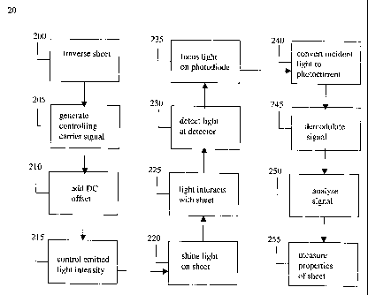
Figure 2 displays an inspection and measurement method, where synchronous
detection in accordance with the invention is used. In phase 200 a material
sheet to be inspected or measured lies or traverses between and/or in front of
at
least one light source and at least one light detector. In phase 205 a
controlling,
constant frequency carrier signal is generated in a waveform generating device
for the purpose of synchronisation of emission and detection of light beams in
the measurement system. The carrier may have an AC sine wave, square wave
or other waveform. The carrier signal is delivered to at least one light
source
CA 02505017 2005-05-04
WO 2004/042321 PCT/F12003/000814
and at least one light detector for the synchronised control of these system
parts. In phase 210 a DC offset may be added to a carrier signal before using
it
for light source control to guarantee that some light intensity is emitted
also at
AC control signal values corresponding to lowest emitted light intensity. In
5 some embodiments of the invention DC offset may not be required and phase
210 is therefore optional.
In some embodiments of the invention several waveform generating devices
may be used to generate several waveforms and/or several frequencies in order
to build measurement or inspection systems where a light detector may
10 simultaneously detect, distinguish and separate light signals originating
from
different light sources operating at different waveforms and/or waveform
frequencies. Several waveform generating devices and waveforms and/or
frequencies may also be used for the purpose of isolating two, at least partly
independent but closely spaced inspection or measurement systems from each
other in terms of light signal disturbance from one system to another. Several
emitters and beams may be focused to a particular detector that is
synchronised
with these emitters. The different beams and emitters may have different
carrier
frequencies and they may measure different properties from the material sheet.
For example, a few beams may depict the three dimensional structure of a
defect by measuring its area, height, width, depth, diameter, circumference,
reflectivity or the like, properties from which the three dimensional
structure
may be deduced.
The intensity of a light beam emitted by a light source is controlled in phase
215 by the carrier signal which may have been DC shifted in optional phase
210. The carrier signal is used for controlling at least one light source
and/or at
least one light detector. In phase 220 the carrier controlled light beam from
the
light source is shone on the material. The intensity of the light beam follows
the
waveform of the carrier signal. In phase 225 light beam or beams are incident
on the material sheet to be inspected or measured, and light is absorbed and
stopped by the sheet, reflects from the sheet, passes partly through the
sheet,
passes through apertures or defects in the sheet, passes partly by the sheet
or
otherwise interacts with the sheet. Typically several of the aforementioned or
other interactions happen simultaneously or sequentially. Thus the sheet
modulates the amplitude of the light signal initially appearing at the carrier
frequency and following carrier waveform. In phase 230 interacted and
CA 02505017 2005-05-04
WO 2004/042321 PCT/F12003/000814
11
modulated light signal is detected at a light detector. Depending on
measurement geometry, inspection or measurement system structure and
interactions with the material sheet, a varying amount of light originating
from
one or more light sources is received by each light receiver in phase 230. In
phase 235, a light receiver collimates or focuses the light on a photodiode,
APD
(Avalanche Photodiode), any other semiconductor based photoelectric, light
sensitive component or any other photoelectric device designed for the purpose
of detecting light signals. The collimation and/or focusing may be implemented
by using light pipes and/or lenses or other optical components. In phase 240
the
photoelectric device converts the incident light into photocurrent. The
photocurrent is then manipulated and demodulated or in other terms,
synchronously detected in phase 245 in order to remove carrier frequency from
the signal and to recover the lower frequency, modulated signal of interest.
The
resulting demodulated signal is proportional to the amplitude of the
modulating
effect of one or several interactions between the initial, carrier frequency
light
signal and the material sheet. In phase 250 the demodulated signal is fed into
analysis electronics and software for the purpose identifying signals and
signal
events of interest and the signal is analysed. In phase 255 the absolute value
and/or rapid changes in the demodulated signal are observed, recorded and
analysed. Analysis results are exploited to measure selected properties of the
material sheet, and/or to detect defects or imperfections in the material
sheet.
It is clear that within the scope of the invention one or several light
sources and
one or several light detectors and receivers may be in any line of sight
positions
with respect to the inspected sheet. Transparent and reflected beams of light
as
well as light beams interacting by other means may be used in said
measurement or inspection systems. In some embodiments phases 200, 205,
210, 215, 220, 225, 230, 235, 240, 245, 250, 255 and 260 may take different
permutations in accordance with the invention.
It is also clear that several light beams may have different carrier waveform
frequencies in different methods. The different frequencies are useful in
distinguishing signals from various emitters at the receiver end. It is
therefore
possible to route several beams to a particular receiver and use the same
receiver in analysing measurements from different optical paths. This allows
complex designs of three dimensional detection systems, applicable for
detecting defect structures in three dimensions.
CA 02505017 2005-05-04
WO 2004/042321 PCT/F12003/000814
12
Figure 3 displays one particular and typical embodiment of the invention at a
more detailed level. In phase 300 a material sheet to be inspected or measured
traverses between and/or in front of one or more light sources and light
receivers. In phase 305 a controlling, constant frequency carrier signal of AC
sine wave waveform is generated in an electronic signal generator for the
purpose of synchronisation of one or several light sources and one or several
light receivers in the measurement system. The AC sine wave carrier signal is
delivered to at least one light source and at least one light receiver for
synchronised operation of the measurement system. In phase 310 a DC offset is
added to the AC sine wave carrier signal to guarantee the linearity of at
least
one emitter.
The intensity of a light beam emitted by a light source is controlled in phase
315 by the DC shifted, sine wave carrier signal. The DC shifted carrier signal
is
used for controlling one or several light sources. Light sources are LED
based,
solid state light sources. The DC shifted AC sine wave carrier is directly
converted into forward currents signals of individual LEDs in order to
implement emitted light intensity signal following the sine wave waveform of
the carrier. The light signal intensity therefore consists of a DC component
and
an AC sine wave component. A square wave signal derived from the AC sine
wave carrier signal is used for controlling one or several light detectors. In
phase 320 an AC sine wave carrier controlled light beam from a light source is
shone on the material. In phase 325 light beam or beams are incident on the
material sheet to be inspected measured, and light is absorbed and stopped by
the sheet, reflects from the sheet, passes partly through the sheet, passes
through apertures or defects in the sheet, passes partly by the sheet or
otherwise
interacts with the sheet. Thus the material sheet modulates the DC shifted, AC
sine wave amplitude of the light signal initially appearing at the sine wave
carrier frequency. In phase 330 interacted and modulated light signal is
detected at a photodiode based light detector. Light pipes and lenses are used
for collimating and focusing light to the active area of a silicon photodiode
in
phase 335.
In phase 340 the silicon photodiode absorbs the incident light photons and
light
is converted into photocurrent. A transimpedance amplifier may be used in
phase 340 to convert the signal current produced by the photodiode into signal
voltage and amplify it.
CA 02505017 2005-05-04
WO 2004/042321 PCT/F12003/000814
13
In phase 345 the control signal (carrier) received by the signal processing
electronics from the waveform generator is utilized to perform first step of
synchronized detection, rectification of the signal. In this typical
embodiment
the rectified signal is further low-pass filtered in phase 345 to finalize
synchronized detection. The filter circuit used in this embodiment is
typically a
Bessel filter but may also be a Gaussian-, Chebyshev-, Butterworth- or an RC -
filter. Phases 340 and 345 together perform the function of demodulation or
synchronised detection in some embodiments.
Manipulation and synchronised detection of the photocurrent signal, which
may also be called demodulation of the photocurrent signal, results in that
low
frequency signal components carried by the carrier frequency are therefore
present in the photocurrent signal in the vicinity of the fixed frequency of
the
waveform generator (the carrier frequency) are effectively amplified and
detected whereas signals, noise and disturbance at other frequencies,
especially
at low frequencies are effectively attenuated. In a typical embodiment of the
invention, a fixed frequency AC sine wave voltage is generated by the
waveform generator to act as the carrier and a symmetrical, 50% duty cycle,
square wave signal, processed from the sine wave signal and carrying equal
frequency and phase in term of zero-crossings, is used for rectifying the
manipulated photocurrent signal in phases 340, 345 after first removing any
DC components of the signal. In this typical embodiment rectified signal is
low-pass filtered to finalize synchronised detection, and demodulated voltage
signal is produced in phase 350.
In a typical embodiment the absolute value of the demodulated signal is
measured and recorded in phase 360 by using an ADC electronics component.
In phase 365 the AC voltage produced is further fed into the signal processing
electronics, which performs processing on the basic AC voltage signal. The
signal processing electronics may be part of the light detector itself or a
part of
system level electronics of the inspection or measurement system. The purpose
of signal processing is to remove and reduce noise and interference still
present
in the signal due to e.g. ambient light, other light sources and/or noise
present
in the signal electronics of the system in general. Synchronised detection
heavily depresses the effect of ambient light.
CA 02505017 2005-05-04
WO 2004/042321 PCT/F12003/000814
14
The purpose of the signal processing is also to remove carrier frequency from
the signal and to recover the lower frequency, modulating signal of interest
phases (345, 350). This step exhibits the key benefits of synchronous
detection
by removing and reducing noise and interference still present in the signal
due
to e.g. ambient light, other light sources or system electronics. The
resulting
signal, demodulated signal is proportional to the amplitude of the modulating
effect of one or several interactions between the initial carrier frequency
light
signal and the material sheet.
It is clear that other waveforms than the aforementioned AC sine wave voltage
may be generated by the waveform generator within the range of the invention
and other means, including linear demodulation by using a linear signal
multiplication instead of square-wave signal rectifying may be used for
demodulation or synchronized detection of the photocurrent signal. Quite
clearly, the signal that drives the emitter may have a different waveform to
the
one that synchronises the emitter and a receiver. In one preferable
embodiment,
sine wave signal is used to drive the emitters, and a square wave signal
derived
thereof is used to synchronise at least one emitter and receiver.
In some embodiments in phases 350, 360 and 365 the signal output of the
signal processing (demodulated signal) is further fed into and processed by
system level electronics which may include dedicated electronics to track
changes in the demodulated signal which are not normal for the material to be
inspected or measured. In a typical embodiment demodulated signal may be
further filtered by a low pass filter in one signal path and a comparator
circuit
may be used to track faster changes of the demodulated signal by subtracting
low-pass filtered demodulated signal and the original demodulated signal from
each other. In this exemplary embodiment a certain signal difference threshold
may be used in the comparator to produce a digital defect pulse when e.g. a
hole or a spot is measured by the system.
In some embodiments the absolute value of the demodulated signal may also be
observed, recorded and analysed in phases 360, 365 to deduce data intended for
locating defects or imperfections in the material to be inspected or measured
or
especially if certain properties of the material, such as sheet width, sheet
length
or edge position of the sheet are to be measured.
CA 02505017 2005-05-04
WO 2004/042321 PCT/F12003/000814
The digitised signal values produced by the ADC are analysed in phase 365, in
the system level digital signal processing electronics and software. The
analysis
typically produces data depicting the properties of the sheet in phase 370.
This
data can be made visible to the user of the inspection or the measurement
5 system through a computer monitor but the invented optical detection system
may also be integrated with any other production systems or factory automation
systems to trigger automatic actions in the production of a materials
manufactured in a continuous fashion, such as steel, aluminium, papers, foils
and plastics. Likewise the data produced may be accessible to production
10 management software, enterprise resource (ERP) management software or the
like in some embodiments.
Quite clearly any electrical or system delays are taken into account when
designing the synchronisation of at least one emitter and at least one
receiver in
accordance with the invention. In some embodiments phases 300, 305, 310,
15 315, 320, 325, 330, 335, 340, 345, 350, 360 and 370 may take different
permutations in accordance with the invention.
Figure 4 shows an exemplary embodiment 40 of the invention where the sheet
to be inspected or measured is traversed between a light source 400 and
several
light detector modules 430. In figure 4 the sheet traverses in the direction
perpendicular to the projection plane of the figure. In this embodiment the
light
source is composed of several solid-state, light emitting components such as
LEDs (Light Emitting Diodes) and optical components such as light apertures,
reflective surfaces, diffusing materials and other components to target the
light
towards the material sheet and to guarantee uniform light transmission from
the
light source. The LEDs typically emit light at red wavelengths but blue, white
and IR (infrared) LEDs may also be used in some embodiments of the
invention. The LEDs may be arranged in one or several rows and a required
number of columns to cover the necessary measurement width in the inspection
or measurement system. The light source 400 also comprises electronics to
receive a controlling, synchronisation signal (carrier) from the waveform
generator, and to control the intensity of the light emission from the LEDs or
other light emitting components in such manner that the intensity follows the
waveform of the waveform generator. In the exemplary embodiment 40 the
waveform generated by the waveform generator is an AC sine wave voltage
and a DC offset may be added to the synchronisation signal (carrier) before
CA 02505017 2005-05-04
WO 2004/042321 PCT/F12003/000814
16
using it for light source control. This is sometimes required to guarantee
that
sufficient intensity of light is emitted also at the AC sine wave signal
values
corresponding to lowest emitted light intensity. Adding a DC offset is
preferable in embodiments where the LEDs need to be stabilised, but the DC
offset is by no means an imperative requirement of the inventive method.
The light detector array 420 consists of several detector modules 430, each
consisting of one or more individual light detectors. In this embodiment 40
the
light detection of the inspection or measurement system is based on using a
total of 18 detector modules. In this exemplary case each detector module 430
comprises 4 light detectors, and therefore a total of 18 x 4 = 64 light
detectors
are used in the system.
The material sheet to be inspected or measured 410 is traversed between the
light source 400 and the light detector array 420. In some embodiments the
sheet may also be stationary during the measurement. In this embodiment light
interactions of interest are those where light passes the sheet, is absorbed
in the
sheet, transmits through the sheet, passes through apertures or defects in the
sheet or otherwise interacts with the sheet in such manner that at least some
light detectors receive some intensity of light after those interactions. The
material is typically paper, metal, metal foil, coated metal sheet, plastic,
rubber,
film, or any other sheet like material that could run on a continuous
production
line. In these materials the defects or imperfections to be detected are
typically
pinholes, holes, spots, scratches, streaks, cracks, cuts, tears or edge
defects. The
exemplary embodiment 40 may also be used for the measurement of running
sheet width and/or location and/or orientation in an on-line fashion. If the
material is produced in sheets of certain discrete length, the length of those
sheets may also be measured with the inspection and/or measurement system of
this embodiment. Placing the measurement system in a vertical direction would
allow measurement of the height of the material with similar arrangement.
Figure 5 displays a more detailed diagram of four closely spaced light
detectors
520 in the exemplary embodiment 50 of the invention. The viewing angle in
figure 5 is similar to figure 4. In this embodiment the light detectors are
arranged in detector modules 560, each comprising four light detectors. Figure
5 shows an exemplary measurement situation in which each light detector is
optically arranged to have a certain, limited field-of-view (FOV). In this
embodiment the light sensitive optical component is a silicon photodiode 530.
CA 02505017 2005-05-04
WO 2004/042321 PCT/F12003/000814
17
By using other optical components such as a light pipe 540 and a lens 550 the
photodiode is arranged to have a limited FOV and therefore only a certain,
limited area of the material sheet or surface area of the light source,
located
behind the material, is viewed by the photodiode. The shape of the viewing
area when projected on the surface of the material sheet may be circular,
elliptical, rectangular or it may have any other shape as defined by the
geometrical and dimensional characteristics of the photodiode and the other
optical components. When projected on the surface of the material sheet, the
viewing areas of neighbouring light detectors typically overlap. The other
optical components 540, 550 define the focusing properties of the optical path
from the surface of the sheet to the active surface of the photodiode
component.
In some embodiments the optics of the light detector may include other optical
components and any number of lenses. Optical filters may be used to limit the
system operation to a distinct range of wavelengths. Several light detecting
photodiodes may use one or more common lenses to comprise several light
detectors.
In the exemplary application of detecting and measuring holes in the material
sheet, a light detector 570 with FOV covered by the material sheet normally
views a certain limited surface area of the material sheet. If the material is
non-
transparent to the wavelength of light used in the system, the photodiode
typically does not receive any significant light intensity originating from
the
light source. If the material is somewhat transparent to the light used, a
certain,
but rather uniform amount of light, originating from the light source is
transmitted through the material to the light detector. The uniformity of this
light signal depends on the uniformity of light transmission through a normal,
defect-free sheet of this material. A hole present in the material will
inevitably
pass through the FOV of one of the light detectors in the inspection or
measurement system. This is guaranteed by the fact that the optical
measurement system is wider than the material sheet and the FOVs of
neighbouring light detectors somewhat overlap. When a hole is in the FOV of a
light detector, some light originating from the light source will pass through
the
hole and will be focused on the photodiode. Depending on hole dimensions,
FOV dimensions, material sheet traversing speed, measurement geometry,
optics of the light detector and several other factors, this will result in a
rapid,
momentary change of varying amplitude and length in the total light intensity
received by the photodiode. This result is a pulse type, rapid change in the
CA 02505017 2005-05-04
WO 2004/042321 PCT/F12003/000814
18
photocurrent output of the photodiode. If this pulse is sufficiently large
when
compared to any pulse originating from normal variations in the light
transmission properties of the material, a reliable hole detection signal may
be
deduced from the photocurrent output of the photodiode.
Any other defects or imperfections that have the property of transmitting
light
through the material in a manner clearly deviating from a normal material
sheet, may be detected in a similar manner. Defects or imperfections which
transmit less light than the normal material, like dark spots may be detected
in a
partly transparent material in similar manner as the holes except that the
polarity of the signal is different. That is, the spot location would be seen
as a
fast, pulse type decrease in the total light intensity received by the
photodiode.
In another exemplary application of measuring the width of a running material
sheet, a light detector 520 with FOV located in edge area of the material
sheet
is viewing partly certain limited surface area of the material sheet and
partly the
light source 500 located behind the material sheet. If the material is non-
transparent to the wavelength of light used in the system, the photodiode 530
typically receives only the light originating from the light source 500 and
passing the material. If the material is somewhat transparent to the light
used,
the photodiode 530 typically receives a certain amount of light originating
from
the light source 500 and transmitting through the material and a certain
amount
of light originating from the light source and passing the material sheet. The
uniformity of the transmitting light component depends on the uniformity of
light transmission through a normal, defect-free sheet of this material. The
dynamic range of the inspection or measurement system is arranged in such
manner that the photodiode 530 and following electronics do not saturate when
no material is present. Therefore the absolute value of the demodulated signal
for this light detector may always be measured. The absolute value of the
demodulated signal will be inversely proportional to the percentage of this
light
detector's FOV covered by the material sheet. Larger FOV coverage by the
material sheet will result in smaller absolute value of the demodulated signal
and vice versa. Less FOV coverage by the material sheet results in larger FOV
coverage by the light source 500, which results in higher light intensity in
the
photodiode and larger demodulated signal. By measuring, normalizing, and
calibrating the response of the light detector in terms of demodulated signal
values vs. location of the material sheet in the FOV of the light detector,
the
CA 02505017 2005-05-04
WO 2004/042321 PCT/F12003/000814
19
width of the material sheet may be deduced in the actual industrial
measurement situation.
Any other material sheet dimension or location of material sheet edge position
may be measured in a similar manner.
It is clear that the light detector 520 presented in this exemplary embodiment
of
the invention and located at the edge of the material sheet may be used for
simultaneous measurement of material sheet dimensions and/or edge location
and detection of defects or imperfections in the edge area of the sheet. The
optical inspection or measurement system may be arranged to simultaneously
record absolute values of the demodulated signal and to track rapid momentary
changes in the demodulated signal. Detection and measurement of rapid
momentary changes of demodulated signal in light detector 520 is performed in
a manner similar to that of light detector 570 operating with a FOV fully
covered by the material sheet.
It is also clear that several light beams may have different carrier waveform
frequencies in different arrangements. The different frequencies are useful in
distinguishing signals from various emitters at the receiver end. It is
therefore
possible to route several beams to a particular receiver and use the same
receiver in analysing measurements from different optical paths. This allows
complex designs of three dimensional detection systems.
Figure 6 shows a third exemplary embodiment 60 of the invention where the
sheet to be inspected or measured is traversed in front of a light source 600
and
a light detector array 620. In figure 6 the sheet 610 traverses from left to
right
or from right to left. In this embodiment the light source is composed of
several
solid-state, light emitting components such as LEDs (Light Emitting Diodes)
and optical components such as light apertures, reflective surfaces, diffusing
materials and other components to target the light towards the material sheet
and to guarantee uniform light emission from the light source. Other light
emitting devices may also be used in accordance with the invention. The LEDs
typically emit light at red wavelengths but blue, white and IR (infrared) LEDs
may also be used in some embodiments of the invention. The LEDs may be
arranged in one or several rows and a required number of columns to cover the
necessary measurement width in the inspection or measurement system. The
light source also comprises electronics to receive a controlling,
synchronization
CA 02505017 2005-05-04
WO 2004/042321 PCT/F12003/000814
signal (carrier) from the waveform generator, and to control the intensity of
the
light emission from the LEDs or other light emitting components in such
manner that the intensity follows the waveform of the waveform generator. In
the exemplary embodiment 60 the waveform generated by the waveform
5 generator is an AC sine wave voltage and a DC offset can be added to the
synchronisation signal before using it for light source control. This is
required
to guarantee linearity of light emitters also at the AC sine wave signal
values
corresponding to lowest emitted light intensity.
The light detector array 620 comprises several detector modules 630, each
10 consisting of one or more individual light detectors. For example in
embodiment 40 the light detection of the inspection or measurement system is
based on using a total of 18 detector modules. In the purely exemplary case of
using detector modules comprising 4 light detectors, a total of 18 x 4 = 64
light
detectors are used in the system.
15 Figure 7 displays a more detailed diagram of a light detector 720 in
accordance
with the invention, which is similar to arrangement 60. The viewing angle in
figure 7 is similar to figure 6. In this embodiment the light detectors 720
are
arranged in detector modules, each comprising four light detectors 720. Figure
7 shows an exemplary measurement situation in which each light detector is
20 optically arranged to have a certain, limited FOV. In this embodiment the
light
sensitive optical component is a silicon photodiode 730, but it may also be
realised with an APD or any other photodetector in some embodiments. By
using other optical components such as a light pipe 740 and a lens 750 the
photodiode is arranged to have a limited FOV 760 and therefore only a certain,
limited area of the material sheet is viewed by the photodiode. In this
embodiment the light source 700 is arranged to emit light in a fan beam 770,
which covers a material sheet area larger than the total FOV area of the light
detectors. The shape of the photodiode viewing area when projected on the
surface of the material sheet may be circular, elliptical, rectangular or it
may
have any other shape as defined by the geometrical and dimensional
characteristics of the photodiode and the other optical components. When
projected on the surface of the material sheet, the viewing areas of
neighbouring light detectors typically overlap. The other optical components
define the focusing properties of the optical path from the surface of the
sheet
to the active surface of the photodiode component. In some embodiments the
CA 02505017 2005-05-04
WO 2004/042321 PCT/F12003/000814
21
optics of the light detector may include other optical components and any
number of lenses. Optical filters may be used to limit the system operation to
a
distinct range of wavelengths. Several light detecting photodiodes may use a
common lens to comprise several light detectors, or one integrated detector.
In the exemplary application of detecting and measuring spots in the material
sheet, a light detector 720 with FOV covered by the material sheet normally
views a certain limited surface area of the material sheet in a 90-degree
angle in
respect to the material sheet. Depending on the reflectance characteristics of
the
material a certain, but rather uniform amount of light, originating from the
light
source is reflected from the material to the light detector. The uniformity of
this
light signal depends on the uniformity of light reflectance from a normal,
defect-free sheet of this material. A spot present in the material will
inevitably
pass through the FOV of one of the light detectors in the inspection or
measurement system. This is guaranteed by the fact that the optical
measurement system is wider than the material sheet and the FOVs of
neighbouring light detectors somewhat overlap. When a spot is in the FOV of a
light detector 720, light originating from the light source 700 will reflect
from
the spot area in a manner that differs from normal material. The light
reflected
from the material sheet into the FOV of the light detector 720 will be focused
on the photodiode 730. Depending on spot dimensions, FOV dimensions,
material sheet traversing speed, measurement geometry, optics of the light
detector 720 and several other factors, presence of the spot in the FOV will
result in a rapid, momentary change of varying amplitude and length in the
total light intensity received by the photodiode 730. This results in a pulse
type,
rapid change in the photocurrent output of the photodiode. If this light pulse
is
considerably larger than any pulse originating from normal variations in the
light reflectance properties of the material, a reliable spot detection signal
may
be deduced from the photocurrent output of the photodiode.
Any other defects or imperfections that have the property of reflecting light
from the material in a manner clearly deviating from a normal material sheet
may be detected in a similar manner. Defects or imperfections that reflect
less
light than the normal material, like holes, may be detected in a similar
manner
as dark spots. Defects or imperfections that reflect more light than the
normal
material may be detected in a similar manner, except that typically the
polarity
of the signal is different.
CA 02505017 2005-05-04
WO 2004/042321 PCT/F12003/000814
22
In another embodiment of the invention three dimensional defects or
imperfections may be detected from the material sheet by using light detectors
operating at different view angles in respect to the surface of the material
sheet.
Detection of such defects or imperfections is based on deducing the variations
in the reflectance signals received by the light detectors and which originate
from same surface locations of the material sheet. In an exemplary embodiment
two sets of light detectors view the surface of the material sheet in 45 and
135-
degree angles in respect to the speed vector of the traversing material in the
plane defined by the speed vector and a vector perpendicular to the material
sheet. In some exemplary embodiments the beams measure height, width and
depth of the defect, in other embodiments the area, circumference or any other
geometric properties of the defect.
In one preferable embodiment of the invention several emitters are
synchronised to the same receiver and detector with different frequencies. The
emitters and the detectors are focused to the same area. In this embodiment
three dimension defects such as bumps and pits are distinguished from two-
dimensional defect such as stains for example. The two-dimensional defects
such as stains cause a uniform signal change for light emitted both from left
and the right. However, when a three-dimensional defect, such as a bump is
illuminated from the right, the defect causes a shadow to the left. Vice
versa, a
light from the left to a bump causes a shadow on the right. The shadows can be
detected as depressions of the signal in accordance with the invention.
It is clear that the embodiments presented in figures 4, 5, 6 and 7 may be
combined in one actual optical measurement system. All the presented
embodiments may be combined in such exemplary manner that the
transmittance measurement presented in exemplary embodiment 40 may utilize
common light detectors with the reflectance measurement presented in
exemplary embodiment 60, and material sheet width may be measured utilizing
light detectors performing transmittance and/or reflectance measurement and
inspection of defects or imperfections in the material sheet. In such
embodiment two light sources would emit light from opposing sides of the
material sheet towards the material and light originating from both light
sources
would be received by the same set of light receivers and light detectors after
interactions with the material sheet. It is also clear that light emitter
arrays can
CA 02505017 2005-05-04
WO 2004/042321 PCT/F12003/000814
23
be summed to produce signals and light detector arrays may be used to produce
signals that are analysed in accordance with the invention.
Generally, in the typical embodiments of the invention the waveform (carrier)
generated by the waveform generator is an AC sine wave voltage signal at a
fixed frequency. However, it is clear that the waveform (carrier) signal may
take a square wave form, saw tooth form, or the form of any periodic function.
This control signal is utilized to synchronize the operation of one or more
light
sources and one or more light detectors. In the exemplary embodiments
presented in figures 4, 5, 6, and 7 the photoelectric currents produced by the
photodiodes are fed into signal processing electronics that perform
manipulation and processing on the basic photocurrent signals. The control
signal (carrier) received by the signal processing electronics from the
waveform generator is utilised to perform synchronised detection of the
signals
received from the photodiodes after signal manipulation. In some of the
presented embodiments of the invention, a transimpedance amplifier is first
used to convert the photocurrents of the photodiodes into photovoltages. DC
components of the photovoltage signals are removed in AC coupled amplifiers.
The waveform generator generates a fixed frequency AC sine wave voltage and
a symmetrical, 50% duty cycle, square wave signal, processed from this sine
wave signal and carrying equal frequency and phase in terms of zero-crossings,
is used for rectifying the photovoltage signal after removal of the DC
components. Rectified voltage signal is low-pass filtered to finalise
synchronized detection or demodulation. The filter circuit used is typically a
Bessel filter but it may also be a Gaussian, Chebyshev, Butterworth or an RC
filter. The signal output of the signal processing (demodulated signal) is
further
fed into and processed by system level electronics which in these embodiments
include dedicated electronics to track rapid momentary changes in the
demodulated signal, which are not normal for the material to be inspected or
measured. In these embodiments demodulated signal is further filtered by a low
pass filter in one signal path and a comparator circuit is used to track fast
changes of the demodulated signal by subtracting low-pass filtered
demodulated signal and the original demodulated signal from each other. In
these exemplary embodiments a certain signal difference threshold is used in
the comparator to produce a digital defect pulse when e.g. a hole, a spot or
other defect corresponding to the required signal threshold is measured by the
CA 02505017 2005-05-04
WO 2004/042321 PCT/F12003/000814
24
system. In some embodiments several comparators with varying threshold
levels are used.
In those embodiments where dimensions of the material sheet or locations of
material sheet edge are measured, the absolute value of the demodulated signal
is also observed and recorded. The absolute value of the demodulated signal is
measured and recorded by using an analog-to-digital converter (ADC).
The digital pulses produced by the dedicated signal analysing electronics
and/or digitised signal values produced by the ADC are analysed in the system
level digital signal processing electronics and software. The analysis
typically
produces data visible to the user of the inspection or the measurement system
through a computer monitor but the invented optical detection system may also
be integrated with any other production systems or factory automation systems
to trigger automatic actions in the production of materials manufactured in a
continuous fashion.
Figure 8 shows an exemplary, functional block diagram for a fault detection
circuit and method 80 in accordance with the invention.
In 810 the demodulated voltage signal is received from the demodulation
filtering. Next this signal branches to three different paths: to an amplifier
820
which adds or subtracts a selected hole detection threshold voltage, to
another
amplifier 823 which similarly adds or subtracts a selected spot detection
threshold voltage, and to a low pass filter amplifier 825. The outputs of 820
and
823 are compared with output of 825 in comparators 830, 833, and digital hole
or spot signal pulses 840, 843 will be deduced by the comparators in case
analog signals exceeding the set thresholds enter the fault detection
circuitry.
In many favourable embodiments the output of the low pass filter amplifier 825
needs to be reset fast in order to prevent dead time after defect pulse
generation. This is required, for example, to deduce many nearly concurrent
spots and/or holes in a dynamic inspection situation. In some embodiments this
is achieved by feeding the digital defect signal pulses into a circuit 850,
which
generates a reset pulse for the low pass filter amplifier 825 immediately
after
receiving a digital defect signal 840 or 843. This effectively resets the
fault
detection circuitry right after a fault has been detected and, thus the
detection of
further faults may commence very dynamically indeed.
CA 02505017 2005-05-04
WO 2004/042321 PCT/F12003/000814
In any embodiments several beams may be used to measure several properties
of the materials sheets simultaneously. This is effectively achieved in
accordance with the invention when several emitters are synchronised with a
detector, and the emitters emit beams with different carrier frequencies,
which
5 measure different properties from the material sheet. The different beams
may
also be effectively utilised in measuring the three dimensional structure of
the
defects.
The invention has been explained above with reference to the aforementioned
embodiments, and several advantages of the invention have been demonstrated.
10 The invention allows a more dynamical and reliable method for detecting
optically visible defects, such as holes and spots in sheet materials. It has
also
been demonstrated that the invention may be used for the measurement of other
characteristics of products manufactured in a continuous fashion, such as web
or strip sheet width, length or edge position. The invention is capable of
15 measuring several properties of the sheet and/or defect simultaneously. In
addition the invention is capable of detecting the three dimensional structure
of
defects.
It is clear that the invention is not only restricted to those embodiments
presented, but comprises all possible embodiments within the spirit and scope
20 of the inventive thought and the following patent claims.