Note: Descriptions are shown in the official language in which they were submitted.
CA 02505593 2005-05-06
WO 2004/044950 PCT/US2003/033945
SEMICONDUCTOR SUBSTRATE HAVING COPPER/DIAMOND
. COMPOSITE MATERIAL AND METHOD OF MAKING SAME
Back~Lound of the Invention
1. Field of the Invention
The present invention relates to semiconductor packages, and more
particularly to packages in which a transistor or other die is mounted
together with an insulated lead frame on a metallic, electrically conductive
substrate which acts as a heat spreader as well as an electrical connection
for
the die.
2. Historv of the Prior Art
It is known in the art to provide semiconductor packages in which a
transistor or other die is mounted directly on a metallic substrate together
with an insulated lead frame. In addition to mounting the die and the
insulated lead frame, the substrate, which provides a further electrical
connection for the die, acts as a heat spreader in order to provide desired
heat
removal. The die may be of the LDMOS (lateral diffusion metal oxide
semiconductor) type and the package of the type for packaging LDMOS power
transistors. A variety of different materials, metals and composites have
been used in making the substrate, to the end that improved heat removal is
constantly being sought. The substrate material must be chosen to have a
low thermal expansion coefficient that matches those of the die and the
insulator for the lead frame. Copper/tungsten composites are frequently used
in the fabrication of such substrates.
While materials such as copper/tungsten composites have proven to be
well suited for heat removal from the semiconductor package, these and other
conventional designs still leave room for improvement, particularly in terms
of their ability to remove heat during-operation of the structure.
BRIEF DESCRIPTION OF THE INVENTION
The present invention provides improved semiconductor packaging
30' structures and methods of making such structures. More particularly, the
present invention provides improved substrate structures for mounting a die
1
CA 02505593 2005-05-06
WO 2004/044950 PCT/US2003/033945
and an insulated lead frame thereon. The substrate structures provide for
improved heat removal over the prior art structures, and have a desirably low
thermal expansion coefficient. Further in accordance with the invention,
advantageous methods are provided for making the substrates.
Semiconductor packages in accordance with the invention comprise a
metallic substrate and a die mounted directly thereon, with the substrate
including a body having opposite sides on which a pair of copper layers are
formed, the die being mounted on one of the pair of copper layers, and the
body being at least partially comprised of a copper/diamond composite.
Diamonds have extremely high thermal conductivity . and low thermal
expansion so that when formed into a matrix with copper, an improved
substrate is provided. _
In a first embodiment according to the invention, the body is entirely
comprised of a copper/diamond composite. In a second embodiment, the body
is comprised of a copper/tungsten composite having a copper/diamond
composite insert therein. In both cases, the semiconductor package includes
an insulated lead frame coupled to one of the pair of copper layers adjacent
the die. The lead frame comprises a plurality of leads coupled by bond wires
to the die. Preferably, the body is of generally planar configuration and has
a
generally uniform thickness between opposite sides. The pair of copper layers
are of relatively thin, generally planar configuration.
The copper/diamond composite is comprised of diamond particles
within a copper matrix. The diamond particles may be coated with one or
more of Cr, W, Mo, Co,. Cu, Ti, Si, SiC, TiN, TiC, Ta and Zr. In a preferred
embodiment, the diamond particles are coated with a layer of Cr, a layer of
W, a layer of Co, and a layer of Cu. _
In a preferred method of making a copper/diamond composite for use in
semiconductor substrates, according to the invention, diamond particles are
coated with multiple layers of elements or inorganic compounds. The coated
particles are mixed with a dry-processing binder, and are compacted in a die
under pressure to form a compacted body. The compacted body is placed on
or under a piece of copper and heated in a vacuum or hydrogen atmosphere to
2
CA 02505593 2005-05-06
WO 2004/044950 PCT/US2003/033945
evaporate or decompose the binder. The compacted body is then heated in a
vacuum or hydrogen atmosphere to cause bonding or partial sintering of the
coated diamond particles. The compacted body is then heated in a hydrogen
atmosphere to a temperature slightly above the melting point of copper to
melt and draw the copper into the bonded or partially sintered diamond
particles. Following this, the compacted body is cooled, and is cut to a
desired
shape. Following cutting, copper layers may be bonded to opposite sides of
the body such as by brazing.
To make a substrate in accordance with the second embodiment
described above, a copper/tungsten composite is provided. The compacted
body and the copper/tungsten composite are then heated to 'above the melting
point of copper to integrate the compacted body with the copper/tungsten
composite. The result is a substrate of copper/tungsten composite having a
copper/diamond insert therein. ,
The step of cooling the compacted body may simply comprise cooling
the body to room temperature. Alternatively, the step may comprise partially
cooling the compacted body, establishing a low pressure atmosphere around
the compacted body, and re-heating the compacted body to above the melting
point of copper long enough to remove dissolved hydrogen from the copper.
BRIEF DESCRIPTION OF THE DRAWINGS
A detailed description of embodiments of the invention will be made
with reference to the accompanying drawings, in which:
Fig. 1 is a plan view of a first embodiment of a semiconductor package
in accordance with the invention.
Fig. 2 is a perspective view, shown partly broken apart and in
phantom, of the substrate of a second embodiment according to the invention.
Fig. 3 is a block diagram of the successive steps of a preferred method
of making a copper/diamond composite according to the invention.
BRIEF DESCRIPTION OF PREFERRED EMBODIMENTS
Fig. 1 shows a first embodiment of a semiconductor package 10 in
accordance with the invention. The package 10 includes a generally planar
3
CA 02505593 2005-05-06
WO 2004/044950 PCT/US2003/033945
substrate 12 of relatively uniform thickness on which a die 14 is mounted.
The die 14 may comprise a transistor or other semiconductor device. Also
mounted on the substrate 12 adjacent the die 14 are insulators 16 of~a lead
frame 18 comprised of multiple leads electrically coupled by bond wires 19 to
the die 14.
The semiconductor package 10 shown in Fig. 1 is the type in which a
die is mounted directly on top of a metallic, thermally and electrically
conductive flange. The flange is formed by the substrate 12. It will be
understood by those skilled in the art however, that the principles of the
present invention to be described hereafter apply to other types. of
semiconductor packages as well.
In the semiconductor package 10 of the type shown in Fig. 1, the
substrate 12 forms an electrical connection for the die 14. Most importantly,
however, the substrate 12 forms a heat spreader which functions to remove
heat from the semiconductor package 10. The substrate 12 includes a body 20
having a pair of pure copper layers 22 and 24 mounted on opposite broad
surfaces 26 and 28 thereof respectively.
In accordance with the invention, the body 20 comprises a
copperldiamond composite having diamond particles within a copper matrix.
Diamonds have extremely high thermal conductivity. This property is
utilized in the formation of the body 20 of a copperldiamond composite. Such
composites provide unique combinations of thermal conductivity, thermal
expansion and electrical conductivity, depending on the loading fraction of
the
diamonds (the volume ratio of copper to diamond). In addition, the relatively
high ct~st of diamond particles is controlled by a preferred method of making
the composite in accordance with the invention, which is described hereafter
in connection with Fig. 3.
As described hereafter in connection with the method of Fig. 3, the
copper layers 22 and 24 are bonded to the broad surface of 26 and 28 of the
body 20, such as by brazing, upon completion of the body 20. The copper
layers 22 and 24 enable the substrate 12 to be more easily lapped flat. This
is
because the pure copper of the layers 22 and 24 is easier to lap than the
..
CA 02505593 2005-05-06
WO 2004/044950 PCT/US2003/033945
diamond-containing composite of the body 20. In addition, the pure copper of
the layers 22 and 24 covers up exposed pores and exposed bare diamonds in
the composite of the body 20, which otherwise would cause defects in any
electroplated coating applied to the package before attachment of the die.
Fig. 2 shows an alternative embodiment in accordance with the
invention. In Fig. 2, the substrate 12 of Fig. 1 is replaced by a substrate
30.
Like the substrate 12 of Fig. 1, the substrate. 30 has a body 32 with copper
layers 34 and 36 bonded on opposite broad surfaces 38 , and 40 thereof.
However, whereas the body 20 of Fig. 1 is entirely comprised of a
copper/diamond composite, the body 32 of Fig. 2 is only partially comprised of
a copper/diamond composite. More specifically, the body 32 of the substrate
30 is comprised of a copper/tungsten composite with an insert 42 therein
which comprises a copper/diamond composite. The body 32 provides the
embodiment of Fig. 2 with good heat removal as does the body 20 of Fig. 1. At
the same time, the copper/tungsten composite is less expensive and is easier
to machine. Ease of machining is especially important when bolt holes must
be provided in the flange. Cost savings are realized by using the
copper/diamond composite only in the area generally beneath the die 14,
where its higher thermal conductivity is most effectively utilized. By forming
the copper/diamond composite as the insert 42 within the copper/tungsten
composite, the thermal expansion of the consolidated body is mostly
controlled by the coefficient of thermal expansion of the copper/tungsten
composite.
As previously described, the formation of at least part of the substrate
from a copper/diamond composite in accordance with the invention provides
the semiconductor package with a flange capable of improved heat removal.
This is true when compared with the copper/tungsten composites and other
composites and materials typically used in the substrates of prior art
structures: Diamonds have extremely high heat conductivity. They also have
very low thermal expansion, which provides the copper/diamond composite
with a low thermal expansion coefficient that matches those of the die and
the lead frame insulators. If the thermal expansion coefficient of the
5
CA 02505593 2005-05-06
WO 2004/044950 PCT/US2003/033945
substrate is too high, the die or the lead frame insulators will crack when
being brazed to the substrate.
However, diamonds they are expensive and can be difficult to process
when forming composites thereof.
The preferred method of making the copper/diamond composites in
accordance with the invention, which is illustrated in Fig. 3, had to be
designed to overcome the problems in working with diamonds in the
production of a composite material. In addition to the high cost of the
diamonds themselves, diamond-containing composites are likely to be
expensive to process. Also, diamonds tend to transform into graphite when
heated, and are difficult to bond to copper. Diamond-containing materials
can be difficult to form into a useful shape. Also, diamonds can be difficult
to
couple to copper in a way that allows both effective heat transfer across the
interface and strong mechanical strength which is required for reduction of
the thermal expansion coefficient of the composite.
The preferred method illustrated in Fig. 3 overcomes these various
disadvantages in the formation of a copper/diamond composite for use in the
substrates of semiconductor packages.
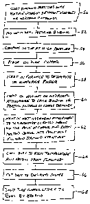
In a first step 50 of the method of Fig. 3, diamond particles are coated
with multiple layers of different elements or inorganic compounds.
Preferably, diamond powder, which is either synthetic or natural and which
has an average particle size between 20 microns and 120 microns, is coated
with multiple layers of different elements or inorganic compounds. The
coating method employed is ffuidized-bed chemical vapor deposition.
Optionally, autocatalytic (electrodeless) aqueous chemical plating can be
used. Sublayers of the coating may be deposited by one method and other
layers by the other method. Individual layers of the coating may be
comprised of elements or compounds taken from the group which includes Cr,
W, Mo, Co, Cu, Ti, Si, SiC, TiN, TiC, Ta and Zr. A preferred embodiment of
the diamond coating in accordance with the invention involves a four-layer
system in which the particles are first coated with a layer of Cr, followed by
a
6
CA 02505593 2005-05-06
WO 2004/044950 PCT/US2003/033945
layer of W, then a layer of Co, and then a layer of Cu. The thickness of each
layer is between 30 nanometers and 2 microns.
In a second step 52 shown in Fig. 3, the coated diamond particles are
mixed with a dry-pressing binder. Optionally, the particles may also be
mixed with copper powder.
In a third step 54 shown in Fig. 3, the particles are compacted in a die
at high pressure. Such pressure is preferably between 15,000 and 50,000
pounds per square inch.
In a fourth step 56 shown in Fig. 3, the body which results from
compaction is placed on top of a piece of pure copper and loaded into a
furnace.
In a fifth step 58 shown in Fig. 3, the body is heated in either vacuum -
or a wet hydrogen atmosphere to evaporate or thermally decompose the dry-
pressing binder. The heating is continued so that the body is exposed to at
least 700°C. for at least 10 minutes in a wet hydrogen atmosphere to
reduce
all copper oxides and to convert any carbonaceous residues on the copper or
on the diamond coating to CO or CO2.
In a sixth step 60 shown in Fig. 3, the compacted body is heated in a
vacuum or hydrogen atmosphere to cause bonding or partial sintering of the
coated diamonds. In this step, the compacted body is preferably heated to
950°C. for at least 10 minutes in either a vacuum or a hydrogen
atmosphere.
This causes bonding or "partial sintering" of the coated diamonds, causing
them to adhere to each other at points of contact.
In a seventh step 62 shown in Fig. 3, the body is heated in a wet or dry
hydrogen atmosphere to a temperature slightly above the melting point of
copper to draw melted copper into the partially sintered diamond structure.
This is preferably done at a temperature of 1200°C. The body is held
at this
temperature for at least 2 minutes.. When the copper melts, it is drawn by
capillary force into the partially sintered diamond compact. If the coating
system is effective, the .copper completely infiltrates the compact, leaving a
pore-free composite body. , .
7
CA 02505593 2005-05-06
WO 2004/044950 PCT/US2003/033945
In an eighth step 64 shown in Fig. 3, the body is cooled to room
temperature and removed from the furnace. In an optional step
corresponding to the step 64, the body is cooled to about 900°C., and
then the
furnace atmosphere is evacuated to a vacuum level of at least 1 x 10⁻⁴ torr.
It
is then re-heated above the copper melting point in vacuum and is held for at
least 15 minutes to remove dissolved hydrogen from the metal.
In a ninth step 66 shown in Fig. 3, the body is cut to a desired shape so
as to be usable in the package configurations shown in Figs. 1 or 2. Shaping
can be done by electric discharge machining (ED1VI) or by free-abrasive
lapping (using diamond abrasive), or a combination of the two.
In a tenth step 68 shown in Fig. 3, copper layers corresponding to the
layers 22 and 24 of Fig. 1 and 34 and 36 of Fig. 2 are bonded to the opposite
broad surfaces of the body of the. substrate, such as by brazing. .
In the case of the second embodiment of Fig. 2, further processing is
required in order to form the body 32 with the two different composites. In
this case, the copper/diamond composite insert 42 is bonded into the
surrounding copper/tungsten composite by re-melting it so as to allow the
copper matrices within each material to flow and intermingle.
The presently disclosed embodiments are therefore to be considered in
all respects as illustrative and not restrictive, the scope of the invention
being
indicated by the appended claims, rather than the foregoing description, and
all changes which come within the meaning and range of equivalency of the
claims are therefore intended to be embraced therein.
Y
..