Note: Descriptions are shown in the official language in which they were submitted.
CA 02507033 2008-11-26
77496-210
CLOSED LOOP TRANSMITTER CONTROL FOR POWER AMPLIFIER IN
AN EAS SYSTEM
BACKGROUND OF THE INVENTION
Field of the Invention
[0002] This invention relates generally to signal generation within an
electronic
article surveillance system and, more particularly, to a system and method for
amplifier control within a transmitter configured to transmit signals for
reception by
EAS tags.
Description of the Related Art
[0003] In acoustonlagnetic or magnetomechanical electronic article
surveillance, or
"EAS," a detection system may excite an EAS tag by transmitting an
electromagnetic
burst at a resonance frequency of the tag. When the tag is present within the
electromagnetic field created by the transmission burst, the tag begins to
resonate
with an acoustomagnetic or magnetomechanical response frequency that is
detectable
by a receiver in the detection system.
[0004] Transmitters used in these detection systems may include linear
amplifiers
using feedback control or switching amplifiers using open loop control. Linear
amplifiei-s provide good transmitter current regulation with feedback control,
but are
expensive because of poor power efficiency, typically around forty-five
percent
(45%). Pi-evious switching amplifiers provide good power efficiency, typically
around eighty-five percent (85%), but transmitter current levels can fluctuate
due to
the open loop control and variable load conditions.
[0005] Controller components of the prior art attempt to mitigate this current
fluctuation by providing a low bandwidth pulse width adjustment based on
measured
currents from previous transmission bursts. I.n one example, further described
below
-1-
CA 02507033 2008-11-26
77496-210
with respect to FIGS. I and 2, transmitter component hardware provides a
single
pulse width modulator that controls a single half bridge amplifier with
multiple loads
connected in parallel across the amplifier output. In this configuration, the
antenna
with the lowest impedance receives more current than antennas with higher
~ impedance, resulting in different levels of transmission, or power, being
output from
each of the antennas. Furthermore, the current sensing hardware in such prior
art
systems is such that only the current supplied to a single load can be sensed
at any
given time. Specifically, the current applied to a load is estimated after the
entire
transmission burst is completed by averaging the current samples.
CA 02507033 2008-11-26
77496-210
BRIEF DESCRIPTION OF THE INVENTION
In one aspect, there is provided a method for
controlling a transmitter in an electronic article
surveillance system, said method comprising: coupling each
of a plurality of transmit channels of the transmitter to a
corresponding antenna; configuring a modulator within each
transmit channel to output a modulated signal to the
corresponding antenna; providing feedback of each modulated
signal, adjusting operation of each modulator based on the
feedback, wherein adjusting operation of each modulator
comprises sensing an amount of current applied to the
corresponding antenna; converting the sensed current to a
digital value, configuring a proportional, integral,
differential control function to reduce an error between a
magnitude of the sensed current and a desired current value
and adjusting operation of the modulator comprises adjusting
a width of each pulse modulated signal applied to the
corresponding antenna, wherein a control value of the
control function is limited by a limiting function embodied
within a limiter to an allowable input range of the
modulator.
In another aspect, there is provided a transmitter
for an electronic article surveillance system comprising: a
plurality of antennas configured for transmission of
signals; and a plurality of transmit channels, each of said
transmit channels coupled to at least a corresponding one or
more of said antennas, each of said transmit channels
comprising: an amplifier configured to provide a signal to
the corresponding said antenna; a modulator configured to
provide a modulated signal to said amplifier; a sensing
circuit configured to sense an amount of current applied to
said antenna by said amplifier; and a controller configured
2a
CA 02507033 2008-11-26
77496-210
to receive the sensed current amount from said sensing
circuit, said controller configured to control operation of
said modulator based on the sensed current amount, said
controller comprising a mathematical component configured to
determine a magnitude of the sensed current; and a
proportional, integral, differential controller configured
to receive the sensed current magnitude and reduce an error
between the sensed magnitude and a desired current value,
wherein said modulator comprises a pulse with modulator,
coupled to the input of the amplifier and a limiter
connected between the output of the PID controller and said
modulator.
2b
CA 02507033 2008-11-26
77496-210
[0006] In one enibodirnent, a method foi- controlling a ti-ansmitter in an
electronic
article surveillance system is provided. The method mav comprise coupling each
of a
plurality of transmit charuiels of the transmitter to a corresponding antenna,
configuring a modulator within each transmit channel to output a modulated
signal to
the coi-responding antenna, providing feedback of each modulated signal, and
adjusting operation of each modulator based on the feedback.
[0007] In another embodiment, a transmitter for an electronic article
surveillance
system is provided. The transinitter may comprise a plurality of antennas
configured
l-or transmission of signals and a plurality of transmit channels. Each
transmit
channel is coupled to a corresponding one of the antennas, and each comprises
an
amplifier configured to supply a signal to its antenna, a modulator configured
to
supply a modulated signal to the amplifier, a sensing circuit configured to
sense an
amount of current applied to the antenna by the amplifier, and a controller
configured
to receive the sensed current amount fi-om the sensing circuit. The controller
is
contigured to controt operation of the modulator based on the sensed current
anlount.
[0008] In another embodiment, an electroriic article surveillance system is
provided
that may comprise at least one tag, at least one i-eceiver configured to
receive
emissions from the tag, and at least one transnlitter conlprising a plurality
oftransmit
channels. Each transmit channel may be configured to transnlit signals to
cause the
tag to resonate \~ hen the tac, is in a vicinitv of the transmit cllannel.
Each transmit
2c
CA 02507033 2005-05-10
channel may be independently configured to utilize feedback to control an
output
power of the transmit channel.
BRIEF DESCRIPTION OF THE DRAWINGS
[0009] For a better understanding of various embodiments of the invention,
reference should be made to the following detailed description which should be
read
in conjunction with the following figures wherein like numerals represent like
parts.
[0010] FIG. 1 is a block diagram of a known transmitter utilized in electronic
article
surveillance (EAS) systems.
[0011] FIG. 2 is a block diagram of a control function utilized within the
transmitter
of FIG. 1.
[0012] FIG. 3 is a block diagram of a transmitter incorporating independent
feedback control for each antenna load constructed in accordance with an
exemplary
embodiment of the invention.
[0013] FIG. 4 is a block diagram of an exemplary control function embodiment
for
use with the transmitter of FIG. 3.
[0014] FIG. 5 is a block diagram of an EAS system capable of incorporating the
transmitter of FIG. 3.
DETAILED DESCRIPTION OF THE INVENTION
[0015] For simplicity and ease of explanation, the invention will be described
herein in connection with various embodiments thereof. Those skilled in the
art will
recognize, however, that the features and advantages of the invention may be
implemented in a variety of configurations. It is to be understood, therefore,
that the
embodiments described herein are presented by way of illustration, not of
limitation.
[0016] FIG. 1 is a block diagram of a transmitter 10 for an electronic article
surveillance (EAS) system. Specifically, the transmitter 10 may include a
plurality of
antennas 12, 14, 16, and 18 respectively, that transmit a signal received from
an
amplifier 20. A controller 30 within the transmitter 10 may be configured to
provide
a low bandwidth pulse width adjustment based on current measurements taken
during
previous transmission bursts. In this embodiment, as illustrated in FIG. 1,
the
-3-
CA 02507033 2005-05-10
controller 30 may include a single pulse width modulator 32 that controls the
amplifier 20, which in one embodiment, may be a single half bridge amplifier,
with
the antennas 12, 14, 16, and 18 connected in parallel across amplifier output
22.
[0017] To provide control of the pulse width modulator 32, current sense
circuits
34, 36, 38, and 40 respectively, may be electrically connected to each
respective
antenna 12, 14, 16, and 18 and configured to sense an amount of current
delivered to
each respective antenna 12, 14, 16, and 18. The current sense circuits 34, 36,
38, and
40 each provide a measure of current applied to the antennas 12, 14, 16, and
18 to a
muxing circuit 42. The muxing circuit 42 may be controlled by a control
algorithm
component 44. The control algorithm component 44 determines which current
sense
circuit output is to be switched through muxing circuit 42 for processing by
an
analog-to-digital converter 46. Therefore, and in a sequence controlled by the
control
algorithm component 44, an amount of current applied to each antenna 12, 14,
16,
and 18 is fed back through the A/D converter 46 and the control algorithm
component
44 to control operation of the pulse width modulator 32.
[0018] However, in such a configuration the antennas 12, 14, 16, and 18
function as
a current divider, and the antenna with the lowest impedance receives more
current
than the antennas having higher impedances. The result is that each antenna
12, 14,
16, and 18 typically has a slightly different impedance and therefore
transmits a
different amount of power. This may be undesirable in an EAS system
transmitter.
Furthermore, the current sensing hardware in such a system (i.e., the current
sense
circuits 34, 36, 38, and 40 and the muxing circuit 42) is such that only the
current
applied to a single load (antenna) can be sensed at any one time. The current
applied
to each load is estimated after the transmission burst is completed by
averaging the
current samples received at the control algorithm 44.
[0019] FIG. 2 is a block diagram illustrating the functionality of the control
algorithm component 44. Specifically, a sample buffer 60 receives samples of
the
sensed current that is applied to the antennas 12, 14, 16, and 18 from the A/D
converter 46 (all shown in FIG. 1). As described above, sample buffer 60
receives
samples relating to a single one of antennas 12, 14, 16, and 18 at any one
time. The
-4-
CA 02507033 2005-05-10
samples are then processed to determine an amplitude of the samples by a
envelope
detector 62 as is known.
[0020] The amplitude of the sensed current sample is then input into a pulse
width
modulator control update equation 68. The pulse width modulator (PWM) control
values 70 receives inputs relating to a transmit frequency, phase of the
transmit
signal, and a desired current output of the PWM hardware. A calculation
component
72 may be configured to determine minimum PWM control values 70, sometimes
referred to as state variables, for the loads being driven by the PWM
hardware, via
amplifier 20 (shown in FIG. 1).
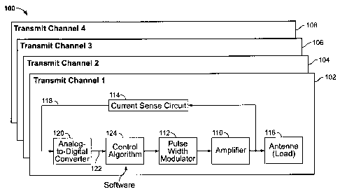
[0021] FIG. 3 is an illustration of an embodiment of a multiple channel
transmitter
100 for an EAS system that addresses the different antenna impedances and
resultant
variations in transmit power described above. In the illustrated embodiment,
four
independent transmitter channels 102, 104, 106 and 108 are illustrated, but it
is
understood that any number of transmitter channels may be utilized as
necessary for a
given EAS system application. In addition, while described with respect to
transmitter channel 102 below, it is to be understood that transmitter
channels 104,
106, and 108 may be similarly configured. In addition, any embodiments that
utilize
less than or more than four transmitter channels may be similarly configured.
[0022] In an exemplary embodiment, the transmitter 100 utilizes real-time
feedback
control of individual switching power amplifiers. As shown in the illustrated
embodiment, each transmitter channel, for example transmitter channel 102, may
include an independent switching amplifier 110 provided with real-time
feedback
control of the pulse width modulator 112. Such a configuration provides the
power
efficiency and low cost of switching amplifiers, with a level of current
regulation
similar to that commonly associated with linear amplifiers. Because the power
generated within each independent transmitter channel in this embodiment is
approximately one fourth the power generated within a transmitter using a
single
channel (and amplifier) to drive four antennas (e.g., transmitter 10 shown in
FIG. 1),
the electronic components utilized within transmitter channels 102, 104, 106,
and
108, are smaller, dissipate less power, and are less expensive in total than
the
electronic components utilized in production of transmitter 10.
-5-
CA 02507033 2005-05-10
[0023] Referring again to FIG. 3, the transmitter channel 102 may include a
current
sensing circuit 114 configured to measure, or sense, an amount of current that
the
amplifier 110 supplies to drive the load provided by antenna 116. In one
embodiment, current sensing circuit 114 may be configured to output a voltage.
The
current sensing circuit 114 provides a feedback signal 118 (e.g., a voltage),
which
may be input into an analog-to-digital converter (ADC) 120 and converted to a
digital
signal 122. This digital signal 122 may be input into a control algorithm
component
124. Control algorithm component 124, includes, for example, a processing
chip,
such as a microprocessor, microcontroller or digital signal processor (DSP)
and the
programming associated therewith. In alternative embodiments, the control
algorithm
component 124 may be implemented using combinations of discrete electronic
components.
[0024] Operation of an embodiment of a control algorithm component 124 is
illustrated in FIG. 4. As shown in FIG. 4, the digital signal 122, which is
representative of the current sensed at the output of the amplifier 110, may
be input
into the control algorithm component 124. The control algorithm component 124
may be configured to determine the magnitude of the feedback signal. In the
illustrated embodiment, magnitude of the digital signal 122 may be determined
using
an envelope detector 130 as is known. Those of ordinary skill in the art will
appreciate that other known detectors may be used.
[0025] In addition, the magnitude of the digital signal 122 (output 140) may
be
input into a proportional, integral, derivative, or "PID", controller 150. In
the
embodiment illustrated, a desired current amplitude, represented by set point
152,
may be subtracted from the computed current amplitude (output 140), producing
an
error signal 154. The error signal 154 may then be multiplied by a
proportional gain
constant 160, or Kp, to produce the proportional control value 162, or Cp. The
error
signal 154 may also input into an integrator equation, shown as discrete
integrator
170 in FIG. 4, whose output 172 is multiplied by the integral gain constant
174, or Ki,
to produce the integral control value 176, or Ci. Finally, the error signal
154 may
also be input into a differentiator equation, shown as discrete differentiator
180 in
-6-
CA 02507033 2005-05-10
FIG. 4, whose output 182 may be multiplied by the derivative gain constant
184, or
Kd, to produce the differential control value 186, or Cd.
[0026] The three control component values 162, 176, and 186, or Cp, Ci, and
Cd,
may be summed to produce a overall control value 190, or C. This control value
190
may be limited by a limiting function embodied within limiter 192 to an
allowable
input range of the pulse width modulator 112. The resulting control signal 194
may
be input into the pulse width modulator 112 (shown in FIG. 3). Implementation
of
discrete integral and differentiator equations on digital signal processors
and other
processing components generally is known to those skilled in the art. Also,
selection
of suitable gain constants Kp, Ki, and Kd may be dependent on other parameters
of
the system, such as variable gains in the current sense circuit 114 and the
amplifier
110 due to variations in discrete electronic components.
[0027] Although described as a digital signal processor (DSP), the signal
processing
described herein is capable of being performed on microprocessors,
microcontrollers,
and other processing topologies, for example, fuzzy and/or neural control
structures,
observer/estimator or state space control structures, and other topologies,
without
altering the essence of the embodiments herein described. Also, advances in
semiconductor integration have produced a variety of integrated circuits that
integrate, for example, muxing, analog to digital conversion, and modulation
within a
single processor chip.
[0028] In operation, the control signal 194 generated by the control algorithm
component 124 is therefore based upon an amount of current sensed at the
antenna
116 by the current sense circuit 114 (both shown in FIG. 3). This control
signal 194
may be input into the pulse width modulator 112 (shown in FIG. 3), which
generates
a pulse modulated signal having a pulse width dependent upon the parameters of
the
control signal 194. The pulse modulated signal generated may then be amplified
by
the amplifier 110 (shown in FIG. 3) and used to drive the transmission antenna
116.
The transmission pulse output results in a current applied to the antenna 116.
The
current may again be sensed by current sensing circuit 114, which provides
feedback
to the control algorithm component 124. In this way, feedback is utilized to
set the
width of the transmitted signal pulse output by the amplifier 110.
-7-
CA 02507033 2005-05-10
100291 The EAS system transmitter 100 described with respect to FIGS. 3 and 4
provides independent real-time control of the amount of current applied to
multiple
antenna loads. As such, an EAS transmitter can be configured so that a desired
amount of transmit power can be individually controlled for each antenna of
the
transmitter 100 through simultaneous, independent, current monitoring of all
transmit
channels 102, 104, 106, and 108. As compared to, for example, transmitter 10
(shown in FIG. 1), cost of the transmitter is reduced to due semiconductor
integration
and also due to the reduction in power (both generated and dissipated)
associated with
separate transmit channels. A net effect of higher integration and smaller,
less
expensive power components is that the total cost of using multiple
independent
transmit channels and loads is less than using a single channel to supply
power for
multiple loads. In addition, the transmitter configurations described herein
also result
in advantages with respect to circuit protection, thermal management, and
current
regulation as compared to known transmitter configurations.
(0030] FIG. 5 is an illustration of an EAS system 200 which is capable of
incorporating the embodiments of transmitter 100 described herein.
Specifically,
EAS system 200 may include a first antenna pedesta1202 and a second antenna
pedesta1204, each of which may include a number of antennas (e.g., antenna
16).
The antennas within antenna pedestals 202 and 204 may be connected to a
control
unit 206 that may include transmitter 100 and receiver 210. Within control
unit 206 a
controller 212 may be configured for communication with an external device. In
addition, controller 212 may be configured to control the timing of
transmissions
from transmitter 100 and expected receptions at receiver 210 such that the
antenna
pedestals 202 and 204 can be utilized for both transmission of signals to an
EAS tag
220 and reception of frequencies generated by EAS tag 220. System 200 is
representative of many EAS systems and is meant as an example only. For
example,
in an alternative embodiment, control unit 206 may be located within one of
the
antenna pedestals 202 and 204. In still another embodiment, additional
antennas
which only receive frequencies from the EAS tags 220 may be utilized as part
of the
EAS system 200. Also a single control unit 206, either within a pedestal or
located
separately, may be configured to control multiple sets of antenna pedestals.
-8-
CA 02507033 2005-05-10
[0031] As a result of incorporating the embodiments described herein, the
performance of the transmitters (e.g., transmitter 100) in EAS systems (e.g.,
EAS
system 200) is improved to provide an increase in power efficiency and to
allow the
independent sensing of multiple antenna loads. At the same time, such
transmitters
provide reliable transmitter current levels under variable load conditions and
also
provide redundant fault handling at a low cost.
[0032] It is to be understood that variations and modifications of the various
embodiments of the present invention can be made without departing from the
scope
of the invention. It is also to be understood that the scope of the various
embodiments of the invention are not to be interpreted as limited to the
specific
embodiments disclosed herein, but only in accordance with the appended claims
when read in light of the forgoing disclosure.
-9-