Language selection

Search

Patent 2507431 Summary

Third-party information liability

Some of the information on this Web page has been provided by external sources. The Government of Canada is not responsible for the accuracy, reliability or currency of the information supplied by external sources. Users wishing to rely upon this information should consult directly with the source of the information. Content provided by external sources is not subject to official languages, privacy and accessibility requirements.

Claims and Abstract availability

Any discrepancies in the text and image of the Claims and Abstract are due to differing posting times. Text of the Claims and Abstract are posted:

  • At the time the application is open to public inspection;
  • At the time of issue of the patent (grant).
(12) Patent: (11) CA 2507431
(54) English Title: SINGLE PACKAGE MULTI-CHIP RF POWER AMPLIFIER
(54) French Title: AMPLIFICATEUR DE PUISSANCE R.F. A MULTIPUCES EN PAQUET UNIQUE
Status: Term Expired - Post Grant Beyond Limit
Bibliographic Data
(51) International Patent Classification (IPC):
  • H03F 03/68 (2006.01)
  • H01L 23/66 (2006.01)
  • H01L 25/07 (2006.01)
  • H03F 03/60 (2006.01)
(72) Inventors :
  • PENGELLY, RAYMOND SYDNEY (United States of America)
  • WOOD, SIMON MAURICE (United States of America)
  • QUINN, JOHN PHILLIP (United States of America)
(73) Owners :
  • CREE, INC.
(71) Applicants :
  • CREE, INC. (United States of America)
(74) Agent: CASSAN MACLEAN IP AGENCY INC.
(74) Associate agent:
(45) Issued: 2013-01-15
(86) PCT Filing Date: 2003-11-24
(87) Open to Public Inspection: 2004-07-01
Examination requested: 2008-10-17
Availability of licence: N/A
Dedicated to the Public: N/A
(25) Language of filing: English

Patent Cooperation Treaty (PCT): Yes
(86) PCT Filing Number: PCT/US2003/037612
(87) International Publication Number: US2003037612
(85) National Entry: 2005-05-26

(30) Application Priority Data:
Application No. Country/Territory Date
10/318,849 (United States of America) 2002-12-13

Abstracts

English Abstract


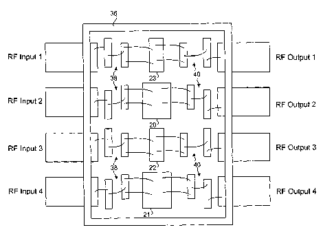
Disclosed are a multi-chip power amplifier comprising a plurality of chips (20-
23) with each chip being a transistor amplifier, and a housing (36) in which
all of the semiconductor chips are mounted. A plurality of input leads extend
into the housing and a plurality of output leads extend from the housing. A
plurality of first matching networks (38) couple a semiconductor chip to an
input lead and a plurality of second matching networks (40) couple each
semiconductor chip to an output lead whereby each chip has its own input lead
and output lead. By providing all amplifier chips within a single housing with
matching networks within the housing coupling the chips to the input and
output leads, manufacturing cost is reduced and the overall package footprint
on a mounting substrate is reduced. Further, the close proximity of the chips
within the housing reduces phase differences among signals in the
semiconductor chips.


French Abstract

L'invention concerne un amplificateur de puissance à multipuces comprenant une pluralité de puces (20-23) chaque puce consistant en un amplificateur à transistors, et un logement (36) dans lequel toutes les puces à semi-conducteurs sont montées. Une pluralité de fils d'entrée s'étend dans le logement et une pluralité de fils de sortie s'étend depuis le logement. Une pluralité de premiers réseaux d'adaptation (38) relie une puce à semi-conducteurs à un fil d'entrée et une pluralité de seconds réseaux d'adaptation (40) relie chaque puce à semi-conducteurs à un fil de sortie si bien que chaque puce possède son propre fil d'entrée et de sortie. Le fait de disposer toutes les puces d'amplificateur dans un seul logement avec des réseaux d'adaptation dans le logement reliant les puces aux fils d'entrée et de sortie, permet de réduire le coût de fabrication ainsi que tout l'espace occupé par le paquet sur un substrat de fixation. De plus, l'étroite proximité des puces dans le logement permet de réduire des différences de phase entre les signaux des puces à semi-conducteurs.

Claims

Note: Claims are shown in the official language in which they were submitted.


What is claimed is:
1. A multi-chip power amplifier comprising:
a) a housing having a plurality of housing input leads and a plurality of
housing
output leads,
b) a plurality of semiconductor chips mounted in the housing, each chip
comprising a transistor amplifier;
c) a plurality of first matching networks with each matching network coupling
a
semiconductor chip to a housing input lead; and,
d) a plurality of second matching networks with each network coupling a
semiconductor chip to a housing output lead whereby each chip has its own
housing input lead and housing output lead.
2. The multi-chip power amplifier of claim 1, further comprising:
a) a signal splitter for splitting an input signal into a plurality of
signals; and,
b) input coupling means for coupling each of the plurality of signals to a
respective housing input lead.
3. The multi-chip power amplifier of claim 1 or 2, wherein each chip comprises
a field
effect transistor having source, drain, and gate elements, a first matching
network
coupling a gate element to a housing input lead and a second matching network
coupling a drain element to a housing output lead.
4. The multi-chip power amplifier of claim 3 wherein the field effect
transistor is a
silicon LDMOSFET.
5. The multi-chip power amplifier of claim 3 wherein the field effect
transistor
comprises a MESFET.
6. The multi-chip power amplifier of claim 1 or 2 wherein each chip comprises
a bipolar
transistor having collector, base, and emitter elements, a first matching
network
coupling a base element to a housing input lead and a second matching network
coupling a collector element to a housing output lead.
4

7. The multi-chip power amplifier of claim 6 wherein the bipolar transistor
comprises a
silicon bipolar transistor.
8. The multi-chip power amplifier of claim 6 wherein the bipolar transistor
comprises a
III-V heterojunction bipolar transistor.
9. The multi-chip power amplifier of claim 6 wherein the bipolar transistor
comprises a
HEMT.
10. The multi-chip power amplifier of claim 1 or 2 wherein the power amplifier
is a
Doherty amplifier with one chip providing a carrier amplifier and at least one
chip
providing a peak amplifier.
11. The multi-chip power amplifier of claim 10 wherein a plurality of chips
provide peak
amplifiers with the peak amplifiers being biased to sequentially activate in
amplifying
an input signal depending on input signal amplitude.

Description

Note: Descriptions are shown in the official language in which they were submitted.


CA 02507431 2010-04-12
SINGLE PACKAGE MULTI-CHIP RF POWER AMPLIFIER
BACKGROUND OF THE INVENTION
[0002] This invention relates generally to a multi-chip RF power amplifier,
and more
particularly the invention relates to packaging a multi-chip RF power
amplifier.
[0003] Semiconductor power amplifiers typically comprise a plurality of
semiconductor
chips with each chip embodying a transistor amplifier, such as a silicon
laterally diffused
MOS field effect transistor (LDMOSFET). The transistor amplifiers can be
operated in
parallel to provide an increased power amplifier output, or the transistor
amplifiers can
comprise a main or carrier amplifier for maximum back-off power operation and
a
plurality of auxiliary or peak amplifiers which are suitably biased to begin
operation
sequentially for increasing power requirements. Such a power amplifier is
described in
U.S. Patent No. 6,700,444 issued 2 March, 2004
[0004] Conventional practice is to individually package each transistor
amplifier in a
housing, and then connect the packaged transistor amplifiers through impedance
matching networks and signal splitters to a common input. However, the use of
individual chip packages increases manufacturing costs and increases the total
package
footprint on a supporting substrate. Further, the mounting of several packages
necessarily
increases transistor spacing and signal phase differences between the
transistors.
BRIEF SUMMARY OF THE INVENTION
[0005] In accordance with the invention, a plurality of individual transistor
amplifier
chips are mounted within a single package with each chip having its own input
and
output leads. The chips can have unequal peripheries and gate widths, as often
employed
in a Doherty amplifier, and each chip can be pre-matched within the package
for its
input, output, and bias leads. The prematched transistor dice can then be used
in high-
efficiency amplifier designs, such as for carrier and peak amplifiers in a
Doherty
configuration.
[0006] The invention provides manufacturing efficiency and reduces the overall
packaging footprint. Further, the transistor dice are in close proximity
thereby
minimizing phase differences in signals in the several transistors. For a
Doherty
1

CA 02507431 2010-04-12
application, the package must have twice the number of leads as there are
chips in the
package. This allows each transistor to be individually pre-matched within the
package
and individually biased.
[00071 The invention and objects and features thereof would be more readily
apparent
from the following detailed description and dependent claims when taken with
the
drawings.
BRIEF DESCRIPTION OF THE DRAWINGS
[00081 Fig. 1 is a functional block diagram of an RP power amplifier for
amplifying an
RF signal over a broad range of power and employing a plurality of
individually
packaged power amplifiers as disclosed in U.S. Patent No. 6,700,444.
[00091 Fig. 2 is a plan view of an equivalent power amplifier to the amplifier
of Fig.
I in accordance with an embodiment of the invention.
100101 Fig. 3 is a functional block diagram of the power amplifier of Fig. 2
connected as
a four-way Doherty amplifier.
DETAILED DESCRIPTION OF THE INVENTION
[00111 Fig. 1 is a functional block diagram of a power amplifier described in
U.S. Patent
No. 6,700,444 which employs a plurality of individually housed power amplifier
chips
including a carrier amplifier 20 and three peak amplifiers 21,22, 23, with the
peak
amplifiers connected through 90 transformers 24,25, 26, to an output load 28.
A 90
transformer 30 connects a four- way splitter 32 to carrier amplifier 20. By
setting the DC
bias on each of the peak amplifiers to appropriate values, the peak amplifiers
allow a
Doherty action to be extended. For each peak amplifier that is added above the
first, there
will be a corresponding increase of 6 dB in the power range over which the
peak
efficiency will be maintained. The four-way amplifier extends the range of
efficient
power to a theoretical value of 18 dB. Such extension is very important in
digital
communication systems using modulation schemes where the peak to average power
ratios can be as high as 13 dB. A. 120 watt peak amplifier can be provided by
a four-way
Doherty arrangement with each path (carrier and three peak amplifiers)
utilizing 30 watt
transistors.
2

CA 02507431 2005-05-26
WO 2004/055979 PCT/US2003/037612
[0012] The individual power amplifiers need not be of the same size and the
chips
can have unequal peripheries or gate widths. However, each power amplifier
must be
impedance matched to the input and appropriately biased so that sequential
operation
of the amplifiers is realized for a broad range of power operation.
[0013] Fig. 2 is a plan view of a package in accordance with the present
invention in
which the plurality of power amplifier chips 20-23 are mounted with housing
36.
Each of the chips has its own input lead (RF input 1 - RF input 4) and output
lead (RF
output 1 - RF output 4). Further, each of the transistor chips 20-23 has its
own
impedance matching shown generally at 38 for the input, and shown generally at
40
for the output, and individually biased both for the gate and drain for a FET
(base and
collector for a bipolar device). Thus, for a Doherty arrangement the
individual
transistors can be matched differently and optimally as carrier and peaking
amplifiers
respectively.
[0014] Fig. 3 illustrates the four-transistor package 36 of Fig. 2 in a four-
way
Doherty amplifier. An RF input signal is applied through two-way splitters 50,
52, 54
to develop four input signals which are then applied through impedance
matching
circuitry 56 to the RF inputs of package 36. The outputs of the packaged
amplifier 36
are applied through impedance matching circuitry shown generally at 58, and
then
summed as the RF output at 60.
[0015] The use of a single housing for a multi-transistor chip amplifier with
individual leads provided in the housing for each amplifier chip not only
lowers
manufacturing costs, but the close proximity of the chips minimizes phase
differences
between the transistors. Additionally, the single housing reduces the
amplifier
footprint on a supporting substrate. While a four-chip Doherty amplifier has
been
described, the invention is readily applicable to a Doherty amplifier having a
carrier
amplifier and a single peak amplifier. Further, the invention is applicable to
multistage amplifier transistors. The invention can be implemented using a
wide
range of semiconductor technologies including silicon bipolar, GaAs, MESFET,
InGaHBT, SiC MESFET, and GaN HEMT, over a wide range of power levels and
frequencies.
[0016] Thus, while the invention has been described with reference to specific
embodiments, the description is illustrative of the invention is not to be
construed as
limiting the invention. Various modification and applications may occur to
those
skilled in the art without departing from the true spirit and scope of the
invention as
defined by the appended claims.
3

Representative Drawing
A single figure which represents the drawing illustrating the invention.
Administrative Status

2024-08-01:As part of the Next Generation Patents (NGP) transition, the Canadian Patents Database (CPD) now contains a more detailed Event History, which replicates the Event Log of our new back-office solution.

Please note that "Inactive:" events refers to events no longer in use in our new back-office solution.

For a clearer understanding of the status of the application/patent presented on this page, the site Disclaimer , as well as the definitions for Patent , Event History , Maintenance Fee  and Payment History  should be consulted.

Event History

Description Date
Inactive: Expired (new Act pat) 2023-11-24
Common Representative Appointed 2019-10-30
Inactive: Agents merged 2018-02-05
Inactive: Office letter 2018-02-05
Grant by Issuance 2013-01-15
Inactive: Cover page published 2013-01-14
Pre-grant 2012-10-03
Inactive: Final fee received 2012-10-03
Notice of Allowance is Issued 2012-04-05
Letter Sent 2012-04-05
Notice of Allowance is Issued 2012-04-05
Inactive: Approved for allowance (AFA) 2012-03-29
Inactive: Adhoc Request Documented 2011-09-13
Inactive: Delete abandonment 2011-09-13
Letter Sent 2011-07-29
Inactive: Correspondence - Transfer 2011-07-15
Inactive: Abandoned - No reply to s.30(2) Rules requisition 2011-06-20
Amendment Received - Voluntary Amendment 2011-06-16
Inactive: S.30(2) Rules - Examiner requisition 2010-12-20
Amendment Received - Voluntary Amendment 2010-04-12
Inactive: S.30(2) Rules - Examiner requisition 2009-10-13
Amendment Received - Voluntary Amendment 2009-05-28
Inactive: Correspondence - PCT 2008-12-04
Letter Sent 2008-12-01
Request for Examination Received 2008-10-17
Request for Examination Requirements Determined Compliant 2008-10-17
All Requirements for Examination Determined Compliant 2008-10-17
Letter Sent 2006-09-26
Inactive: Correspondence - Transfer 2006-08-28
Inactive: Transfer information requested 2006-05-26
Letter Sent 2006-05-02
Inactive: Single transfer 2006-03-16
Inactive: IPC from MCD 2006-03-12
Inactive: Cover page published 2005-08-24
Inactive: Courtesy letter - Evidence 2005-08-23
Inactive: Notice - National entry - No RFE 2005-08-20
Application Received - PCT 2005-06-22
National Entry Requirements Determined Compliant 2005-05-26
Application Published (Open to Public Inspection) 2004-07-01

Abandonment History

There is no abandonment history.

Maintenance Fee

The last payment was received on 2012-11-09

Note : If the full payment has not been received on or before the date indicated, a further fee may be required which may be one of the following

  • the reinstatement fee;
  • the late payment fee; or
  • additional fee to reverse deemed expiry.

Patent fees are adjusted on the 1st of January every year. The amounts above are the current amounts if received by December 31 of the current year.
Please refer to the CIPO Patent Fees web page to see all current fee amounts.

Owners on Record

Note: Records showing the ownership history in alphabetical order.

Current Owners on Record
CREE, INC.
Past Owners on Record
JOHN PHILLIP QUINN
RAYMOND SYDNEY PENGELLY
SIMON MAURICE WOOD
Past Owners that do not appear in the "Owners on Record" listing will appear in other documentation within the application.
Documents

To view selected files, please enter reCAPTCHA code :


To view images, click a link in the Document Description column. To download the documents, select one or more checkboxes in the first column and then click the "Download Selected in PDF format (Zip Archive)" or the "Download Selected as Single PDF" button.

List of published and non-published patent-specific documents on the CPD .

If you have any difficulty accessing content, you can call the Client Service Centre at 1-866-997-1936 or send them an e-mail at CIPO Client Service Centre.


Document
Description 
Date
(yyyy-mm-dd) 
Number of pages   Size of Image (KB) 
Description 2005-05-25 3 197
Drawings 2005-05-25 3 40
Claims 2005-05-25 3 127
Representative drawing 2005-05-25 1 15
Abstract 2005-05-25 2 70
Description 2010-04-11 3 174
Claims 2010-04-11 2 57
Representative drawing 2012-12-30 1 11
Reminder of maintenance fee due 2005-08-21 1 110
Notice of National Entry 2005-08-19 1 193
Request for evidence or missing transfer 2006-05-28 1 101
Courtesy - Certificate of registration (related document(s)) 2006-09-25 1 105
Reminder - Request for Examination 2008-07-27 1 119
Acknowledgement of Request for Examination 2008-11-30 1 176
Commissioner's Notice - Application Found Allowable 2012-04-04 1 163
PCT 2005-05-25 10 420
Correspondence 2005-08-19 1 26
Fees 2005-11-23 1 27
Correspondence 2006-05-25 1 23
Correspondence 2008-12-03 1 34
Correspondence 2011-06-28 1 14
Correspondence 2012-10-02 1 52
Courtesy - Office Letter 2018-02-04 1 32
Prosecution correspondence 2009-05-27 1 47