Note: Descriptions are shown in the official language in which they were submitted.
CA 02507533 2005-05-27
WO 2004/061497 PCT/US2003/035257
PROCESS FOR FABRICATION OF OPTICAL WAVEGUIDES
BACKGROUND OF THE INVENTION
This invention relates to integrated optical circuit fabrication, and more
particularly to a novel process for fabrication of optical waveguides, whereby
lift-
off, rather than etching, is used to pattern the waveguide core.
Products based on so-called planar lightwave circuits (PLCs) have the
possibility of significantly reducing the cost and size of optical components,
while
at the same time enhancing functionality. Notable in this area is the work on
doped Si02 glass (See, e.g., M. Kawachi, Optical and Quantum Electronics 22
l0 (1990) 391-416). These low-doped glassy waveguide structures are similar to
well-known silica optical fibers with respect to optical guiding and hence
have
similar modal fields resulting in low coupling losses between the chip and
standard
single mode fiber.
However, an inherent disadvantage of these low-index-contrast glassy
15 structures is a rather large minimum radius of curvature allowable in
circuits,
typically greater than 15 mm. Devices containing many bends become very large,
such that only a small number of them may be arranged on a wafer, which is
less
cost-effective. In order to fabricate optical components in a more cost-
effective
way in mass production, it is desirable to increase the device density.
20 Figure 1 illustrates schematically the steps in an exemplary conventional
process for manufacturing channel waveguides 10. As illustrated in Figure la,
a
silicon substrate 12 is first provided and a lower cladding layer 14 is
deposited on
its upper surface. Refernng to Figure lb, a core layer 16 is deposited on top
of the
cladding layer. The cladding layer 14 and core layer 16 may be deposited by
25 various methods, such as flame hydrolysis deposition (FHD), chemical vapor
deposition (CVD), plasma-enhanced CVD (PECVD), sol-gel, etc. An example for
high index contrast material for fabrication of planar waveguides may be found
in
PCT publication WO 99/54714, where SiON and SiOz are used as a core and
cladding layers, respectively.
30 An alternative embodiment includes a lower optical cladding comprising a
substrate of a transparent material having an appropriate index, such as a Ge
doped
Si02 core on an undoped fused quartz substrate.
-1-
CA 02507533 2005-05-27
WO 2004/061497 PCT/US2003/035257
In the next step (Figure 1 c), the core layer 16 is annealed. Following core
layer annealing (Figure 1 d), a photoresist or metal mask 18 is coated over
the core
layer 16. Photolithography (Figure 1 e) and reactive ion etching (RIE) (Figure
1 f)
are used to define the desired ridge structure. The photoresist or metal mask
18 is
stripped as illustrated in Figure lg. Finally, Figure lh illustrates
deposition of an
upper cladding layer 20.
As seen in Figure l, conventional etching processes require a large number
of steps. RIE in particular is a time-consuming step in processing. RIE also
may
produce wall roughness that may lead to scattering loss in the resulting
channel
l0 waveguide. Additionally, conventional methods require significant capital
investment to provide necessary equipment and processes.
Given the difficulties with traditional etching, other methods used in
integrated circuit manufacturing have been attempted. However, there have been
difficulties, such as tearing or damage, applying these methods to the
fabrication of
optical waveguides.
The desire remains for a more efficient and cost-effective method for
fabrication of optical waveguides.
SUMMARY OF THE INVENTION
A method for manufacturing an optical waveguide device in accordance
2o with the present invention includes the steps of depositing a lower
cladding layer;
coating a photoresist layer directly on the lower cladding layer; patterning
the
photoresist layer to create channels; depositing a core layer, wherein a first
portion
of the core layer is deposited inside the channels and a second portion
overlays the
patterned photoresist layer; removing the patterned photoresist layer and the
second portions of the core layer overlaying the patterned photoresist layer;
and
depositing an upper cladding layer.
The optical waveguide may be a single-mode waveguide. The lower
optical cladding may include a substrate of a transparent material having an
appropriate index.
Alternatively, the lower cladding layer may include a Ge doped Si02 core
on an undoped fused quartz substrate, silicon dioxide (Si02), Magnesium
Fluoride,
diamond-like glass (DLG); polymers (acrylate, polyimide, silicon oxynitride
-2-
CA 02507533 2005-05-27
WO 2004/061497 PCT/US2003/035257
(SiON), and hybrid organic/inorganic sol-gel materials or boron- or fluorine-
doped Si02. The optical core layer may have a thickness between 0.2
micrometers
and 10 micrometers inclusive and include materials selected from one of the
following: silicon dioxide doped with titanium, zirconium, germanium,
tantalum,
hafnium, erbium, phosphorus, silver, nitrogen, or a sputtered multicomponent
glass.
In one embodiment of the present invention, the index of refraction
difference between the core layer and the cladding layer is about 0.3 %. The
optical core layer has a thickness of about 6.5 micrometers and an index of
1o refraction difference between the core layer and the cladding layer of
about 0.5%.
The step of patterning the photoresist layer may include photolithography
and the step of depositing the core layer may comprise plasma enhanced
chemical
vapor deposition or sputtering. Alternatively, the steps of depositing may
include
one of the following: physical vapor deposition (PVD), sputtering,
evaporation,
electron beam evaporation, molecular beam epitaxy, pulsed laser deposition,
flame
hydrolysis deposition (FHD), and more preferably chemical vapor deposition
including atmospheric pressure chemical vapor deposition (APCVD), low-pressure
chemical vapor deposition (LPCVD), and plasma-enhanced chemical vapor
deposition (PECVD).
2o Additionally, the method may include the step of etching the lower
cladding in a way that undercuts the photoresist. The step of etching the
lower
cladding may including the step of using an isotropic or anisotropic etchant
after
the step of patterning the photoresist.
Also, the method may include the step of providing a substrate base layer
on which to deposit the lower cladding layer. The substrate base layer may
comprise silicon, quartz, or a multicomponent glass. The method also may
include
the step of annealing the optical waveguide.
In one particular embodiment, the cladding includes SiOZ and the core
includes SiOz doped with Ge, P, Ti, or N.
3o BRIEF DESCRIPTION OF THE DRAWINGS
Figure 1 is a schematic step-wise illustration of a conventional method for
manufacturing channel optical waveguides.
-3-
CA 02507533 2005-05-27
WO 2004/061497 PCT/US2003/035257
Figure 2 is a schematic step-wise illustration of a method in accordance
with the present invention for manufacturing channel optical waveguides.
Figure 3 is a schematic step-wise illustration of a second embodiment
Figure 4 is schematic view of Si02/SiON/Si02/Si waveguide structures in
accordance with the present invention.
Figure 5 is an optical microscope photograph of exemplary waveguide
ridges formed by a first lift-off process in accordance with the present
invention.
Figure 6 is an optical microscope photograph of exemplary waveguide
ridges formed by a first lift-off process in accordance with the present
invention.
1o Figure 7 is a scanning electron microscope (SEM) microphotograph of
exemplary waveguide core ridge formed by a first lift-off process in
accordance
with the present invention.
Figure 8 is an SEM microphotograph of exemplary waveguide core ridge
formed by a first lift-off process in accordance with the present invention.
15 Figure 9 is the single mode output intensity measured of a 6.5 ~m
waveguide channel manufactured in accordance with the present invention.
Figure 10 is an optical microscope photograph of exemplary waveguide
core ridge formed by a first lift-off process in accordance with the present
invention.
20 Figure 11 is an optical microscope photograph of exemplary waveguide
ridges formed by a second lift-off process in accordance with the present
invention.
Figure 12 is an optical microscope photograph of exemplary waveguide
core ridge formed by a second lift-off process in accordance with the present
invention.
25 Figure 13 is an optical microscope photograph of exemplary waveguide
core ridge formed by a second lift-off process in accordance with the present
invention.
Figure 14 is an optical microscope photograph of exemplary waveguide
ridges formed by a third lift-off process in accordance with the present
invention.
30 Figure 15 is an optical microscope photograph of exemplary waveguide
core ridge formed by a third lift-off process in accordance with the present
invention.
-4-
CA 02507533 2005-05-27
WO 2004/061497 PCT/US2003/035257
Figure 16 is an optical microscope photograph of exemplary waveguide
core ridge formed by a third lift-off process in accordance with the present
invention.
DETAILED DESCRIPTION OF THE INVENTION
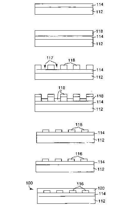
Figure 2 illustrates the steps in an exemplary new process in accordance
with the present invention for fabricating channel waveguides. A lift-off
technique, rather than etching, is used to pattern the waveguide core. This
new
process may significantly reduce processing time and steps and improve process
throughput and quality, thereby reducing chip cost. This new technique also
may
apply widely both to various high index contrast materials and to low index
contrast materials for the fabrication of optical integrated circuit devices.
Figure 2g and Figure 4 illustrate exemplary channel waveguides
manufactured in accordance with the present invention. Refernng to Figure 2g,
such a waveguide 100 includes a substrate 112, a lower cladding layer 114, a
core
layer 116, an upper cladding layer 120. Appropriate compositions and
thicknesses
of the core layer, lower cladding layer, upper cladding layer, and any
additional
layers) may be designed through numerical modeling. One well-known
waveguide modeling technique is the "transfer-matrix" approach (see, for
example,
Guided-Wave Optoelectronics, Theodor Tamir (Ed.), 2nd Edition, Springer-
2o Verlag). Alternatively, commercial waveguide modeling tools may be used,
including OptiBPM, from OptiWave Corporation, Ottawa, ON, Canada. Figure 4
illustrates an exemplary optical chip 300 having SiON channel waveguides
manufactured in accordance with the process of the present invention. The
channel
waveguide includes a lower cladding 314 of SiOz, having a thickness of 6.5
Vim,
and a refractive index n = 1.48 on a Si (100) wafer substrate 312. The core
316
includes SiON at a thickness of 1.2 p,m and a refractive index n = 1.6922. The
upper-cladding 320 includes Si02 with a thickness of 5.4 pm and a refractive
index
n = 1.48.
The exemplary manufacturing process begins as illustrated in Figure 2a,
3o which is similar to Figure la. A silicon substrate wafer 112, such as Si
(100), is
provided and lower cladding layer 114 is deposited on an upper surface of the
silicon substrate 112. Alternative substrate materials include quartz, or a
-5-
CA 02507533 2005-05-27
WO 2004/061497 PCT/US2003/035257
multicomponent glass. Suitable cladding materials include SiON, Si02,
Magnesium Fluoride, diamond-like glass (DLG); polymers (acrylate, polyimide;
silicon oxynitride (SiON); and hybrid organic/inorganic sol-gel materials or
boron-
or fluorine-doped Si02, and other suitable materials known in the art.
The cladding layer 114 may be deposited by methods known in the art,
such as flame hydrolysis deposition (FHD), chemical vapor deposition (CVD),
plasma-enhanced CVD (PECVD), sol-gel, sputtering, or vacuum evaporation.
In a particular exemplary process, SiOz is used as a lower-cladding. The
lower cladding layer 114 is deposited by PECVD technique using a reactor (such
1o as those commercially available as Plasmalab ~P made by Plasma Technology,
a
member of the Oxford Instruments Group, Bristol BS49 4AP UK) with parameters
as follows:
Deposition temperature: 300 °C
SiH4 flow: 3 sccm
N20 flow: 100 sccm
Deposition pressure: 50 mTorr
RF power (13.56MHz): 200 W
The above parameters were designed to achieve a cladding refractive index
of 1.48. Deposition time may vary depending on the thickness required for the
lower-cladding.
In the next step, illustrated in Figure 2b, of the present exemplary method, a
thick layer of photoresist 118 is applied directly over the cladding layer.
This is in
contrast with the traditional step illustrated in Figure lb of depositing a
core layer
16. In an exemplary embodiment, the silicon wafers 112 with the lower-cladding
114 were spin coated with a photoresist, such as positive Shipley 1818
(available
from the Shipley Company, Marlborough, MA 01752, USA). Other photoresists,
both positive and negative, may be used in this process.
The photoresist layer 118 is patterned, as illustrated in Figure 2c, by
conventional methods such as via exposure and development to obtain a
patterned
photoresist on the lower-cladding. The patterning creates vias 117 that expose
portions of the cladding layer 114.
-6-
CA 02507533 2005-05-27
WO 2004/061497 PCT/US2003/035257
Figure 2d illustrates the deposition of a core layer 116 over the patterned
photoresist layer 118. In an exemplary embodiment, a core layer of SiON is
deposited on patterned photoresist by PECVD technique with parameters as
follows:
Deposition temperature: 80°C
SiH4 flow: 8 scan
N20 flow: 20 scan
NH3 flow: 40 scan
Deposition pressure: 50 mTorr
to RF power: 200W
Application of the above parameters, is designed to yield a SiON film core
layer 116 having a thickness of 1.2 pm and a refractive index of 1.6922. SiON
is
exemplarily chosen as a core layer since its refractive index may be tuned
over a
wide range (n = 1.46-2.00) resulting in a large degree of freedom in
integrated
optics design. Alternative materials include high index contrast materials
such as
Si3N4, Ti-, Zr-, Hf , or Ta-doped Si02, suitable ferroelectric materials,
silicon
dioxide doped with titanium, zirconium, germanium, tantalum, hafnium, erbium,
phosphorus, silver, nitrogen, or a sputtered multicomponent glass such as
lanthanum-aluminum-zirconate system ("LAZ").
Figure 2e illustrates lift-off of the photoresist layer 118. After the
deposition of the core layer 116, the photoresist 118 is lifted off, such as
in a
photoresist stripper. The lift-off technique removes the portions of the core
layer
116 over the photoresist layer 118, leaving behind only the portions of the
core
layer 116 that rested inside of the channel vias 117.
Traditionally, the use of lift-off techniques for manufacturing optical
waveguides had been avoided. Attempts to apply traditional lift-off process to
lift-
off of waveguide materials by sputtering technique took a long time (several
hours
or over 10 hours) to achieve a thicker waveguide material layer. The
photoresist
layer was cross-linked by plasma during long sputtering process and thus
removal
of the photoresist layer without damaging the underlying layers was very
difficult.
In contrast, embodiments of the present invention use a PECVD technique
which is capable of fast deposition (generally 10 to 60 min for our waveguide
CA 02507533 2005-05-27
WO 2004/061497 PCT/US2003/035257
materials) and low process temperatures. These avoid cross-linking the
photoresist, thus allowing lift-off removal.
As illustrated in Figures 5 and 6, different waveguide ridges 117 (2, 2.5, 3,
3.5, 4, up to 8.5 ~m in pairs and then 15, 25, 50, 100 p.m) may be formed.
Figure 7
shows a SEM cross section of a 5 p,m core ridge 116 manufactured in accordance
with the method of the present invention. It may be appreciated that a very
smooth
sidewall may be achieved by the lift-off process of the present invention.
The core layers 116 may then be annealed as illustrated in Figure 2f.
Finally, as illustrated in Figure 2g, the upper cladding layer 120 including
the same
or similar materials as the bottom cladding layer 114 is deposited over both
the
bottom cladding layer 114 and the core layer 116. In a particular embodiment,
the
upper-cladding 120 includes SiOZ and is deposited to a thickness of 5.4 pm by
PECVD at the same or similar parameters as the lower-cladding layer 114.
Figure
8 is a photograph of a SEM cross section of the growth profile of the upper-
cladding of a 5 mm waveguide channel manufactured in accordance with the
present invention.
Figure 9 shows the single mode output intensity for an exemplary 6.5 p,m
waveguide channel manufactured in accordance with the present invention. Core
ridge widths of channels below 8.5 pm are single mode at 1550 nm with the SiON
2o waveguide structure as shown in Figure 4, while ridge widths above 8.5 p.m
are
mufti-modal guides. The propagation loss was measured to be around 2.85 dB/cm,
which is a norrrial value for as-deposited SiON films.
Removal of the photoresist pattern may cause tearing at the edges of the
deposited patterned layer. To overcome this problem, the photoresist layer may
have a "reverse bevel" in it. Figure 3 illustrates steps in an exemplary
process in
accordance with the present invention where the photoresist layer is undercut
when
patterned. The steps illustrated in Figures 3a to 3c are similar to those
illustrated in
Figures 2a to 2c. A lower cladding layer 214 is deposited over a silicon wafer
212.
A photoresist layer 218 is then deposited over the cladding layer 214 and
patterned
3o to create channels 217.
As illustrated in Figure 3d, the present embodiment differs in that undercut
channels 219 are etched into the cladding layer 214. In general, it is
difficult to
_g_
CA 02507533 2005-05-27
WO 2004/061497 PCT/US2003/035257
achieve an undercut photoresist pattern since the edges of the photoresist
pattern
are rounded at the base and top of the pattern and generally the edges tend to
be
overcut rather than undercut (that is, the bevel at the photoresist edge is
often in the
wrong direction).
Figure 10 is a photograph that corresponds to the schematic cross-section
illustrated in Figure 3d. Following are exemplary parameters used in this step
of
the process according to the present invention. An 8 pm thick Si02 cladding
layer
214 was deposited on a Si wafer 212 by PECVD. A photoresist layer 218,
including a photoresist such as Shipley 1818, was coated at 4000 rpm to a
thickness of about 1.9 pm over the Si02 cladding layer 214. The photoresist
layer
218 cured at 105 degrees C for 30 min and then was exposed to light having an
energy density of about 182 mJ/cmz with a metal mask. Following a thirty-
second
development in MF319 developer and a thorough rise in de-ionized water, a
patterning of photoresist layer 218 was accomplished.
An isotropic etch was then performed on the exposed portions of the lower
cladding layer 214 under the following parameters:
Buffered HF: 1:6 (HF:NH4F)
Etch time: 5 min
Etch rate: 100 nm/min
2o An anisotropic etchant also may be used. Using the above parameters, a
0.5 ~.m etch depth on the Si02 was obtained (see channel 217), with etch
features
219.
Refernng now to Figure 3e, the core layer 216 is then deposited over the
photoresist layer 218 and the exposed portions of the lower cladding layer
214.
Figure 11 is a photograph of an actual exemplary 2.5 ~m SiON core layer 216
deposited on the etched areas 217 and the photoresist 218 by PECVD.
As illustrated in Figure 3f, the photoresist layer 218 is removed along with
the portions of the core layer 216 overlapping the ridges of the photoresist
layer.
Figure 12 shows SiON waveguide core ridges 216 after the removal of the
3o photoresist. It has been successfully demonstrated that more than 3 pm
thick core
layers may be fabricated by lift-off process with undercut. Thus, it is
possible to
apply this technique to low index contrast materials.
-9-
CA 02507533 2005-05-27
WO 2004/061497 PCT/US2003/035257
Finally, as illustrated in Figure 3h, an upper cladding layer 220 is deposited
over both the core ridges 216 and the lower cladding layer 214. Figure 13
shows
an actual exemplary 8 pm upper cladding deposited on the core layer by PECVD
process. The refractive index of both the lower and the upper claddings, 214
and
220, is 1.46 while the refractive index of the core ridges 216 is 1.55. A very
good
Si02 step coverage achieved by the present PECVD process may be appreciated.
The process of the present invention may be used in the manufacture of a
variety of optical waveguides. In yet another exemplary embodiment illustrated
in
Figures 14 to 16, a silicon substrate 312 was used. A 3 ~m thermal oxidized
SiOz
cladding layer 314 was deposited over the substrate 312. A photoresist layer
318,
including a suitable photoresist such as AZ4400 (Clariant Corporation,
Business
Unit Electronic Materials, 70 Meister Avenue, Somerville, NJ 08876) was coated
on the Si02 cladding layer 314 at 4000 rpm to a thickness of about 4.5 Vim.
The
photoresist layer 318 was cured at 110 °C for 200 seconds and then was
exposed to
light having an energy density of about 280 mJ/cmz with a metal mask.
Following
a 60 second development in a developer, such as AZ 400K (Clariant Corporation,
Business Unit Electronic Materials, 70 Meister Avenue, Somerville, NJ 08876),
and a thorough rise in de-ionized water, the shown patterning of the
photoresist
layer was accomplished.
The cladding layer was then isotropically etched under the following
parameters:
Buffered HF: 1:6 (HF:NH4F)
Etch time: 20 min
Etch rate: 75 nm/min
Using the above parameters, a 1.5 ~m etch depth of Si02 was obtained.
Referring to Figure 15, a S ~m layer of diamond-like glass (DLG) 316 was
deposited with the Si using a commercially parallel-plate capacitively coupled
plasma reactor (commercially available from PlasmaTherm, Inc. of St.
Petersburg,
Florida) on the etched area and the photoresist as shown in Fig. 2. The wafer
was
3o placed on the powered electrode during the deposition and DLG was deposited
under the following conditions:
-10-
CA 02507533 2005-05-27
WO 2004/061497 PCT/US2003/035257
Tetramethlysilane flow: SO scan
OZ flow: 200 scan
Deposition pressure: 97 mTorr
RF power (13.56 MHz) 600 Watts
s Deposition time: 100 minutes
It may be appreciated that the DLG material did not deposit significantly on
the sidewall of the photoresist, since a directional deposition process was
used.
Figure 16 presents DLG waveguide core ridges 316 after the removal of the
photoresist. A more than 5 ~m thick core layer may be fabricated using the
present
lift-off process with undercut. The ability to create deeper core ridges
allows the
use of the present technique with low index contrast materials.
The process of the present invention offers reduced steps and lower
manufacturing times than traditional methods. Use of the present invention may
significantly improve throughput and quality of optical waveguides, thereby
reducing device costs and potentially enabling penetration of waveguide
devices
into cost-sensitive applications.
Waveguides manufactured in accordance with the present invention may be
used in a variety of optical circuits such as a Mach-Zehnder interferometer, a
thermo-optical switch, an arrayed waveguide grating, a directional coupler, or
a
2o waveguide Bragg grating filter. Other uses include active waveguide devices
including waveguides fabricated from electrooptic materials. Examplary
electrooptic materials include electrically poled glasses.
Those skilled in the art will appreciate that the present invention may be
used in the fabrication of a variety of different optical structures. While
the present
invention has been described with reference to exemplary preferred
embodiments,
the invention may be embodied in other specific forms without departing from
the
scope of the invention. Accordingly, it should be understood that the
embodiments
described and illustrated herein are only exemplary and should not be
considered
as limiting the scope of the present invention. Other variations and
modifications
3o may be made in accordance with the scope of the present invention.
-11-