Note: Descriptions are shown in the official language in which they were submitted.
CA 02507684 2005-05-27
WO 2004/050170 PCT/US2003/038168
AMORPHOUS SELENIUM DETECTOR FOR TOMOTHERAPY
AND OTHER IMAGE-GUIDED RADIOTHERAPY SYSTEMS
STATEMENT REGARDING FEDERALLY SPONSORED
RESEARCH OR DEVELOPMENT
This invention was made with United States Government support awarded by the
National Institute of Health (NIH), under Small Business Innovation Research
(SBIR)
Grant Nos. 1 R43 CA79383-O1 and 2R44CA079383-02 The United States Government
has certain rights in this invention.
BACKGROUND OF THE INVENTION
The present invention relates generally to radiation detectors and more
particularly
to an amorphous selenium (a-Se) detector for use in medical and industrial
applications
for detecting high energy radiation, especially for use in tomotherapy and
other image-
guided radiotherapy systems.
Current available detector technologies are not adequate for high energy
radiation
detection applications. One of the fundamental limitations in high energy x-
ray detectors
is that the interaction cross-section of high-energy x-rays in matter is
significantly
reduced. This poses severe problems for megavoltage radiotherapy imaging
applications.
One either has to settle for poor contrast at a given resolution, or increase
the radiation
dose to the patient to enhance image quality. The lcey to improving image
quality is to
increase the probability of the x-ray interacting in the detector.
The current commercially available solid-state detector designs generally
incorporate a layer of converter material in front of the x-ray sensors in
order to increase
1
CA 02507684 2005-05-27
WO 2004/050170 PCT/US2003/038168
conversion efficiency. Examples of such techniques include adding an
intensifying
phosphor screen in some scintillator and camera based detectors, or adding a
thin layer of
high-density material in front of a flat panel amorphous selenium detector
system.
However, improvements from these prior art systems are quite limited due to
the stopping
of secondary electrons once the converter material reaches a certain
thickness.
None of the current commercially available detectors for radiological (digital
radiography or mammography) applications and lcilovoltage (kV) computed
tomography
(CT) applications possess all the desired characteristics for high energy
radiation
detectors. Currently, commercially available detectors are roughly divided
into two
categories: flat panel detectors for digital radiography and mammography, and
detectors
for 1cV CT scanners. The active sensors used in these detectors are either
scintillators
such as cesium iodine crystals, or direct charge conversion materials such as
amorphous
selenium. The flat panel detectors offer superb spatial resolutions, while the
detectors for
modern kV CT scanners are designed with extremely high detection efficiencies,
typically
above 90% for kV x-rays. The flat panel detectors are readout with thin film
transistors
(TFT), while the CT detectors are typically readout with photo diodes. The
sensor
thickness of the flat panel detectors is typically less than 0.5 rnln, while
the sensor
thickness of the CT detectors is typically 2 to 3 mm. At radiotherapy energies
the
conversion efficiency of a flat panel detector is about 0.5%, while the
conversion
efficiency of a typical CT detector with a 2 mm layer of cadmium tungstate
crystals
would be about 10%. Neither adequately meets the needs of high energy
radiotherapy
imaging applications.
2
CA 02507684 2005-05-27
WO 2004/050170 PCT/US2003/038168
Corrunercially available flat panel detectors are clearly not suitable for
high
energy or megavoltage (MV) imaging applications for the following reasons:
1) The quantum efficiency is too low because the thiclrness of the amorphous
selenium layer is often too thin, not providing enough converter material.
2) The signal-to-noise ratio and the readout dynamic range, typically 10 bits,
are too small for MV imaging applications. As a comparison, typical modern kV
readout
electronics have a dynamic range of 20 bits.
3) The readout frame rate, typically 30 Hz, is too low, which does not allow
the detector system to be readout on a per pulse basis. A related problem is
synchronization of the readout electronics. Per pulse acquisition requires
synchronization
to the linear accelerator (linac) pulse. Furthermore, to effectively collect
all the charge
from the amorphous selenium detector one needs an electric field of about 10
V/p.m
which, in this case, requires an applied voltage of 3kV.
4) The detectors may suffer signficant radiation damage after a large amount
of radiation exposure. The term "radiation damage" refers to a change in the
output
signal from a detector, typically becoming smaller, after the detector has
withstood a large
amount of radiation exposure. It is questionable if the TFT's employed in the
readout
electronics can survive the level of cumulative radiation exposure in a high
energy
radiation environment.
5) The pixel sizes are too small for megavoltage applications. At
megavoltage energies, the intrinsic blurring due to energetic secondary
electrons transport
3
CA 02507684 2005-05-27
WO 2004/050170 PCT/US2003/038168
limits achievable spatial resolution. These detectors may also be susceptible
to secondary
scattering.
The use of amorphous selenium is an x-ray imaging detector is well documented.
Significant effort has been devoted to using amorphous selenium for flat panel
applications in digital radiography and mammography. Using amorphous selenium
in the
present invention for megavoltage imaging is a brand new approach.
Amorphous selenium is a direct detector. An amorphous selenium detector
converts radiation directly into an electrical signal. Amorphous selenium is a
photoconductor that, when exposed to radiation, generates an electrical
current
proportional to the intensity of the radiation. This can lead to significantly
improved
detective quantum efficiency (DQE) compared to indirect detectors where the
ionization
is first converted into light and then back to an electronic signal, thereby
introducing
various losses in the process. Compared to gas ion chambers, selenium has a
density that
is thousands of times higher, allowing for much more compact detector designs,
especially at high energies. Selenium is a good insulator at room temperature
and has a
much smaller dark cmTent than semiconductor based detectors. Amorphous
selenium is
also resistant to radiation damage. All these characteristics are desired for
radiotherapy
imaging applications.
What is needed is a relatively simple, inexpensive, and high efficiency
radiation
detector suitable for high-energy tomotherapy and other image-guided
radiotherapy
imaging applications.
4
CA 02507684 2005-05-27
WO 2004/050170 PCT/US2003/038168
STJMMARY OF THE INVENTION
The present invention provides a megavoltage radiation detector for medical
and
industrial applications. The invention also provides a new technique that can
improve
detective efficiency of a detector for megavoltage x-rays significantly. The
concept of
incorporating a high density converter into a detector system is applicable
regardless of
the actual sensors used. This invention should also be applicable to any area
where high
efficiency in detecting high energy x-rays is required.
A detector assembly in accordance with a first embodiment of the present
invention includes an enclosure with a top, bottom, at least two sides, and at
least two
ends. The detector assembly further includes a plurality of detector elements
installed
within the assembly. The plurality of detector elements are preferably
vertically oriented
within the detector assembly. Each of the detector elements preferably
includes a
substrate, a readout electrode layer deposited on at least one surface of the
substrate, an
amorphous selenium layer deposited on at least one surface of the readout
electrode layer,
and a high voltage electrode layer deposited on at least one surface of the
amorphous
selenium layer. The detector assembly is preferably positioned within a
tomotherapy or
other image-guided radiotherapy machine such that the x-ray beam from the
radiation
source is directed downwardly and radially through the detector elements. And
an
electric field is applied transversely or perpendicularly across the detector
elements. The
readout electrode layer preferably includes a plurality of conductive strips
and gaps that
are oriented in various configurations, defining different embodiments that
cover the
whole radiation fan beam and line up with the x-ray source.
5
CA 02507684 2005-05-27
WO 2004/050170 PCT/US2003/038168
A detector assembly in accordance with a second embodiment of the present
invention includes an enclosure with a top, bottom, at least two sides, and at
least two
ends. The detector assembly further includes a plurality of detector elements
installed
within the assembly. The plurality of detector elements are preferably arc-
shaped and
horizontally oriented within the detector assembly. Each of the detector
elements
preferably includes a substrate, a readout electrode layer deposited on at
least one surface
of the substrate, an amorphous selenium layer deposited on at least one
surface of the
readout electrode layer, and a high voltage electrode layer deposited on at
least one
surface of the amorphous selenium layer. The detector assembly is preferably
positioned
within a tomotherapy or other image-guided radiotherapy machine such that the
x-ray
beam from the radiation source is directed downwardly and radially through the
detector
elements. And an electric field is applied transversely or perpendicularly
across the
detector elements. Again, the readout electrode layer preferably includes a
plurality of
conductive strips and gaps that are oriented in various configurations,
defining different
embodiments that cover the whole radiation fan beam and line up with the x-ray
source.
The present invention also contemplates a method of fabricating a megavoltage
radiation detector.
The present invention provides a detector assembly that has significantly
better
sensitivity in megavoltage applications. The detector readout of the present
invention is
synchronized with the x-ray pulses. It is also possible to readout signals on
a pulse-by-
pulse basis. The detector assembly of the present invention also has good
performance
6
CA 02507684 2005-05-27
WO 2004/050170 PCT/US2003/038168
under high radiation exposure rate and can be used in a radiotherapy
enviromnent without
suffering significant radiation damage or deterioration in performance.
The present invention has applications in tomotherapy systems, where imaging
with the tomotherapy beams (the energy, intensity and other operating
parameters of the
beam can vary) is performed. The detection efficiency of the x-ray beams with
the
present invention is significantly improved, and thus the ability of resolving
the objects is
also significantly improved. The imaging functions in a tomotherapy system
include pre-
treatment imaging for patient registration, in-treatment dynamic imaging for
imaging
guidance of the treatment, and post treatment imaging for dose reconstruction
and
treatment verification. -
The present invention may also be applied to portal imaging in conventional
intensity modulated radiotherapy and other conventional radiotherapy where
detecting
high energy x-ray beams (energy above 1 MeV) and imaging of the patient with
the
radiotherapy beams are necessary or beneficial. In these types of applications
the image
device is placed post-patient in a radiotherapy system where imaging with the
radiotherapy beam is performed for the propose of verifying the setup of the
treatment
delivery device and operation of the treatment delivering system. The imaging
mode can
be simple projection imaging, similar to the x-ray films, or it can be
tomography imaging
reconstruction techniques to derive 3-D information of the patient. As an
example, the
detector of the present invention may be easily adapted to standard C-arm
gantry medical
accelerators, providing these units with the capability of CT imaging. Used in
portal
7
CA 02507684 2005-05-27
WO 2004/050170 PCT/US2003/038168
imaging, the detector of the present invention provides tremendous improvement
to
image quality due to orders of magnitude improvement in detective efficiency.
It should be noted that the detector of the present invention works just as
well for
kV CT applications, even though the longitudinal length, along the beam
direction, of the
detector is a bit excessive. However, the detector of the present invention is
extremely
attractive for dual energy imaging applications.
The detector assembly of the present invention not only offers superior
performance in megavoltage applications but also offers great potential for
savings in
tomotherapy system manufacturing costs. The process of manufacturing detector
elements and the mechanical assembly is much simplified, lowering cost. The
main cost
savings of the detector system is the electronics, which are also much simpler
than prior
art systems since the amplitude of the signals in the present invention are
much larger.
The detector design of the present invention may also find industrial
applications
such as defect detection where manufactured items such as cast auto-parts or
airplane
parts are imaged with high energy x-ray beams for detecting internal
materialistic or
structural defects. Because of the radiological thickness of these parts, high
energy x-rays
are necessary to penetrate through the objects being imaged. Conventional
detectors are
limited in detection efficiency, leading to poor image qualities. The present
invention
provides a detector with improved image and spatial resolution. Spatial
resolution is
critical to detect small imperfections in these parts. Other industrial
applications for the
present invention include detection of foreign objects in food paclcages and
imaging of
8
CA 02507684 2005-05-27
WO 2004/050170 PCT/US2003/038168
live trees to ensure quality of lumber before malting decisions to cut down a
tree in the
lumber industry.
The detector of the present invention may also fmd potential applications in
many
areas where fast and efficient detection of high energy x-rays are needed. One
example is
homeland security such as port inspection, including reliably inspecting large
pieces of
luggage and other goods from ships, airplanes, and trucks requiring
penetrating power
and spatial resolution. Current prior art imaging devices used for border and
port
inspections are mostly low energy x-ray machines and are incapable of
penetrating
materially thick containers. Therefore, high energy x-ray detectors of the
present
invention may malce significant contributions in homeland security. Other
areas of
security-related applications include inspection of airport baggage,
inspection of nuclear
waste, and inspection of other large size containers, requiring high energy x-
rays.
The following is summary of the features of the detector system of the present
invention:
1) The detector provides high detective efficiency above 50% at tomotherapy
energies, about 2 MeV in mean energy. This requirement forms the basis of
attaining
good spatial and contrast resolution. As a comparison, older Xe gas detectors
for kV CT
scanners, about 60 I~eV in mean energy, operate with efficiencies on the order
of 70%
while modern solid-state detectors operate with efficiencies greater than 95%.
Prior art
portal image detectors used at MV energies only have efficiencies on the order
of 1%.
9
CA 02507684 2005-05-27
WO 2004/050170 PCT/US2003/038168
2) The detector is capable of withstanding high intensity radiation exposure
and is able to be exposed to a substantial amount of accumulated exposure
without
suffering significant deterioration in performance. A typical clinic facility
accumulates
about 100 to 200 kGy to the detector in a year. Typical dose rates are 3 Gy
per minute.
3) The detector is capable of operating in a fast pulsed enviromnent with a
typical repetition rate of about 300 Hz and is able to read out every pulse.
The afterglow
is small and stable and can be reliably correctable when necessary.
4) The detector is two-dimensional with reasonably fine spatial resolution,
and covers the largest beam settings in a tomotherapy system.
5) The detector response is linear, stable and immmze to general radiation and
electromagnetic radiation of a radiotherapy machine. The readout electronics
have a large
dynamic range, preferably 20 bits.
6) The manufacturing cost for the detector is low compared to prior art
detectors.
Various other features, obj ects, and advantages of the invention will be made
apparent to those skilled in the art from the following detailed description.
BRIEF DESCRIPTION OF THE DRAWINGS
FIG. 1 is a perspective view of an embodiment of a detector assembly in
accordance with the present invention;
CA 02507684 2005-05-27
WO 2004/050170 PCT/US2003/038168
FIG. 2 is a perspective view of the detector assembly of FIG. 1 with the top
of the
assembly removed;
FIG. 3 is an enlarged detailed view of an upper corner portion of the assembly
of
FIG. 2 taken from detail 3 of FIG. 2;
FIG. 4 is a top plan view of an embodiment of a detector element in accordance
with the present invention;
FIG. 5 is an enlarged detailed view of a portion of the detector element of
FIG. 4
talcen from detail 5 of FIG. 4;
FIG. 6 is an enlarged exploded view of the detector element of FIGS. 4 and 5;
FIG. 7 is an enlarged detailed view of an embodiment of a readout electrode
layer
of the detector element of FIG. 6;
FIG. 8 is an enlarged detailed view of another embodiment of a readout
electrode
layer of the detector element of FIG. 6;
FIG. 9 is a perspective view of another embodiment of a detector assembly in
accordance with the present invention with top, one side, and one end of the
assembly
removed;
FIG. 10 is a perspective view of the detector assembly of FIG. 9 with portions
of
the enclosure and dielectric spacers in phantom;
11
CA 02507684 2005-05-27
WO 2004/050170 PCT/US2003/038168
FIG. 11 is a cross-sectional view of the detector assembly of FIGS. 9 an 10
taken
along line 11-11 of FIG. 10;
FIG. 12 is an enlarged exploded view of another embodiment of a detector
element in accordance with the present invention;
FIG. 13 is an enlarged front plan view of another embodiment of a readout
electrode layer of the detector element of FIG. 12;
FIG. 14 is an enlarged detailed view of an embodiment of a readout electrode
layer of the detector element of FIG. 12 taken from detail 14 of FIG. 12; and
FIG. 15 is an enlarged detailed view of another embodiment of a readout
electrode
layer of the detector element of FIG. 12 taken from detail 15 of FIG. 13.
DETAILED DESCRIPTION OF THE INVENTION
Referring now to the drawings, FIGS. 1-3 illustrate different views of an
embodiment of a detector assembly 10 in accordance with the present invention.
The
detector assembly 10 is preferably housed in an enclosure 12 as shown in FIG.
1. The
enclosure 12 is preferably arc-shaped and comprises a top 14, bottom 16, at
least two
sides 18, 20, and at least two ends 22, 24. A high voltage bus bar 26 extends
from one of
the sides 18 for connection to a high voltage source (not shown). A first
dielectric
element 28 preferably extends around and supports the bus bar 26. The top 14
and
bottom 16 of the enclosure 12 aid in support and alignment of the detector
assembly 10
when installed in tomotherapy and other image-guided radiotherapy systems.
FIG. 2
shows the detector assembly 10 of FIG. 1 with the top 14 of the assembly
removed. A
12
CA 02507684 2005-05-27
WO 2004/050170 PCT/US2003/038168
plurality of detector elements 30 are installed within the assembly 10. A
second dielectric
element 32 is preferably attached to the upper inside surface of one of the
sides 20
opposite the side 18 having the first dielectric element 28 attached thereto
for supporting
and aligning the detector elements 30 between the first and second dielectric
elements.
The dielectric elements 28, 32 preferably include alignment features for
locating the
detector elements 30 within the assembly. In addition to the high voltage bus
bar 26 and
the plurality of detector elements 30, the enclosure 12 also houses signal
conditioning and
digitization electronics (not shown) for the assembly. FIG. 3 is an enlarged
detailed view
of an upper corner portion of the detector assembly 12 shown in FIG. 2 taken
from detail
3 of FIG. 2. FIG. 3 shows the first dielectl-ic element 28 supporting the high
voltage bus
bar 26, a high voltage connection 34 for the high voltage bus bar 26, and a
plurality of
wire connections 36 from each of the detector elements 30 to the high voltage
bus bar 26.
The detector assembly 10 preferably provides a large number of detector
elements
30 compared to the current commercially available multi-row kV CT scanner
detector
systems. The detector elements 30 are preferably vertically oriented within
the detector
assembly 10. The detector elements 30 are preferably arranged coincidentally
with a
diverging x-ray beam. The divergence is preferably maintained by the tapering
dielectric
element 32 on one side of the detector elements. The dielectric elements 28,
30 and the
substrate of the detector elements 30 provide electric isolation between
neighboring
layers of the detector elements.
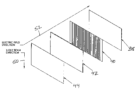
FIGS. 4-6 illustrate an embodiment of a detector element 30 in accordance with
the present invention. FIG. 5 is an enlarged detailed view of a portion of the
detector
13
CA 02507684 2005-05-27
WO 2004/050170 PCT/US2003/038168
element 30 of FIG. 4 talten from detail 5 of FIG. 4. FIG. 6 is an enlarged
exploded view
of the detector element 30 of FIGS. 4 and 5. The detector element 30
preferably
comprises a substrate 38, a readout electrode layer 40 deposited on at least
one surface of
the substrate 38, an amorphous selenium layer 42 deposited on at least one
surface of the
readout electrode layer 40, and a high voltage electrode layer 44 deposited on
at least one
surface of the amorphous selenium layer 42. Each of these layers is preferably
deposited
using vacuum deposition/evaporation or other suitable method. The substrate 38
is
preferably made of a glass material or other insulating material. The readout
electrode
layer 40 preferably comprises a plurality of conductive strips or lines 46
deposited on at
least one surface of the substrate as shov~m in FIG. 7. There are gaps or open
spaces 48
between the conductive strips or lines 46, again as shown in FIG. 7. The
amorphous
selenium layer 42 preferably comprises a uniform and continuous amorphous
selenium
material vapor deposited over the charge collection electrode layer 40. The
high voltage
electrode layer 44 is preferably of tungsten or other highly conductive
material that can
withstand high voltages.
As shown in FIG. 6, the x-ray beam 50 from the radiation source (not shown) is
directed downwardly and radially through the detector elements 30. An electric
field 52 '
is applied transversely or perpendicularly across the detector elements 30.
Therefore,
charge transport is constrained along the vertical field lines, significantly
reducing lateral
information spread. This means that the detector output closely matches the
input
radiation.
14
CA 02507684 2005-05-27
WO 2004/050170 PCT/US2003/038168
In a preferred embodiment, each detector element forms a pixel projecting to
lxl
mmz in area at the iso-center. The detector element is preferably fabricated
from a single-
sided substrate of about 0.25 mm thick. One side of the substrate preferably
includes
readout strips along the x-ray beam direction. The readout strips are
preferably about 1.4
mm wide separated from each other by a gap about 0.1 mm wide. The length of
the
detector element along the beam direction is preferably about 5 cm to achieve
50%
quantum efficiency. The height of the substrate is preferably about 8.5 cm. An
amorphous selenimn layer of approximately 1 mm thick is preferably deposited
on top of
the readout strips. A high voltage electrode tungsten layer of about 200 ~,m
is preferably
attached to the other side of the amorphous selenium layer, opposite the side
deposited on
top of the readout strips, forming the high voltage electrode layer. Care is
preferably
taken to ensure good conducting interface between the selenium and the
tungsten
surfaces. The high voltage electrode tungsten layer also serves as a converter
and septa
for rejecting very low energy photons resulted from secondary interactions in
and
upstream of the detector system. The x-ray beam enters the detector from the
top as
indicated in FIG. 6. The electric field lines point across the layers of the
detector
elements. Positive charges or holes are created in the tungsten or selenium
from a
primary photon interaction that is driven by the applied electric field
towards the
conducting readout strips on the substrate where they are collected. Each
readout
conducting strip on the substrate represents one detector. At a modest
thickness of the
amorphous selenium layer, less than 1 mm, and high electric field,
approximately 10
V/~.m, the spread of charge in the vertical direction, perpendicular to the
electric field
direction, is expected to be small, less than 100 ~,m. Therefore, the
separation between
CA 02507684 2005-05-27
WO 2004/050170 PCT/US2003/038168
the neighboring electrodes is preferably 100 Vim. The wide readout strips,
preferably 5
mm each, at the outer edges of the substrate are guard electrodes, which are
preferably
grounded to reduce electronic noise on the charge collection electrodes. Since
the energy
of the primary photon is high, the number of electrons per interaction will be
large. The
detector therefore, can probably be operated at a lower electric field, on the
order of 5
V/~m. This simplifies the complexity of the detector and the data acquisition
system of
the present invention.
FIG. 7 is an enlarged detailed view of an embodiment of a readout electrode
layer
of the detector element of FIG. 6. FIG. 8 illustrates an enlarged detailed
view of another
embodiment of a readout electrode layer of the detector element of FIG. 6. The
readout
electrode layer of FIG. 8 includes additional readout strips and gaps formed
perpendicular
to the original readout strips and gaps and perpendicular to the x-ray beam
direction.
This provides for more detailed and accurate detection of radiation.
An analysis of the required tolerances is important to optinuze cost and
performance of the present invention. The resolution of the photoetching of
the readout
electrode layer is preferably maintained to 5 ~,m. The thickness of the
amorphous
selenium layer is preferably maintained to 50 ~,m. These tolerances will
result in
interaction volume variation of about 5%. This will not affect the performance
because
the signal from each detector element will always be normalized to the signal
in that
detector element in the absence of a patient on a in tomotherapy and other
image-guided
radiotherapy system. The thickness of the high voltage electrode layer is
preferably
maintained to 25 ~,m. Local or global variations in the electrode layer or the
substrate
16
CA 02507684 2005-05-27
WO 2004/050170 PCT/US2003/038168
will not affect performance of the present invention because the thickness of
the layers
and the thickness of the separation will not influence the amount of charge
collected, and
small variations can be normalized out in the same fashion as for the active
detector
volume. The dielectric element thickness tolerance is preferably maintained to
2 Vim.
Random variations will not affect performance and systematic variations will
be evident
after all the layers are stacked and adjustments made. The tolerances of the
components
and layers can be easily maintained by modern machining and photoetching
technology.
The detector elements will be read out individually for every input radiation
pulse
with 16 bit integration analog-to-digital converters (ADCs). The digitizers of
the ADCs
are preferably equipped with a range selection bit to handle the big
difference in the
amplitudes of the output signals between the image and treatment mode of the
tomotherapy or other image-guided radiotherapy machine, leading to an
effective ADC
range of 20 bits. At a typical linac repetition rate of 300 Hz, the data rate
will be 25k x
2B x 300/s =151VIB/second, a fairly modest rate compared to modern kV CT
devices. As
stated above, the analog outputs from the detection elements are preferably
multiplexed to
digitizers. At the typical tomotherapy linac repetition rate, a level of
multiplexing of 500
to 1000 is possible, which reduces the number of digitizers from 25 to 50.
This helps to
reduce the manufacturing cost of the detector assemblies of the present
invention
substantially.
FIGS. 9-11 illustrate different views of another embodiment of a detector
assembly 60 in accordance with the present invention. FIG. 9 is a perspective
view of the
detector assembly 60 with the top, one side, and one end of the assembly
removed. FIG.
17
CA 02507684 2005-05-27
WO 2004/050170 PCT/US2003/038168
is a perspective view of the detector assembly 60 with portions of the
enclosure and
dielectric spacers in phantom. FIG. 11 is a cross-sectional view of the
detector assembly
60 talten along line 11-11 of FIG. 10.
The detector assembly 60 is preferably housed in an enclosure 62. The
enclosure
5 62 is preferably arc-shaped and comprises a top 64, bottom 66, at least two
sides 68, 70,
and at least two ends 72, 74. A high voltage connection 76 extends from at
least one end
of the detector elements 80 for connection to a high voltage source (not
shown). A
plurality of detector elements 80 are installed within the assembly 60. The
detector
elements 80 are also preferably arc-shaped and oriented horizontally within
the detector
10 assembly. A plurality of upper and lower dielectric elements 78 are
positioned on the top
and bottom of the detector elements 80 for supporting and aligning the
detector elements
80 within the detector assembly 60. The detector elements 80 are preferably
aligned
towards the radiation source (not shown). The enclosure 62 fiuther includes
signal
conditioning and digitization electronics (not shown) for the assembly.
FIG. 12 illustrates another embodiment of a detector element 80 in accordance
with the present invention. The detector element 80 preferably comprises a
substrate 82, a
readout electrode layer 84 deposited on at least one surface of the substrate
82, an
amorphous selenium layer 86 deposited on at least one surface of the readout
electrode
layer 84, and a high voltage electrode layer 88 deposited on at least one
surface of the
amorphous selenium layer 86. Each of these layers is preferably deposited
using vacuum
deposition/evaporation, photoetching, or other suitable method. The substrate
82 is
preferably made of a glass material or other insulating material. The readout
electrode
18
CA 02507684 2005-05-27
WO 2004/050170 PCT/US2003/038168
layer 84 preferably comprises a plurality of conductive strips or lines 90
deposited on at
least one surface of the substrate as shown in FIG. 14. There are gaps or open
spaces 92
between the conductive strips or lines 90, again as shown in FIG. 14. The
amorphous
selenium layer 86 preferably comprises a uniform and continuous amorphous
selenium
material vapor deposited over the charge collection electrode layer 84. The
high voltage
electrode layer 88 is preferably of tungsten or other highly conductive
material that, can
withstand high voltages. The substrate 82 provides electric isolation between
neighboring layers of the detector elements.
As shown in FIG. 12, the x-ray beam 94 from the radiation source (not shown)
is
directed downwardly and radially through the detector elements 80. An electric
field 96
is applied transversely or perpendicularly across the detector elements 80.
Each detector
element 80 consists of a plurality of different layers. Each layer will have a
certain
number of channels that cover the whole radiation fan beam in that plane. The
substrate
is preferably arranged to form an arc with traces lining up and converging to
the x-ray
source. The length of the traces will be optimized for maximum I?QE. FIG. 13
is an
enlarged front plan view of another embodiment of the readout elechode layer
84 of the
detector element of FIG. 12.
FIG. 14 is an enlarged detailed view of an embodiment of a readout electrode
layer of the detector element of FIG. 13. FIG. 15 illustrates an enlarged
detailed view of
another embodiment of a readout electrode layer of the detector element of
FIG. 13. The
readout electrode layer of FIG. 15 includes additional readout strips and gaps
formed
19
CA 02507684 2005-05-27
WO 2004/050170 PCT/US2003/038168
perpendicular to the original readout strips and gaps and perpendicular to the
x-ray beam
direction. This provides for more detailed and accurate detection of
radiation.
As shown in FIG. 15, the reading out of the signals from each electrode are
segmented along the beam direction of each channel. Each segment is attached
to
separated electronics and readout separately. By correlate the signals from
different
segments, information on dose deposition in the longitudinal direction (along
the x-ray
direction), thus the energy of the x-rays can be extracted.
In the above embodiments the traces of the electrodes can have a different
pitch
and width, depending on the need of the specific applications. The total
number of
chaimels in the vertical and horizontal directions can vary depending on the
application.
While the invention has been described with reference to preferred
embodiments,
it is to be understood that the invention is not intended to be linuted to the
specific
embodiments set forth above. It is recognized that those skilled in the art
will appreciate
that certain substitutions, alterations, modifications, and omissions may be
made without
departing from the spirit or intent of the invention. Accordingly, the
foregoing
description is meant to be exemplary only, the invention is to be taken as
including all
reasonable equivalents to the subject matter of the invention, and should not
limit the
scope of the invention set forth in the following claims.