Language selection

Search

Patent 2507719 Summary

Third-party information liability

Some of the information on this Web page has been provided by external sources. The Government of Canada is not responsible for the accuracy, reliability or currency of the information supplied by external sources. Users wishing to rely upon this information should consult directly with the source of the information. Content provided by external sources is not subject to official languages, privacy and accessibility requirements.

Claims and Abstract availability

Any discrepancies in the text and image of the Claims and Abstract are due to differing posting times. Text of the Claims and Abstract are posted:

  • At the time the application is open to public inspection;
  • At the time of issue of the patent (grant).
(12) Patent Application: (11) CA 2507719
(54) English Title: POWER SUPPLY CIRCUIT IN IC CHIP FOR NON-CONTACT IC CARD
(54) French Title: CIRCUIT D'ALIMENTATION DANS UNE PUCE A CI POUR UNE CARTE DE PROXIMITE A CI
Status: Deemed Abandoned and Beyond the Period of Reinstatement - Pending Response to Notice of Disregarded Communication
Bibliographic Data
(51) International Patent Classification (IPC):
  • G06K 19/07 (2006.01)
  • H02J 50/00 (2016.01)
(72) Inventors :
  • SUGIMURA, SHIRO (Japan)
  • KOBAYASHI, HIDEKI (Japan)
  • TANIGUCHI, SHUHEI (Japan)
(73) Owners :
  • FEC CO., LTD.
  • THE GOVERNMENT OF MALAYSIA
(71) Applicants :
  • FEC CO., LTD. (Japan)
  • THE GOVERNMENT OF MALAYSIA (Malaysia)
(74) Agent: MARKS & CLERK
(74) Associate agent:
(45) Issued:
(22) Filed Date: 2005-05-17
(41) Open to Public Inspection: 2006-11-17
Examination requested: 2005-05-17
Availability of licence: N/A
Dedicated to the Public: N/A
(25) Language of filing: English

Patent Cooperation Treaty (PCT): No

(30) Application Priority Data: None

Abstracts

English Abstract


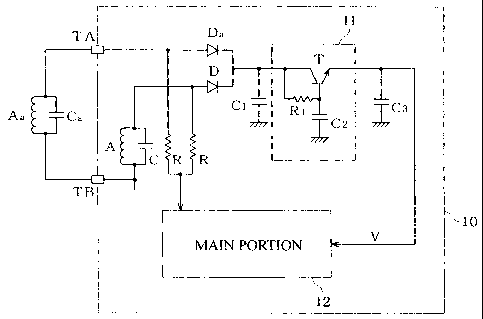
The capacitance of a smoothing capacitor is reduced, and
the size of an IC chip is minimized. A series transistor is
provided on the output side of a diode which rectifies the
output voltage of an antenna, and the smoothing capacitor is
connected to the base of the series transistor. If the current
gain of the series transistor T is .beta. then the apparent
capacitance of the smoothing capacitor C2 is multiplied by .beta..


Claims

Note: Claims are shown in the official language in which they were submitted.


What Is Claimed Is:
1. A power supply circuit in an IC chip for a non-
contact IC card, comprising:
an antenna;
a diode, which rectifies the output voltage of said
antenna;
a series transistor, inserted at the output side of said
diode; and,
a smoothing capacitor, connected to the base of said
series transistor; and wherein
said smoothing capacitor is formed integrally on the IC
chip, together with a main portion having memory functions and
communication functions.
2. The power supply circuit in an IC chip for a non-
contact IC card according to Claim 1, wherein said smoothing
capacitance has a capacitance on the order of several
picofarads.
3. The power supply circuit in an IC chip for a non-
contact IC card according to Claim 1 or Claim 2, wherein said
smoothing capacitor is realized through stray capacitance of
circuitry.
4. The power supply circuit in an IC chip for a non-
contact IC card according to Claim 1, wherein a supplementary
transistor supplying a base current is provided as an adjunct
to said series transistor.
8

5. The power supply circuit in an IC chip for a non-
contact IC card according to Claim 4, wherein said
supplementary transistor has a voltage-limiter function.
6. The power supply circuit in an IC chip for a non-
contact IC card according to Claim 1, wherein the output side
of said diode is connected to the output side of another diode
which rectifies the output voltage of an external antenna.
9

Description

Note: Descriptions are shown in the official language in which they were submitted.


- CA 02507719 2005-05-17
POWER SUPPLY CIRCUIT IN IC CHIP FOR NON-CONTACT IC CARD
BACKGROUND OF THE INVENTION
1. Field of the Invention
This invention relates to a power supply circuit in an IC
chip for a non-contact IC card, and in particular relates to a
power supply circuit in an IC chip for a non-contact IC card
enabling smaller capacitance of the smoothing capacitor and
reduced IC chip size.
2. Description of the Related Art
Non-contact IC cards are widely used. Such cards
incorporate an IC chip having memory functions and
communication functions into a card or sheet of base material,
and are capable of wireless data exchange with a reader/writer.
However, what are here called IC cards comprise, in addition
to so-called IC cards and IC tags, paper currency, securities
and similar incorporating IC chips.
Normally, the IC chip in an IC card receives carrier
radio waves from the reader/writer, and rectifies the waves to
generate an operating power supply voltage (as for example in
Japanese Patent Laid-open No. 2002-99886).
When using this technology of the prior art, there is
often the problem that, if the frequency of the carrier radio
wave from the reader/writer is low, the required capacitance
of the smoothing capacitor is large, and so the capacitor
1

CA 02507719 2005-05-17
cannot be mounted in the IC chip. For example, if the
frequency of the carrier radio wave is 13.56 MHz, the
capacitance of the smoothing capacitor is required to be 100
pF or greater, and it is physically impossible to mount a
capacitor with such a large capacitance on an IC chip
measuring approximately 0.5 mm on a side.
Hence one object of this invention is, in light of the
above problem of the prior art, to provide a power supply
circuit in an IC chip for non-contact IC cards having a
smaller smoothing capacitor capacitance and which can be
mounted without difficulty in an IC chip, even when the
frequency of the reader/writer carrier radio wave is low.
SUMMARY OF THE INVENTION
In order to achieve this object, a configuration of this
invention comprises an antenna, a diode for rectifying the
output voltage of the antenna, a series transistor inserted on
the output side of the diode, and a smoothing capacitor
connected to the base of the series transistor; the smoothing
capacitor is mounted integrally on the IC chip together with
the main portion having memory functions and communication
functions.
The smoothing capacitor can have a capacitance of order
several pF, and can be realized by stray capacitance in the
circuit.
2

CA 02507719 2005-05-17
Further, a supplementary transistor to supply a base
current may be provided as an adjunct to the series
transistor; the supplementary transistor may have voltage-
limiter functions.
Further, the output side of the diode may be connected to
the output side of another diode for rectifying the output
voltage of an external antenna.
By means of the configuration of this invention, the
smoothing capacitor connected to the base of the series
transistor need only have capacitance equal to 1/~ of the
capacitance of the smoothing capacitor when a series
transistor is not used (where ~ is the current gain of the
series transistor). That is, the series transistor increases
the equivalent capacitance of the smoothing capacitor, so that
a satisfactory ripple reduction effect can be obtained; when
the carrier radio wave frequency for the reader/writer is
13.56 MHz, the capacitance of the smoothing capacitor required
in the prior art, of 100 pF or greater, can be reduced to the
order of several pF, so that the capacitor can easily be
mounted integrally on the IC chip. Further, such a low-
capacitance smoothing capacitor can also be realized as stray
capacitance in the circuitry within the IC chip.
A supplementary transistor provided as an adjunct to the
series transistor supplies the base current to the series
transistor, and improves the stability of operation overall. A
3

CA 02507719 2005-05-17
supplementary transistor can also realize voltage-limiter
functions by limiting the base voltage to a fixed voltage.
If another diode is provided to rectify the output
voltage of an external antenna, the carrier radio wave
received from the reader/writer via the external antenna can
also be utilized as an operating power supply voltage, so that
the distance over which communication with the reader/writer
is performed can be increased. The external antenna is
incorporated within the base material and connected to a
terminal provided on the IC chip.
BRIEF DESCRIPTION OF THE DRAWINGS
Fig. 1 is an overall system diagram; and,
Fig. 2 is a system diagram showing principal portions in
another aspect.
DESCRIPTION OF THE PREFERRED EMBODIMENTS
Below, aspects of the invention are explained using the
drawings.
A power supply circuit in an IC chip for a non-contact IC
card comprises an antenna A, diode D, series transistor T, and
smoothing capacitors C1, C2, C3 (Fig. 1), and is formed
integrally on an IC chip 10 together with a main portion 12
having memory functions and communication functions.
4

CA 02507719 2005-05-17
The antenna A is connected to a capacitor C for parallel
resonance; the end of the antenna A on the ungrounded side is
connected through the diode D to the collector of the series
transistor T. The output side of the diode D is connected
through the terminal TA to the output side of another diode Da
connected to the end on the ungrounded side of an external
antenna Aa, and is also connected to a smoothing capacitor C1.
A resistance R1 is connected between the collector and base of
the series transistor T, and a smoothing capacitor C2 is
connected to the base of the series transistor T. The output
side of the series transistor T, that is, the emitter, is
connected to a smoothing capacitor C3, and the emitter of the
series transistor T is connected to the main portion 12.
The inputs of the diodes D and Da are connected, via
coupling resistances R, R, are combined and connected to the
main portion 12. The external antenna Aa is connected to a
capacitor Ca for parallel resonance, and the grounded end of
the external antenna Aa is connected through the terminal TB
to the grounded end of the antenna A.
When a carrier radio wave from a reader/writer, not shown,
arrives at one or both of the antenna A and the external
antenna Aa, the output voltages of the antenna A and external
antenna Aa are rectified by the diodes D, Da, and are smoothed
by the smoothing capacitor Cl. On the other hand, the series
transistor T acts as the equivalent of a smoothing capacitor
with capacitance equal to ~ times the capacitance of the
S

CA 02507719 2005-05-17
smoothing capacitor C2 (where a is the current gain of the
series transistor T), connected in parallel with the smoothing
capacitor C3. Hence even when the frequency of the carrier
radio wave from the reader/writer is 13.56 MHz, the
capacitance of the smoothing capacitor C2 need only be, at
most, of order several pF. The smoothing capacitors Cl and C3
are supplementary, and each need only be of order several pF.
Hence each of the smoothing capacitors C1, C2, C3 can
easily be realized as stray capacitances of the circuitry
within the IC chip 10, without the need to take special steps
to form capacitor devices within the IC chip 10. Moreover, a
sufficiently stable operating power supply voltage V is
generated on the output side of the series transistor T, so
that power can be supplied to the main portion 12.
In Fig. l, the circuit 11 comprising the series
transistor T may also be configured with a supplementary
transistor T1 added (Fig. 2).
The base and collector of the supplementary transistor T1
are connected through the resistors R1 and R2 respectively to
the collector of the series transistor T, and the base of the
supplementary transistor T1 is connected through a Zener diode
Z to ground. The emitter of the supplementary transistor T1 is
connected to the base of the series transistor T. Moreover, a
protection diode D1 is connected between the collector and
emitter of the series transistor T.
6

CA 02507719 2005-05-17
The supplementary transistor T1 realizes a voltage
limiter function through the Zener diode Z, and in addition
supplies a base current to the series transistor T, and so can
increase the effective current gain of the series transistor T,
and can contribute to stabilization of operation.
In the above explanation, the external antenna Aa and
capacitor Ca connected to the terminals TA and TB are
effective for broadening the distance of communication with
the reader/writer. An external antenna Aa and capacitor Ca
should be provided as necessary.
7

Representative Drawing
A single figure which represents the drawing illustrating the invention.
Administrative Status

2024-08-01:As part of the Next Generation Patents (NGP) transition, the Canadian Patents Database (CPD) now contains a more detailed Event History, which replicates the Event Log of our new back-office solution.

Please note that "Inactive:" events refers to events no longer in use in our new back-office solution.

For a clearer understanding of the status of the application/patent presented on this page, the site Disclaimer , as well as the definitions for Patent , Event History , Maintenance Fee  and Payment History  should be consulted.

Event History

Description Date
Inactive: IPC deactivated 2016-01-16
Inactive: IPC assigned 2016-01-01
Inactive: IPC expired 2016-01-01
Application Not Reinstated by Deadline 2011-05-17
Time Limit for Reversal Expired 2011-05-17
Deemed Abandoned - Failure to Respond to Maintenance Fee Notice 2010-05-17
Amendment Received - Voluntary Amendment 2010-01-20
Amendment Received - Voluntary Amendment 2009-12-07
Inactive: S.30(2) Rules - Examiner requisition 2009-06-10
Application Published (Open to Public Inspection) 2006-11-17
Inactive: Cover page published 2006-11-16
Inactive: IPC assigned 2005-09-12
Inactive: First IPC assigned 2005-09-12
Application Received - Regular National 2005-06-27
Letter Sent 2005-06-27
Inactive: Filing certificate - RFE (English) 2005-06-27
Request for Examination Requirements Determined Compliant 2005-05-17
All Requirements for Examination Determined Compliant 2005-05-17

Abandonment History

Abandonment Date Reason Reinstatement Date
2010-05-17

Maintenance Fee

The last payment was received on 2009-04-07

Note : If the full payment has not been received on or before the date indicated, a further fee may be required which may be one of the following

  • the reinstatement fee;
  • the late payment fee; or
  • additional fee to reverse deemed expiry.

Patent fees are adjusted on the 1st of January every year. The amounts above are the current amounts if received by December 31 of the current year.
Please refer to the CIPO Patent Fees web page to see all current fee amounts.

Fee History

Fee Type Anniversary Year Due Date Paid Date
Registration of a document 2005-05-17
Application fee - standard 2005-05-17
Request for examination - standard 2005-05-17
MF (application, 2nd anniv.) - standard 02 2007-05-17 2007-04-23
MF (application, 3rd anniv.) - standard 03 2008-05-20 2008-04-10
MF (application, 4th anniv.) - standard 04 2009-05-19 2009-04-07
Owners on Record

Note: Records showing the ownership history in alphabetical order.

Current Owners on Record
FEC CO., LTD.
THE GOVERNMENT OF MALAYSIA
Past Owners on Record
HIDEKI KOBAYASHI
SHIRO SUGIMURA
SHUHEI TANIGUCHI
Past Owners that do not appear in the "Owners on Record" listing will appear in other documentation within the application.
Documents

To view selected files, please enter reCAPTCHA code :


To view images, click a link in the Document Description column. To download the documents, select one or more checkboxes in the first column and then click the "Download Selected in PDF format (Zip Archive)" or the "Download Selected as Single PDF" button.

List of published and non-published patent-specific documents on the CPD .

If you have any difficulty accessing content, you can call the Client Service Centre at 1-866-997-1936 or send them an e-mail at CIPO Client Service Centre.


Document
Description 
Date
(yyyy-mm-dd) 
Number of pages   Size of Image (KB) 
Description 2005-05-16 7 242
Abstract 2005-05-16 1 15
Drawings 2005-05-16 1 15
Claims 2005-05-16 2 42
Representative drawing 2006-11-02 1 9
Description 2009-12-06 8 252
Claims 2009-12-06 2 49
Claims 2010-01-19 3 73
Acknowledgement of Request for Examination 2005-06-26 1 175
Courtesy - Certificate of registration (related document(s)) 2005-06-26 1 114
Filing Certificate (English) 2005-06-26 1 158
Reminder of maintenance fee due 2007-01-17 1 111
Courtesy - Abandonment Letter (Maintenance Fee) 2010-07-11 1 172
Fees 2007-04-22 1 62
Fees 2008-04-09 2 63
Fees 2009-04-06 1 58