Note: Descriptions are shown in the official language in which they were submitted.
CA 02508733 2005-06-03
DESCRIPTION
Method of Manufacturing Single-Crystal Semiconductor Wafers and Laser
Machining
Apparatus therefor
Technical Field
The present invention relates to a method of manufacturing single-crystal
semiconductor wafers, and in particular, to a method of e~ciently producing
single-
crystal semiconductor wafers of a relatively small diameter at low costs, and
a laser
machining apparatus therefor.
Background Art
At present, various types of semiconductor devices are manufactured from
single-crystal semiconductor wafers. To improve the production efficiency of
the
semiconductor devices, there is generally a demand to use single-crystal
semiconductor
wafers of a diameter as large as possible to manufacture the semiconductor
devices.
Due to such a demand, in the case of silicon, there is grown a cylindrical
single-crystal
ingot having a large diameter of 12 inches (approximately 30.5 cm), for
example, which
is then cut by means of a dicer, a mufti-wire saw or the like to thereby
manufacture
single-crystal wafers each having a 12-inch diameter.
In the case of a compound semiconductor such as a III-V group compound or a
II-VI group compound, growing a large-scale, single-crystal ingot is much more
difficult
than in the case of silicon. Conventionally, therefore, single-crystal ingots
of the
compound semiconductor having a 2-inch (approximately 5.1-cm) diameter have
mainly
been grown, which are cut to provide single-crystal wafers having a 2-inch
diameter to
be used for manufacturing semiconductor devices.
Disclosure of the Invention
Problems to be Solved by the Invention
In recent years, improvements have been carried out in the technique of
growing
-1-
CA 02508733 2005-06-03
single-crystal compound semiconductor ingots. In some types of compound
semiconductors, it is possible to grow a single-crystal ingot having a
relatively large
diameter of 5 inches (approximately 12.7 cm) or 6 inches (approximately 15.2
cm), for
example.
As described above, however, industrially available single-crystal compound
semiconductor wafers conventionally have a 2-inch diameter. Therefore,
production
lines on which single-crystal compound semiconductor wafers are used to
manufacture
semiconductor devices have conventionally been constructed suitably for the 2-
inch
wafers. At present, there still exist a large number of such production lines
and they
are still in operation. Therefore, even if it is possible to grow single-
crystal compound
semiconductor ingots having a relatively large diameter of S inches or 6
inches, for
example, the existing production lines still have a demand for single-crystal
compound
semiconductor wafers having a 2-inch diameter.
Incidentally, a wafer referred to as having a 2-inch diameter does not
necessarily
mean that it exactly has a 2-inch diameter, and tolerance of approximately 5%
is
allowable. Accordingly, the production lines are also constructed to be able
to allow
for variations in wafer diameter of approximately 5%. Such tolerance of the
wafer
diameter is also applicable to wafers having a standard diameter other than
the 2-inch
diameter.
Under the circumstances described above, even if a semiconductor wafer
provider has a technique of growing single-crystal compound semiconductor
ingots
having a 5-inch or 6-inch diameter, for example, the provider specially grows
single-
crystal ingots having a 2-inch diameter to meet the demand for 2-inch diameter
wafers.
Then, the provider grinds the outer periphery of the ingot, and the grinding
includes a
process of forming an orientation flat (OF) and, if desired, an index flat
(IF) too for
indicating a crystal orientation. A notch may be formed instead of the OF and
IF.
Furthermore, the provider slices the ingot and polishes the obtained slices to
produce
target 2-inch diameter wafers.
-2-
CA 02508733 2005-06-03
As a matter of course, in order to obtain a total wafer area equal to that
provided
by large-scale wafers of a 5-inch or 6-inch diameter by using small-scale
wafers of a 2-
inch diameter, several times number of the small-scale wafers are required as
compared
with the number of the large-scale wafers. To provide such many small-scale
wafers, it
is necessary to grow many small-scale ingots and cut the same into many wafers
as well.
This means that a large number of crystal growth furnaces and wafer cutting
devices are required, which is undesirable in terms of costs and efficiency of
wafer
production. In such a situation, it may be possible to grow a plurality of
small-scale
single-crystal ingots in a large furnace in which a large-scale single-crystal
ingot can be
grown. In such a large furnace, however, it is diffcult to uniformly adjust
growth
conditions of a plurality of small-scale single-crystal ingots, and thus it is
di~cult to
obtain at one time a plurality of small-scale single-crystal ingots having a
uniform and
preferable crystal quality. It may also be possible to simultaneously cut a
plurality of
small-scale ingots by binding them together so as to simplify the cutting
process.
However, such a cutting process becomes unstable, which makes it difficult to
obtain
target wafers having an accurate crystal orientation.
In view of such circumstances of the conventional art, an object of the
present
invention is to provide a method of efficiently manufacturing single-crystal
semiconductor wafers of a relatively small diameter at low costs, and a laser
machining
apparatus therefor.
Means for Solving the Problems
A method of manufacturing single-crystal semiconductor wafers according to the
present invention is characterized in that a plurality of single-crystal
semiconductor
wafers having a relatively small diameter desired by users are cut out from a
single-
crystal semiconductor wafer having a relatively large diameter. Such a method
is
particularly preferable in the case that the semiconductor is a compound
semiconductor
such as GaAs, InP or GaN.
The large-scale wafer to be cut preferably has a thickness in a range of 0.15
mm
-3-
CA 02508733 2005-06-03
to 1.5 mm. The wafers can be cut out by any of a laser method, an electric
discharge
machining method, a water jet method, a wire saw method, an ultrasonic method,
and a
grinding method by means of a cylindrical core on which diamond is
electrically
deposited. In particular, the laser method, electric discharge machining
method, water
jet method, and wire saw method, which enable easy cutting along both straight
and
curved lines in a fully-controlled manner, are preferable because these
methods can be
used to form OFs and IFs easily by setting an XY-driving stage control device.
In the cutting process, at least three small-scale wafers having a diameter of
at
least 2 inches can be cut out from one large-scale wafer having a diameter of
at least 4
inches, and at least four small-scale wafers having a diameter of at least 2
inches can be
cut out from one large-scale wafer having a diameter of at least 5 inches, and
at least
seven small-scale wafers having a diameter of at least 2 inches can be cut out
from one
large-scale wafer having a diameter of at least 6 inches. For efficient use of
wafers, a
total area of small-scale wafers cut out from a single large-scale wafer
preferably
corresponds to at least SO% of an area of the large-scale wafer. On the other
hand,
when defective parts included in a large-scale wafer (twin-crystals,
polycrystals, crystal
slips, chips, cracks or the like) correspond to at most 65% of an area of the
large-scale
wafer, small-scale wafers can be cut out from the remaining part of the large-
scale wafer.
Furthermore, in terms of processing efficiency, small-scale wafers are
preferably cut out
from a plurality of large-scale wafers in a stacked state.
Each of the small-scale wafers is preferably provided with a mark for
indicating
that each of them is cut out from what part of the large-scale wafer. Each of
the small-
scale wafers may be processed to have an orientation flat and an index flat.
In such a
case, each of the small-scale single-crystal semiconductor wafers is
preferably cut out to
have a protruding margin to be gripped when cleavage is carried out to form an
orientation flat. Furthermore, each of the small-scale wafers can have,
preferably on
the protruding margin, the mark for indicating that each of them is cut out
from what
part of the large-scale wafer. On the other hand, each of the small-scale
wafers may
-4-
CA 02508733 2005-06-03
have a notch for enabling easy determination of its crystal orientation and
alignment.
The small-scale wafers are preferably cut out by using a YAG laser beam, in
particular, a YAG pulse laser. In such a case, the small-scale wafers are
preferably cut
out such that a plurality of holes in the large-scale wafer each made by a
single shot of
the pulse laser are aligned successively with the neighboring holes
overlapping each
other in a range of 30% to 87% of their diameters. The large-scale wafer
preferably
has a main surface as sliced from an ingot, a main surface subsequently
washed, or a
main surface after a surface layer have been etched away by a thickness of at
most 10
pm. Such a main surface is preferably irradiated with the laser beam.
The large-scale wafer before cutting is preferably supported by a plurality of
supporting devices for supporting the plurality of small-scale wafers to be
obtained after
cutting. The supporting device has a supporting area smaller than the small-
scale wafer.
The supporting device may be a vacuum chuck. The supporting device may also be
a
penholder, and a weight may be placed on the wafer and arranged above the
penholder or
a magnet may be placed on the wafer and arranged above the penholder having a
magnetic property, so as to support the wafer more stably.
A gas is preferably jetted to blow oil'residues caused during cutting with the
laser beam. The gas and the residues are preferably sucked and introduced into
a dust
collector. The laser beam is preferably adjusted such that an opening made by
cutting
with the laser beam has a width larger on a main surface side of the wafer to
which the
laser beam is incident than on the other main surface side of the wafer, and a
side surface
of the opening is preferably made at an angle ranging from 65 to 85 degrees
with respect
to the main surface of the wafer.
Each of the small-scale wafers preferably has a mark for indicating that each
of
them is cut out from what part of each of the large-scale wafers sliced from
the same
ingot, and the small-scale wafers cut out from the corresponding parts of the
large-scale
wafers are preferably grouped into the same lot.
Residues which have been caused during cutting and have adhered to a periphery
-5-
CA 02508733 2005-06-03
of the small-scale wafer are preferably removed by rubbing. A peripheral side
layer of
the small-scale wafer is preferably removed with a grinder of rubber by a
thickness of at
most 0.3 mm. Alternatively, the peripheral side layer may be removed by at
most 0.1
mm and then either edge or both edges of the peripheral side are preferably
beveled by a
grinder of rubber. It is also preferable to etch the entire small-scale wafer
to remove
contaminations after the periphery of the wafer is processed by a grinder of
rubber.
A laser machining apparatus for cutting out a plurality of single-crystal
semiconductor wafers of a relatively small diameter from a single-crystal
semiconductor
wafer of a relatively large diameter by a laser beam can be constructed
including: a
plurality of supporting devices for supporting from underneath a plurality of
regions to
be cut out from the large-scale wafer to provide the plurality of small-scale
wafers; a
laser device including a laser beam window supported by an XY stage above the
large-
scale wafer; and a gas ejector for jetting a gas to blow off residues caused
during cutting
with the laser beam.
The supporting device may include a vacuum chuck or a pinholder, and has a
supporting area which is set smaller than a main surface of the small-scale
wafer. If the
supporting device includes a pinholder, it preferably further includes a
weight to be
placed on the wafer and arranged above the pinholder, or a magnet to be placed
on the
wafer and arranged above the pinholder having a magnetic property.
Along with the laser device, the gas ejector is preferably supported by the XY
stage. It is also preferable to further provide a dust collector for sucking
the gas and
the residues below the wafer to remove the residues.
For the laser device, a YAG laser device, particularly a YAG pulse laser
device
may preferably he used. The laser beam window is preferably connected to a
laser
generating source via an optical fiber.
Effects of the Invention
According to the present invention, there can be provided a method of
efficiently
manufacturing single-crystal semiconductor wafers of a relatively small
diameter from a
-6-
CA 02508733 2005-06-03
single-crystal semiconductor ingot of a relatively large diameter at low
costs, and a laser
machining apparatus therefor.
Brief Description of the Drawings
Fig. 1 is a schematic plan view showing how a single-crystal semiconductor
wafer of a 4-inch diameter is cut to provide three single-crystal
semiconductor wafers of
a 2-inch diameter in an embodiment according to the present invention.
Fig. 2 is a schematic cross-sectional block diagram showing an example of a
laser machining apparatus according to the present invention.
Fig. 3 is a schematic cross section showing an opening made by cutting of a
wafer.
Fig. 4 is a schematic plan view showing how a single-crystal semiconductor
wafer of a 5-inch diameter is cut to provide four single-crystal semiconductor
wafers of
a 2-inch diameter in another embodiment according to the present invention.
Fig. 5 is a schematic plan view showing how a single-crystal semiconductor
wafer of a 6-inch diameter is cut to provide seven single-crystal
semiconductor wafers
of a 2-inch diameter in a further embodiment according to the present
invention.
Fig. 6 is a schematic plan view showing how a single-crystal semiconductor
wafer of a 6-inch diameter is cut to provide seven single-crystal
semiconductor wafers
of a 2-inch diameter and having a protruding margin to be gripped when
cleavage is
carried out.
Description of the Reference Characters
1 a: single-crystal wafer of a 4-inch diameter, lb: single-crystal wafer of a
5-inch
diameter, 1 c and 1 d: single-crystal wafer of a 6-inch diameter, 2a, Zb, 2c
and 2d: single-
crystal wafer of a 2-inch diameter, 2d1: margin to be gripped when cleavage is
carried
out, 2d2: mark, 3: opening made by cutting, 11: funnel-shaped metallic
container, 12:
vacuum chuck, 13: laser beam window, 13a: laser beam, 14: optical fiber, 15:
laser
generator, 16: gas ejector: 16a: jet of gas, 17: dust collector.
Best Modes for Carrying Out the Invention
CA 02508733 2005-06-03
First Embodiment
Fig. 1 is a schematic plan view showing a process of manufacturing single-
crystal
semiconductor wafers of a small diameter from a single-crystal semiconductor
ingot of a
relatively large diameter in a first embodiment according to the present
invention. At
present, for a GaAs compound semiconductor, for example, it is possible to
grow a
single-crystal ingot having a relatively large diameter of 5 inches or 6
inches. For an
InP compound semiconductor, it is almost possible to grow a single-crystal
ingot having
a relatively large diameter of 4 inches or more.
In the first embodiment, there is initially grown a single-crystal compound
semiconductor ingot of a 4-inch diameter (actually, the diameter is slightly
larger than 4
inches for including a grinding allowance), and then its outer periphery is
ground and an
OF is formed thereon. This 4-inch diameter ingot is cut by a dicer, a multi-
saw or the
like, to provide a 4-inch diameter wafer I a. As shown in Fig. 1, 4-inch
diameter wafer
1 a is then cut by a laser, for example, to provide three 2-inch diameter
wafers 2a. Such
laser cutting can be carried out by using a laser machining apparatus as shown
in a
schematic cross-sectional block diagram of Fig. 2.
The laser machining apparatus of Fig. 2 includes a funnel-shaped metallic
container 11. Provided in metallic container 11 are a plurality of vacuum
chucks 12
which support 4-inch diameter wafer 1 a. In the case that three 2-inch
diameter wafers
2a are to be cut out from 4-inch diameter wafer la, three vacuum chucks 12 are
provided corresponding to the three 2-inch diameter wafers. Vacuum chuck IZ
has a
supporting area smaller than 2-inch diameter wafer 2a. Air is evacuated from
each of
vacuum chucks 12 as shown by an arrow 12a, and 4-inch diameter wafer la is
sucked
and supported by vacuum chuck 12.
Since vacuum chuck 12 has a supporting area smaller than a small-scale wafer
to
be cut out, it is not damaged by a laser beam. With a view to preventing
residues
caused during cutting from adhering to a lower side of the small-scale wafer,
however,
vacuum chuck 12 preferably has a diameter not much smaller than that of the
small-scale
_g_
CA 02508733 2005-06-03
wafer. As shown in Fig. I, for example, it is preferable that vacuum chuck 12
has a
diameter of approximately 49.8 mm when small-scale wafer 2a having a diameter
of
50.2 mm is to be cut out. The reason why it is preferable to provide vacuum
chuck 12
having a diameter not much smaller than that of the small-scale wafer is that
a very small
peripheral region on the back side of the small-scale wafer, which is not
covered with
vacuum chuck 12, is subsequently removed by peripheral grinding or peripheral
polishing so that residues caused during cutting do not remain on the lower
side of the
finished small-scale wafer.
A pinholder may be used to support a wafer instead of the vacuum chuck.
Such a pinholder also preferably has a supporting area smaller than a small-
scale wafer
to be cut out. In order to support a wafer more stably, it is preferable to
place a weight
on a wafer and arranged on the pinholder, or to place a magnet on a wafer and
arranged
above the pinholder having a magnetic property.
Arranged above wafer la is a laser beam window 13 (including an optical system
such as lenses) supported by an XY-driving stage (not shown). Laser beam
window 13
is connected to a laser generator 15 via an optical fiber 14. Arranged
adjacent to laser
beam window 13 is a gas ejector 16. Gas ejector 16 may include a plurality of
gas jet
orifices arranged to surround laser beam window 13, or may include a single
gas jet
orifice coaxially surrounding laser beam window 13. Not only laser beam window
13
but also gas ejector 16 is supported by the XY-driving stage. Gas ejector 16
is of
course connected to a high-pressure gas source (not shown) via a flexible
conduit (not
shown). For the high-pressure gas source, nitrogen gas pressurized to 4
kg/cm2, or air
pressurized to 5 kg/cm2 and others may be used. A lower portion of funnel-
shaped
metallic container 11 is connected to a dust collector 17.
A laser beam 13a emitted through laser beam window 13 is focused on single-
crystal semiconductor wafer 1 a. The XY-driving stage is connected to a
control device
not shown and enables laser beam window 13 to be moved freely on an XY plane.
The
control device can store in advance a cutting pattern, according to which the
XY-driving
-9-
CA 02508733 2005-06-03
stage can move laser beam 13 a with respect to wafer 1 a. As such, three 2-
inch
diameter wafers 2a can be cut out from 4-inch diameter wafer 1 a as shown in
Fig. 1.
When a wafer is cut by laser beam 13a, a gas jet is directed to a cutting
region of
the wafer by gas ejector 16 as shown with an arrow 16a. Gas jet 16a blows away
residues caused during cutting the wafer, and can prevent the residues from
adhering to
and remaining on the periphery of the 2-inch diameter wafer just cut out. As
shown
with an arrow 11 a, the residues and gas 16a in the lower portion of metallic
container 11
are sucked into dust collector 17 which then captures the residues and
exhausts only a
cleaned gas as shown with an arrow 17a. In other words, dust in the residues
and toxic
elements such as As in a GaAs semiconductor can be prevented from being
exhausted.
As described above, a single process of growing a 4-inch diameter ingot and a
single process of slicing the ingot can provide three times as many 2-inch
diameter
wafers as in the case of growing a 2-inch diameter ingot. Furthermore, the
function of
laser cutting as described above may also be used to cut out a wafer having an
OF/IF or
a notch. Each of the small-scale wafers may be provided with an identification
mark.
There is a possibility that a large-scale compound semiconductor wafer has
some
variations in crystal quality and electrical characteristics depending on its
localized area,
and thus such an identification mark can be used to identify such a localized
area of the
large-scale wafer from which the small-scale wafer is cut out, and to identify
each of the
small-scale wafers from the others. Regarding a plurality of small-scale
wafers cut out
from a plurality of large-scale wafers sliced off from the same ingot, a
plurality of small-
scale wafers having the same identification mark are preferably grouped into
the same
lot so that the small-scale wafers having similar characteristics can be
identified readily.
Such an identification mark may be provided by a stamp such as a rubber stamp,
by
scribing with a scriber or a laser beam, or the like.
For laser generator 15, it is preferable to use a YAG laser device, and in
particular, a YAG pulse laser device. Compared to the YAG laser, a carbon-
dioxide
gas laser device has more difficulty in focusing a beam sharply, and requires
a larger
-10-
CA 02508733 2005-06-03
cutting allowance. Furthermore, an excimer laser is more expensive than the
YAG
laser device. Even in the case of YAG laser, the pulse laser requires a
cutting
allowance slightly larger than that of a Q-switched laser. However, the YAG
pulse
laser is more preferable because it can provide a higher cutting rate.
Preferably, a small-scale wafer is cut out such that a plurality of holes in a
large-
scale wafer each made by a single shot of the pulse laser are aligned
successively with
the neighboring holes overlapping each other in a range of 30% to 87% of their
diameters. If these holes do not overlap each other, the small-scale wafer
obtained by
cutting often has cracks on its periphery. If these holes overlap each other
in a range
of less than 30% of their diameters, the small-scale wafer has a less smooth
periphery.
In contrast, if the diameters of the holes overlap too much, the cutting rate
becomes too
low as a natural consequence. If each of the holes has a larger diameter on a
main
surface of the wafer to which a laser beam is incident and a smaller diameter
on the
other main surface, it is preferable that the two smaller diameters overlap
each other in
the range of their 30% to 87%.
As seen in Fig. 3 showing a schematic cross section of a wafer, it is
preferable
that laser beam 13a is adjusted such that an opening 3 made by cutting with
laser beam
13a has a width larger on one side of the wafer to which the laser beam is
incident than
on the other side, and such that the side surface of opening 3 is formed at an
angle 0 in
the range of 65-85 degrees with respect to the main surface of the wafer. In
such a
case, gas jet 16a efficiently blows away droplets of semiconductor melted with
laser
beam 13a, allowing less residues caused during cutting to adhere to the
periphery of
small-scale wafer Za which has been cut out. In this case, the inclination
angle B of the
side surface of opening 3 with respect to the main surface of the wafer can be
changed
by adjusting the focal position and focal depth of laser beam 13a as well as
the gas jet.
In an example of the YAG pulse laser device commercially available, its lasing
output can be adjusted in a range of 20 W to 1 SO W, and its lasing frequency
is in a
range of 150-500 pulse/second: Such a YAG pulse laser device can be used to
cut a
-II-
CA 02508733 2005-06-03
GaAs wafer having a thickness of approximately 0.5 mm, for example, at a
cutting rate
of approximately 10-30 mm/second.
A large-scale wafer to be cut with a laser preferably has a main surface as
sliced
from an ingot, a main surface washed after the slicing, or a main surface
formed by
etching away a surface layer by a thickness of at most 10 pm. If the main
surface is
finished to a mirror plane, a laser beam is reflected thereby and then laser
cutting
becomes difficult. In the case that the large-scale wafer has a main surface
as sliced
from an ingot, although laser cutting can be carried out, there is a
possibility that the
diameter of the small-scale wafer obtained by the laser cutting varies at
parts where
contaminations have adhered to the main surface. Such contaminations can be
removed by washing, or by etching for removing a surface layer by a thickness
of at
most 10 pm. With such etching by a thickness at most l Op.m, the main surface
of the
wafer can not be finished to be a minor plane making laser cutting difficult.
The 2-inch diameter wafer cut out can have its periphery polished by edge
rounding, for example, and can be provided with an OF, an IF or a notch and
then be
polished to be finished. Initially, residues which were caused during cutting
and
adhered to the periphery of the small-scale wafer is preferably removed by
rubbing. It
is not easy to etch away such residues relatively large in size. If the
residues are to be
removed by rubbing, it is sufficient to remove a peripheral side layer of the
small-scale
wafer by a grinder of rubber by a grinding allowance of at most 0.3 mm. This
is
because laser cutting can be carried out with a relatively high precision by
using
numerical control, and thus it is sufficient to remove the residues remaining
in the
vicinity of the outer periphery. Alternatively, the small-scale wafer's
peripheral side
layer may be removed by a grinding allowance of at most 0.1 mm, and either or
both
edges of the peripheral side may be beveled by a grinder of rubber. By doing
so, the
residues remaining in the vicinity of the outer periphery can also be removed
sufficiently.
Furthermore, after the small-diameter wafer has its periphery processed by a
grinder of rubber as mentioned above, the entire wafer is etched to remove
-12-
CA 02508733 2005-06-03
contaminations so as to be finished. For example, a GaAs wafer can be finished
by
etching with an etchant mainly containing ammonia and hydrogen peroxide. An
InP
wafer can be finished by etching with an etchant mainly containing sulfuric
acid and
hydrogen peroxide.
It is preferable that the 2-inch diameter wafer has a prescribed thickness
depending on a semiconductor device formed thereon. Therefore, a large-scale
wafer
from which small-scale wafers are to be cut out is required to have a
thickness which
allows the small-scale wafers to have a prescribed thickness. However, such a
large-
scale wafer may be sliced offto have a thickness larger than that desired for
a small-
scale wafer in order to reduce defects such as cracks or chips during the
slicing, and
then can have its surface ground to have a thickness desired for the small-
scale wafer.
On the other hand, if the large-scale wafer has an excessively large thickness
of more
than 2 mm, the laser cutting thereofbecomes diffcult, and there is no demand
for such
excessively thick small-scale wafers. In general, therefore, it is preferable
that a large-
scale wafer has a thickness in a range of 0.15 mm to I .5 mm, taking account
of easiness
of handling and cutting the wafer as well.
Second Embodiment
Fig. 4 is a schematic plan view showing a process of manufacturing single-
crystal
semiconductor wafers of a 2-inch diameter from a single-crystal semiconductor
wafer of
a 5-inch diameter in a second embodiment according to the present invention.
This
process of manufacturing can be carried out similarly as in the first
embodiment
described above.
Namely, in the second embodiment, there is initially grown a single-crystal
compound semiconductor ingot of a 5-inch diameter (actually, the diameter is
slightly
larger than 5 inches for including a grinding allowance), and then its outer
periphery is
ground and an OF is formed thereon. This 5-inch diameter ingot is cut by a
slicer, a
mufti-saw or the like, to provide a 5-inch diameter wafer Ib. As shown in Fig.
4, 5-
inch diameter wafer lb can then be cut by a laser similarly as in the first
embodiment to
-13-
CA 02508733 2005-06-03
provide four 2-inch diameter wafers 2b.
In other words, a single process of growing a 5-inch diameter ingot and a
single
process of slicing the ingot can provide four times as many 2-inch diameter
wafers as in
the case of growing a 2-inch diameter ingot.
The laser cutting according to the present invention can be carried out with a
relatively high precision by using numerical control. Therefore, if desired,
an OF of the
small-scale wafer can also be formed by the laser cutting as shown with a
dotted line in
Fig. 4.
Third Embodiment
Fig. 5 is a schematic plan view showing a process of manufacturing single-
crystal
semiconductor wafers of a 2-inch diameter from a single-crystal semiconductor
wafer of
a 6-inch diameter in a third embodiment according to the present invention.
This
process of manufacturing in the third embodiment can also be carried out
similarly as in
the first embodiment described above.
Namely, in the third embodiment, there is initially grown a single-crystal
compound semiconductor ingot of a 6-inch diameter (actually, the diameter is
slightly
larger than 6 inches for including a grinding allowance), and then its outer
periphery is
ground and an OF is formed thereon. This 6-inch diameter ingot is cut by a
dicer, a
mufti-saw or the like, to provide a 6-inch diameter wafer 1 c. As shown in
Fig. 5, 6-
inch diameter wafer 1 c can then be cut by a laser similarly as in the first
embodiment to
provide seven 2-inch diameter wafers 2c.
In other words, a single process of growing a 6-inch diameter ingot and a
single
process of slicing the ingot can provide seven times as many 2-inch diameter
wafers as
in the case of growing a 2-inch diameter ingot.
Fourth Embodiment
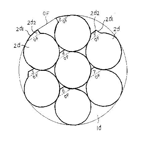
Fig. 6 is a schematic plan view concerning a fourth embodiment similar to the
third embodiment according to the present invention, showing a process of
manufacturing single-crystal semiconductor wafers of a 2-inch diameter from a
single-
- 14-
CA 02508733 2005-06-03
crystal semiconductor wafer having a 6-inch diameter. This process of
manufacturing
in the fourth embodiment can be carried out similarly as in the first
embodiment
described above.
Namely, in the fourth embodiment as well, there is initially grown a single-
crystal
compound semiconductor ingot of a 6-inch diameter (actually, the diameter is
slightly
larger than 6 inches for including a grinding allowance), and then its outer
periphery is
ground and an OF is formed thereon. This 6-inch diameter ingot is cut by a
dicer, a
multi-saw or the like, to provide a 6-inch diameter wafer 1 d. As shown in
Fig. 6, 6-
inch diameter wafer 1 d can then be cut by a laser similarly as in the first
embodiment to
provide seven 2-inch diameter wafers 2d.
In other words, similarly as in the third embodiment, a single process of
growing
a 6-inch diameter ingot and a single process of slicing the same can provide
seven times
as many 2-inch diameter wafers as the case of growing a 2-inch diameter ingot.
In the fourth embodiment shown in Fig. 6, on the other hand, each of 2-inch
diameter wafers 2d is cut out to have a protruding margin 2dl to be gripped
when
cleavage is carried out so as to form an OF. Many compound semiconductors have
significant cleavage characteristic along a crystal plane having a specific
low index.
Therefore, such cleavage characteristic can be utilized to form a presice OF
conveniently
and easily. In doing so, there has conventionally been made a wafer having a
diameter
larger than a target diameter in order to provide a margin to be gripped when
cleavage is
carried out. According to the fourth embodiment, however, there can be
obtained a
significant advantage that a wafer having a diameter larger than the target
diameter need
not be prepared even if cleavage is carried out to form an OF.
Furthermore, in the fourth embodiment, protruding margin 2d1 can be provided
with an identification mark 2d2, which can be used to identify each other a
plurality of
small-scale wafers 2d cut out from single large-scale wafer 1 d. For example,
therefore,
it is possible to determine that each of small-scale wafers 2d has been cut
out from what
part of large-scale wafer 1 d. For identification mark Zd2, a number may be
written in
-15-
CA 02508733 2005-06-03
protruding margin Zd 1 by using a laser beam used in laser cutting.
Alternatively, a
different number of dots or any other distinguishable marks may be provided
thereto.
Generally, it is more difficult to grow a large-scale single-crystal ingot
than to
grow a small-scale single-crystal ingot, because various defects including
twin crystals,
polycrystals, crystal slips and others are more likely to be caused in growing
a large-
scale ingot than a small-scale one. Conventionally, a large-scale wafer cut
out from an
ingot's part having such a defect cannot be shipped as a product and goes to
waste.
Furthermore, when a chip or a crack occurs in slicing off a large-scale single-
crystal
wafer by a dicer or a mufti-saw, the entire wafer cannot be shipped as a
product and
goes to waste. However, with a method of manufacturing small-scale single-
crystal
semiconductor wafers according to the present invention described above, there
can be
obtained a significant advantage that a large-scale wafer including a defects)
can be cut
into small-scale wafers, among which those having been cut out from non-
defective
ports can be shipped as products.
In the aforementioned embodiments, although a laser cutting method is
described
as a method of cutting out small-scale wafers from a large-scale wafer, it is
also possible
to use a well-known electric discharge machining method. In doing so, there
can be
used a thin-walled cylindrical discharging electrode having a peripheral shape
corresponding to the shape of a small-scale wafer to be cut out. In addition
to these
cutting methods, it is further possible to use a well-known wire saw method,
an
ultrasonic method, and a grinding method by means of a cylindrical core on
which
diamond is electrically Furthermore, of course, a plurality of large-scale
wafers may be
stacked for cutting simultaneously into small-scale wafers as long as the
stack can be cut.
Although a large-scale compound semiconductor wafer to be cut has a 6-inch
diameter at most at present, it goes without saying that the present invention
can be
applied to a larger wafer having an 8-inch or 12-inch diameter which will be
manufactured in the future. Similarly, although small-scale wafers cut out
have a 2-
inch diameter in the aforementioned embodiments, it goes without saying that
the
-16-
CA 02508733 2005-06-03
present invention can be used even in the case that a large-scale wafer to be
manufactured in the future is cut into small-scale wafers having a diameter of
3 inches
ore more (for example, a 9-inch diameter wafer can be cut to provide seven 3-
inch
wafers). Moreover, in the present invention, small-scale wafers cut out from a
large-
scale wafer are not required to have the same diameter. For example, it is
also possible
to cut a single large-scale wafer to provide a small-scale wafers) of a 2-inch
diameter
and ones) of a 3-inch diameter simultaneously.
Furthermore, the present invention is not limited to the wafer of the compound
semiconductor such as GaAs or InP described above, and can naturally be
applied to any
other compound semiconductor wafer such as GaN.
Industrial Applicability
As described above, according to the present invention, there can be provided
a
method of efficiently manufacturing single-crystal semiconductor wafers of a
relatively
small diameter from a single-crystal semiconductor ingot of a relatively large
diameter at
low costs, and a laser machining apparatus which can be used therefor. In
particular, it
is possible to provide still-highly-demanded compound semiconductor wafers of
a
relatively small diameter with high productivity and at low costs.
-17-