Note: Descriptions are shown in the official language in which they were submitted.
CA 02509785 2005-06-10
DESCRIPTION
Light Emitting Apparatus
Technical Field
The present invention relates to light emitting apparatuses and more
particularly
to light emitting apparatuses formed from nitride semiconductors. A light
emitting
apparatus of the present invention refers to a semiconductor device or
semiconductor
chip mainly constituted by a nitride semiconductor substrate and semiconductor
layers
laminated thereon in some cases and also refers to a device including a
semiconductor
chip mounted on a mounting component and sealed with resin in some cases.
Also, it
may refer to the both in some cases. Further, a semiconductor chip is called a
chip in
some cases. Further, a substrate and epitaxial layers formed thereon in a chip
are
simply called a substrate in some cases.
Background Art
Currently, white light emitting diodes (LEDs) have been widely employed for
illumination of compact electronic equipment such as portable information
terminals and
have the potentiality to be utilized for illumination for larger spaces or
larger areas in the
future. In order to utilize LEDs for illumination for larger spaces or larger
areas, it is
required to increase the light outputs of LEDs. Therefore, there is a need to
enable
flowing large currents through the electrodes of LEDs and overcome a problem
of
temperature increases caused by heat generation.
Fig. 59 illustrates the construction of a GaN-based LED which has been
currently proposed (a patent document 1 ). In this GaN-based LED, an n-type
GaN
layer 102 is provided on a sapphire substrate 101 and a quantum-well
construction 103
is formed between n-type GaN layer 102 and a p-type GaN layer 104. Light
emission
occurs at quantum-well construction 103. On p-type GaN layer 104, a p-
electrode 105
-1-
CA 02509785 2005-06-10
is formed to be in ohmic contact and on n-type GaN layer 102 an n-electrode
106 is
formed to be in ohmic contact.
These p-electrode 105 and n-electrode 106 are connected to a mounting
component 109 through solder balls 107, 108. The mounting component (sub-mount
component) is formed from an Si substrate and provided with circuits for
protection
against surge voltages from the outside. Namely, in order to prevent large
forward
voltages or reverse voltages from being applied to the light emitting
apparatus, the
electrical power branching circuit for protecting the light emitting apparatus
is
constituted by Zener diodes, etc., placing emphasis on that main factors of
circuit failure
for semiconductor of a nitride of Ga, Al, In or other group III element are
surge
voltages such as transient voltage and static discharge. Protection against
surge
voltages will be described in detail later.
The above GaN-based LED is characterized in that (al) p-type GaN layer 104 is
down-mounted and (a2) n-electrode layer 106 is formed on n-type GaN layer 102
so
that light is emitted from the backside of sapphire substrate 101. The
construction of
the GaN-based LED is significantly complicated as can be seen in Fig. 59. The
reason
that (a2) the n-electrode layer is formed on n-type GaN layer 102, which is
the cause of
such a complicated construction, is that sapphire substrate 101 is an
insulator and the n-
electrode can not be provided on the sapphire substrate.
As well as the above light emitting apparatus employing a sapphire substrate,
there has been often suggested that circuits for protection against transient
voltages and
static discharge are provided in light emitting apparatuses employing GaAs-
based, GaP-
based, or GaN-based compound semiconductors for use in light emitting
apparatus (see
patent documents 2-4). Particularly, in the case of GaN-based compound
semiconductors, the breakdown strengths in the reverse direction are about 50
V and
thus are low, and also the breakdown strengths for the forward voltage are
only about
150 V. Therefore, there has been importance attached to providing an
electrical power
branching circuit for the above protection. Namely, the above GaN-based chip,
etc., is
_2_
CA 02509785 2005-06-10
formed on the Si substrate of the sub-mount and on the Si substrate the
protection
circuit including Zener diodes is constituted. It can be said that suggestions
of many
protection circuits as above are the proof of that main factors of circuit
failure for
semiconductor of a nitride of Ga, Al, In or other group III element are surge
voltages
such as transient voltage and static discharge.
Besides the light emitting apparatus provided with the above protection
circuits,
there have been known examples of forming a GaN-based light emitting apparatus
on a
conductive SiC substrate. Namely, LEDs constructed to emit light from a p-type
GaN
layer using a laminate construction of (n-electrode on the SiC substrate
backside/SiC
substrate/n-type GaN layer/quantum-well laminate construction (light emitting
layer)/p-
type GaN layer/p-electrode) have been also widely utilized.
Patent Document 1: Japanese Patent Laying-Open No. 2003-8083
Patent Document 2: 3apanese Patent Laying-Open No. 2000-286457
Patent Document 3: Japanese Patent Laying-Open No. 11-54801
Patent Document 4: Japanese Patent Laying-Open No. 11-220176
Disclosure of the Invention
Problems to be Solved by the Invention
In the case of GaN-based LEDs using a sapphire substrate illustrated in Fig.
59,
the construction is complicated and the fabrication cast will be
unavoidablyincreased.
In order to develop the demand in large space illumination applications, LEDs
are
required to be cheap, and thus the aforementioned construction is not
desirable.
Furthermore, since p-electrode 105 and n-electrode 106 are placed on the down-
mounted surface side, the areas of the electrodes, particularly the area of
the p-electrode,
is restricted. In order to enable flowing large currents to achieve high
outputs, it is
desired that the p-electrode has particularly a larger area. However, with the
construction illustrated in Fig. 59, the area of the p-electrode is restricted
and
accordingly the light output is restricted. Further, in discharging heat
generated in
-3-
CA 02509785 2005-06-10
association with currents, providing two electrodes on one side is not
desirable.
Furthermore, there is large resistance to currents flowing in the direction
parallel
to the substrate through n-type GaN layer 102, which causes heat generation
and an
increase of the driving voltage and, therefore, an increase of the power
consumption.
Particularly, if the thickness of the n-type GaN layer is reduced in order to
shorten the
film forming processes, the yield of exposure of the n-type GaN film will be
significantly
degraded, besides the above problem of heat generation and power consumption
increases.
Further, as can be said in general for light emitting devices including the
above
light emitting device employing a sapphire substrate, since the heat radiating
area is
restricted and also the heat resistance (temperature increase caused by unit
introduced
energy per unit area) is large, the injection current per light emitting
apparatus can not
be increased. Particularly, in the case of using a sapphire substrate, since
the area of
the p-electrode is restricted, it is common to heat-design the apparatus with
little margin.
Further, in the case of GaN-based LEDs using a sapphire substrate, since the
heat radiating area is restricted, in order to reduce the electrical
resistance as much as
possible to reduce heat generation, it becomes necessary to employ a
construction in
which the p-electrode and the n-electrode are complicated in a comb shape to
widen the
contact area. Processing of such a comb-shaped electrode is not easy and the
fabrication cost will be certainly increased.
As previously described, the design of heat conditions is basically important
for
light emitting apparatuses and when an attempt is made to obtain high outputs,
there will
be restriction due to heat conditions as above. Therefore, in order to
alleviate this as
much as possible, a complicated electrode shape must be employed.
Further, there are the following problems. In the case where a GaN-based light
emitting apparatus formed on a sapphire substrate is down-mounted so that the
back
side of the sapphire substrate forms the light emitting surface, light with an
incident
angle greater than a predetermined angle experiences total internal reflection
at the
-4-
CA 02509785 2005-06-10
interface between the GaN layers which generate and propagate light and the
sapphire
substrate, and thus the light will not be emitted to the outside, since the
refractive index
of sapphire is about 1.8 and the refractive index of GaN is about 2.4. Namely,
lights
with incident angles 8 >_ sin 1 (1.8/2.4) ~ 4.2° will remain within the
GaN layers and will
not be emitted to the outside. Consequently, the light emission efficiency at
the main
surface of the sapphire substrate will be degraded. Although the problem of
the light
emission efficiency is important, there are still other problems. The light
experienced
the above total internal reflection propagates through the GaN layers and is
emitted
from the side portions of the GaN layers. Since the ratio of the light which
experiences
the above total internal reflection is significantly large and also the GaN
layers are thin,
the energy density of light emitted from the side portions becomes large. The
sealing
resin placed at the side portions of the GaN layers and irradiated with the
light is
damaged and this causes a problem of shortening the life of the light emitting
apparatus.
In the case of a GaN-based LED having a construction of (SiC substrate
backside n-electrode/SiC substrate/n-type GaN layer/quantum-well laminate
construction (light emitting layer)/ p-type GaN layer/ p-electrode) for
extracting light
from the p-layers side, the light absorption ratio at the p-electrode is large
and thus high
light outputs can not be emitted to the outside efficiently. When an attempt
is made to
reduce the coverage ratio of the p-electrode and namely increase the opening
ratio to
increase the amount of light emission, currents can not be flowed through the
entire p-
type GaN layer because of the high electrical resistance of the p-type GaN
layer.
Consequently, light emission can not be activated through the entire quantum-
well
construction, and thus the light emission output is decreased. Further, the
electrical
resistance will be increased and this will induce a problem of heat generation
and power
supply capacity. Also, if the thickness of the p-type GaN layer is increased
in order to
flow currents uniformly through the entire p-type GaN layer, the light
absorption at the
p-type GaN layer becomes large and the output will be restricted.
Means for Solving the Problems
-5-
CA 02509785 2005-06-10
It is an object of the present invention to provide light emitting apparatuses
which have simple constructions and thus can be fabricated easily, and can
stably
provide high light emission efficiencies for a long time period.
A light emitting apparatus according to the present invention is a light
emitting
apparatus including a nitride semiconductor substrate, an n-type nitride
semiconductor
layer at a first main surface side of the nitride semiconductor substrate, a p-
type nitride
semiconductor layer placed more distantly from the nitride semiconductor
substrate than
the n-type nitride semiconductor layer at the first main surface side and a
light emitting
layer placed between the n-type nitride semiconductor layer and the p-type
nitride
semiconductor layer at the first main surface side. In this light emitting
apparatus, the
nitride semiconductor substrate has a resistivity of 0.5 S2~cm or less and the
p-type
nitride semiconductor layer side is down-mounted so that light is emitted from
the
second main surface of the nitride semiconductor substrate at the opposite
side from the
first main surface.
With this construction, the n-type electrode is provided on the backside
(second
main surface) of the nitride semiconductor substrate with a low electrical
resistance.
Therefore, even when the n-electrode is provided with a low coverage ratio or
high
opening ratio, currents can be flowed through the entire nitride semiconductor
substrate.
Thus, the light absorption ratio at the emitting surface becomes lower and the
light
emission efficiency may be increased. Further, it goes without saying that
light
emission may occur at the side surfaces as well as at the second main surface.
The
same holds for the following light emitting apparatuses.
Further, the p-type nitride semiconductor layer side having a high electrical
resistance does not form a light emitting surface and therefore the p-type
electrode layer
may be formed on the entire surface of the p-type nitride semiconductor layer.
This
construction is advantageous in flowing large currents and suppressing heat
generation
and in discharging generated heat by conduction. Namely, restrictions caused
by heat
requirements may be drastically alleviated. Thus, there is no need to form a
comb-
-6-
CA 02509785 2005-06-10
shaped electrode in which the n-electrode and the p-electrode are complicated
in order
to reduce the electrical resistance.
Since the GaN substrate has an excellent conductivity, there is no need to
provide a protection circuit against surge voltages and the breakdown strength
may be
made significantly higher.
Further, complicated process steps are not performed and the fabrication cost
may be easily reduced.
Further, the nitride semiconductor "substrate" refers to a thick plate member
which may be independently portable and has a proper thickness and is
differentiated
from "films" or "layers" which are not independently and easily portable with
their
shapes kept. The same holds for a GaN substrate and A1N substrate which will
be
described later.
Another light emitting apparatus of the present invention is a light emitting
apparatus including a GaN substrate which is a nitride semiconductor
substrate, an n-
type AIXGaI_XN layer (x is in the range of from 0 to I) which is an n-type
nitride
semiconductor layer at a first main surface side of the GaN substrate, a p-
type AlxGai_xN
layer (x is in the range of from 0 to 1) placed more distantly from the GaN
substrate
than the n-type AIXGai_XN layer at the first main surface side, and a light
emitting layer
placed between the n-type AIXGaI_XN layer and the p-type AIXGaI_xN layer at
the first
main surface side. In this light emitting apparatus, the GaN substrate has a
dislocation
density of 108/cmz or less, and the p-type AIXGa~-xN layer side is down-
mounted so that
light is emitted from the second main surface of the nitride semiconductor
substrate at
the opposite side from the first main surface.
This construction is predicated on that the above GaN substrate of the present
invention has a conductivity and the electrical resistance may be easily
reduced. In
addition to the effects of the aforementioned light emitting apparatus, since
the GaN
substrate has a dislocation density of 108/cmz or less and the crystalinity is
high and also
the opening ratio is high, the light output from the second main surface may
be increased.
CA 02509785 2005-06-10
Further, light is emitted from the side surfaces.
Further, the continuousness of the refractive index is maintained and the
problem
of the aforementioned total internal reflection will not occur.
A further light emitting apparatus of the present invention is a light
emitting
apparatus including a conductive AIN substrate which is a nitride
semiconductor
substrate, an n-type AlxGa1_XN layer (0 <_ x < 1) which is an n-type nitride
semiconductor
layer at a first main surface side of the A1N substrate, a p-type AIXGaI_XN
layer (0 <_ x <_
1) placed more distantly from the AIN substrate than the n-type AIxGaI_XN
layer at the
first main surface side, and a light emitting layer placed between the n-type
AIXGa,_XN
layer and the p-type AIXGaI_xN layer at the first main surface side. The above
A1N
substrate has a heat conductivity of 100 W/(m~K) or higher, and the p-type
AlxGa1_XN
layer side is down-mounted so that light is emitted from the second main
surface of the
AlN substrate at the opposite side from the first main surface.
A1N has a significantly high heat conductivity and thus is excellent in heat
dissipation ability. Therefore, it is possible to suppress temperature
increases in the
light emitting apparatus by transferring heat from the above p-type AIxGaI_XN
layer to
the lead frame, etc. Further, the above A1N substrate also dissipates heat,
which
contributes to suppression of temperature increases. Further, this
construction is
predicated on that the AIN substrate is a conductive AIN substrate into which
impurities
have been implanted to provide a conductivity.
Brief Description of the Drawings
Fig. 1 is an illustration showing an LED of Inventive Example A according to a
first embodiment of the present invention;
Fig. 2 is an illustration showing the laminate construction including a light
emitting layer of the LED of Fig. 1;
Fig. 3 is an illustration showing the state of a wafer when taking chips of a
laminate construction out of the wafer;
_g_
CA 02509785 2005-06-10
Fig. 4 is an illustration showing the placement of the electrodes of Fig. 3;
Fig. 5 is an illustration showing Comparative Example B;
Fig. 6 is an illustration showing the laminate construction including a light
emitting layer of the LED of Comparative Example B;
Fig. 7 is an illustration showing the state of a wafer when taking chips
having the
laminate construction of Comparative Example B out of the wafer;
Fig. 8 is an illustration showing the placement of the electrodes of Fig. 7;
Fig. 9 is an illustration showing the relation between the applied current and
the
light output for Inventive Example A and Comparative Example B;
Fig. 10 is an illustration showing the relation between the current density in
the
light emitting layer and the light output for Inventive Example A and
Comparative
Example B;
Fig. 11 is an illustration showing an LED of Inventive Example C according to
a
second embodiment of the present invention;
Fig. 12 is an illustration showing an LED of Inventive Example C1 according to
the second embodiment of the present invention;
Fig. 13 is a plan view of the LED of Inventive Example C 1 of Fig. 12;
Fig. 14 is an illustration showing an LED of Comparative Example E;
Fig. 15 is a plan view of the LED of Comparative Example E of Fig. 14;
Fig. 16 is an illustration showing an LED of Inventive Example F according to
a
third embodiment of the present invention;
Fig. 17 is an illustration showing the placement of the electrodes when taking
chips having the laminate construction of Inventive Example F out of the
wafer;
Fig. 18 is an illustration schematically showing the current flows in an LED
chip
by calculation simulation;
Fig. 19 is an illustration schematically showing the current density ratio in
the
light emitting layer of the LED according to the third embodiment;
Fig. 20 is an illustration showing the applied current and the light output of
the
-9-
CA 02509785 2005-06-10
LED (no fluorescence material) according to the third embodiment;
Fig. 21 is an illustration showing the current density in the light output and
the
light output of the LED (no fluorescence material) according to the third
embodiment;
Fig. 22 is an illustration showing the relation between the applied current
and the
light output of the LED (including fluorescence material: white) according to
the third
embodiment;
Fig. 23 is an illustration showing the current density in the light emitting
layer
and the light output of the LED (including fluorescence material) according to
the third
embodiment;
Fig. 24 is an illustration showing Modification Example F-3 of the LED
according to the third embodiment;
Fig. 25 is an illustration showing the LED of Fig. 24;
Fig. 26 is an illustration showing the general outline of the transmittance
measurement test of the LED according to a fourth embodiment;
Fig. 27 is an illustration showing the state in which light passes through the
substrate in the transmittance measurement test illustrated in Fig. 26;
Fig. 28 is an illustration showing the influence of the thickness of the
substrate
on the transmittance;
Fig. 29 is an illustration showing the state after etching for device
separation in
order to take LEDs of Inventive Example L out of a wafer according to a fifth
embodiment;
Fig. 30 is an illustration showing the state when etching for device
separation in
order to take LEDs of Comparative Example M out of a wafer and forming an n-
electrode on the bottom of an etching slot according to the fifth embodiment;
Fig. 31 is an illustration showing the state when etching for device
separation in
order to take LEDs of Comparative Example N out of a wafer and forming an n-
electrode on the bottom of an etching slot according to the fifth embodiment;
Fig. 32 is an illustration showing an LED of Inventive Example Q according to
a
- 10-
CA 02509785 2005-06-10
seventh embodiment;
Fig. 33 is an illustration showing an LED of Inventive Example R according to
the seventh embodiment;
Fig. 34 is an illustration showing an LED of Inventive Examples S and T
according to an eighth embodiment;
Fig. 3 S is an illustration showing an LED of Inventive Example U according to
the eighth embodiment;
Fig. 36 is an illustration showing an LED of Inventive Example W according to
the eighth embodiment;
Fig. 37 is an illustration showing the influence of the oxygen concentration
on
the resistivity of the GaN substrate according to a ninth embodiment;
Fig. 38 is an illustration showing the influence of the oxygen concentration
on
the transmittance of the GaN substrate with respect to light (450 nm
wavelength)
according to the ninth embodiment;
Fig. 39 is an illustration showing the light outputs of light emitting devices
and
plan surface sizes in which currents flow uniformly, wherein the light
emitting devices
were fabricated from GaN substrates having varying thicknesses and oxygen
concentrations;
Fig. 40 is an illustration showing dislocation bundles in the GaN substrate
transferred to an epitaxial layer;
Fig. 41 is an illustration showing a dislocation bundle transferred to an
epitaxial
layer to be a hole-shape recess;
Fig. 42 is an illustration showing an ofd angle distribution with respect to
the c-
plane of a GaN substrate of 20 mm x 20 mm;
Fig. 43 is an illustration showing a construction in which a buffer layer is
placed
between the GaN substrate and the AIGaN clad layer according to an eleventh
embodiment;
Fig. 44 is an illustration showing the results of widening the ofl=angle range
-11-
CA 02509785 2005-06-10
which allows generating an light output of 8 mW or more;
Fig. 45 is an illustration showing a light emitting device according to a
twelfth
embodiment;
Fig. 46 is a cross sectional view focused on the p-electrode of the light
emitting
device according to a thirteenth embodiment;
Fig. 47 is a plan view of the penetratively viewed p-electrode of the light
emitting device according to the thirteenth embodiment;
Fig. 48 is an illustration showing the light emission and reflection of
Inventive
Example SS according to the thirteenth embodiment;
Fig. 49 is an illustration showing the light emission and reflection of
Comparative Example T6 according to the thirteenth embodiment;
Fig. 50 is an illustration showing the light emission and reflection of
Inventive
Example A for comparison;
Fig. 51 is an illustration showing the main surface of a GaN substrate in
which
plate-shape crystal inversion domains appear in a lattice shape in a
fourteenth
embodiment of the present invention;
Fig. 52 is cross sectional view of the GaN substrate illustrating the plate-
shape
crystal inversion domain of Fig. 51;
Fig. 53 is cross sectional view illustrating Inventive Example S6 of the
fourteenth embodiment of the present invention;
Fig. 54 is a plan view illustrating plate-shape crystal inversion domains in a
parallel placement different from Fig. 51, which is included in the fourteenth
embodiment of the present invention;
Fig. 55 is cross sectional view ofFig. 54;
Fig. 56 is a cross sectional view showing the light emission and reflection of
Inventive Example S7 according to a fifteenth embodiment;
Fig. 57 is a cross sectional view showing the light emission and reflection of
Inventive Example S8, which is another embodiment of the fifteenth embodiment;
-12-
CA 02509785 2005-06-10
Fig. 58 is a cross sectional view showing the light emission and reflection of
Comparative Example T7 according to the fifteenth embodiment; and
Fig. 59 is an illustration showing a conventional LED.
Description of Reference Characters
1: GaN substrate, 1 a: light emitting surface (second main surface), 2: n-type
GaN layer, 3: n-type AlxGai_xN layer, 4: MQW (light emitting layer), 5: p-type
AlXGa1_
XN layer, 6: p-type GaN layer, 11: n-electrode, 12: p-electrode, 12a: Ni/Au p-
electrode
in discrete arrangement, 13 : wire, 14: conductive adhesive, 15: epoxy resin,
21 a: mount
portion of lead frame, 21b: lead portion of lead frame, 25: device separation
slot, 25a:
bottom of device separation slot, 26: fluorescence material, 35: high
reflective film, 50:
chip boundary, L1: side length of p-electrode, L2: spacing of scribed lines
(side length of
chip), L3 : width of device separation slot, L4: side length of etched slot,
D: diameter of
n-electrode, r: distance from the center of light emitting layer, t: thickness
of n-type
GaN layer, 31: n-type AIGaN buffer layer, 32: p-type InGaN layer, 33 : Ag
electrode
layer, 46: fluorescence plate, 46a: surface of fluorescence plate with
projections and
depressions, 51: plate-shape crystal inversion domain, 52: trench, 61: bundle
(hole-
shaped recess), Rl: area having off angle of 0.05°, R2: area having off
angle of 1.44°.
Best Modes for Carrying Out the Invention
Either GaN substrates with a dislocation density equal to or less than 10g/cm2
or
A1N substrates with a thermal conductivity equal to or higher than 100 W/
(m~K) satisfy
the condition of the above nitride semiconductor substrate that the
resistivity is equal to
or lower than 0.5 S2~cm. The selective embodiments of the light emitting
device of the
present invention including the aforementioned nitride semiconductor
substrates are
applicable as other selective embodiments of the light emitting devices of the
present
invention employing a GaN substrate or an A1N substrate as the semiconductor
substrate by employing, as the substrate, a GaN substrate or an AIN substrate,
which are
one of nitride semiconductor substrate.
-13-
CA 02509785 2005-06-10
Then, embodiments of the present invention will be described using drawings.
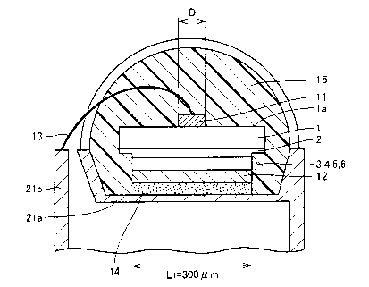
First Embodiment
First, a comparison will be made between a sapphire substrate and a GaN
substrate, which is a nitride semiconductor substrate. Fig. 1 is an
illustration showing
an LED of an Inventive Example A according to a first embodiment of the
present
invention. There has been formed a laminate construction including a light
emitting
layer, which will be described later, on a first main surface side of a GaN
substrate 1 and
a p-electrode 12 has been formed thereon. This embodiment has a characteristic
that
this p-electrode 12 is down-mounted to a lead frame mount portion 21 a with a
conductive adhesive 14.
A second main surface 1 a of GaN substrate 1 is the surface which emits light
generated at the light emitting layer and an n-electrode 11 is provided on
this surface.
This n-electrode 11 is formed not to cover the entire surface of the second
main surface.
It is important to make the ratio of the portion that has not been covered
with n-
electrode 11 larger. When the opening ratio is made larger, the amount of
light
shielded by the n-electrode will decrease and therefore the emission
efficiency of light
emitted outside will be increased.
N-electrode 11 is electrically connected to a lead portion 21b of a lead frame
through a wire 13. Wire 13 and the aforementioned laminate construction are
sealed
with an epoxy resin 15. The laminate construction from GaN substrate 1 to p-
electrode 12, of the aforementioned construction, is enlarged in Fig. 2. In
Fig. 2, the
laminate construction of Fig. 1 is shown upside down.
Referring to Fig. 2, an n-type GaN epitaxial layer 2 is placed on GaN
substrate 1
and an n-type AlXGa1_XN layer 3 is formed thereon. Further, there is formed
thereon a
quantum well (MQW) 4 consisting of AIXGaI_xN layers and AIXInyGa1_X_yN layers.
A p-
type AIXGaI_XN layer 5 is placed such that quantum well 4 is sandwiched by p-
type
AlXGa1_XN layer 5 and n-type AIXGa~_XN layer 3, and a p-type GaN layer 6 is
placed
thereon. In the aforementioned construction, quantum well 4 causes light
emission.
-14-
CA 02509785 2005-06-10
Further, as illustrated in Fig. l, a p-electrode 12 is formed to cover the
entire surface of
p-type GaN layer 6 and is down-mounted. Next, a fabricating method of the LED
of
Inventive Example A will be described.
(al) A GaN ofd substrate angled by 0.5° with respect to the c-plane was
employed. This substrate has a resistivity of 0.01 SZ~cm, a dislocation
density of
lE7/cmz and a thickness of 400 Vim.
(a2) The following laminate construction was fabricated on the Ga surface,
which is a first surface, of the GaN substrate by MOCVD (Metal Organic
Chemical
Vapor Deposition). (Si-doped n-type GaN layer la Si-doped n-type AIo,ZGao.sN
layer
being a clad layer/MQW (Multi-Quantum Well) which consists of three layers,
each
being a two-layers construction comprised of a GaN layer and an Ino.lsGao.ssN
layer/a
Mg-doped p-type AIo.2Ga~.gN layer being a clad layer/a Mg-doped p-type GaN
layer).
(a3) The light emission wavelength was 450 nm and the internal quantum
efEciency was 50%, which was calculated by, for convenience, comparing the PL
(Photo Luminescence) intensity at the low temperature 4.2 K and the PL
intensity at a
room temperature of 298 K.
(a4) This wafer was activated to lower the resistance of the Mg-doped p-type
layer. The Mg-doped p-type AIGaN layer and the Mg-doped p-type GaN layer had
carrier concentrations of SE17/cm3 and 1E18/cm3, respectively, which were
determined
by hall measurement.
(a5) This wafer was etched by photolithography technique and RIE (Reactive
Ion Etching) from the Mg-doped p-type layers side to the Si-doped n-type
layers. By
this etching, device separation slots 25 were formed to achieve device
separation as
illustrated in Fig. 3. The device separation slot had a width L3 of 100 Vim.
(a6) On the N-surface at the back side of the GaN substrate, which was the
second main surface, n-electrodes with a diameter(D) of 100 ~m were formed at
the
centers of the chips with a pitch of 400 p.m by photolithography technique,
vapor
deposition and lift-off method (see Figs. 3 and 4). As the n-electrodes, a
laminate
-15-
CA 02509785 2005-06-10
construction consisting, from the bottom side, of (a Ti layer 20 nm/an Al
layer 100 nm/a
Ti layer 20 nm/an Au layer 200 nm) was formed in contact with the GaN
substrate.
This was heated in the atmosphere of nitrogen (NZ) to lower the contact
resistance to
below lE-5 S2~cm2.
(a7) As the p-electrode, an Ni layer with a thickness of 4 nm was formed in
contact with the p-type GaN layer and an Au layer with a thickness of 4 nm is
formed on
the entire surface thereof (see Figs. 3 and 4). This was heat-treated in the
atmosphere
of inert gas to change the contact resistance to SE-4 SZ~cm2.
(a8) Subsequently, as illustrated in Figs. 3 and 4, the above construction was
scribed to form chip boundaries 50 as the side walls. The chipped
constructions were
made to be light emitting devices. A chipped light emitting device had a light
emitting
surface with a shape of 300 pm square (a square with a side length of 300 p.m)
and had
a light emitting layer with a shape of 300 pm square. Namely, as illustrated
in Fig. 4,
Ll = 300 pm and L2 = 400 Vim. Further, the width L3 of the device separation
slot =
100 ~m and the diameter D of the n electrode = 100 pm.
(a9) Refernng to Fig. 1, the above chip was mounted on the mount portion 21a
of a lead frame such that the p-type GaN layer side of the above chip was in
contact
with the mount portion 21a to form a light emitting device. The light emitting
device
and the mount were secured to each other and conduction was established
therebetween
by a conductive adhesive 14 applied to the mount portion.
(a10) In order to facilitate heat radiation from the light emitting device,
the light
emitting device was mounted to the mount portion such that the entire surface
of the p-
type GaN layer of the light emitting device was in contact with the mount
portion.
Further, as the adhesive, an Ag-based adhesive with high heat conductivity was
selected,
and as the lead frame, a CuW-based lead frame with high conductivity was
selected.
Consequently, the resultant heat resistance was 8°C/W.
(al l) Further, conduction was established between the n-electrode and the
lead
portion of the lead frame by wire bonding, and then the light emitting device
was sealed
- 16-
CA 02509785 2005-06-10
with an epoxy resin to make the light emitting device to be a lamp.
Next, a Comparative Example B will be briefly described. In Fig. 5, a p-
electrode 112 is down-mounted on the lead frame mount portion by conductive
adhesive
114. Further, the n electrode is connected to a lead frame mount portion 121 a
separated from the lead mount portion to which the p-electrode is connected. A
laminate construction (Fig. 6) including a light emitting layer is formed
thereon and is
contacted with a predetermined area of n-type GaN layer 102. An n-type GaN
layer
102 is formed on a sapphire substrate 101 and an n-electrode 111 is formed on
the area
outside of the area with which the aforementioned laminate construction is
contacted.
The n-electrode 111 is electrically connected to a lead frame mount portion
121a or a
lead frame lead portion 121b through a wire or conductive adhesive.
Light emitted from the light emitting layer is emitted outside through
sapphire
substrate 101. An epoxy resin 115 is encapsulated to cover the aforementioned
laminate construction including the sapphire substrate.
(bl) A sapphire insulating off substrate angled by 0.2° with respect to
the c
plane was employed. The sapphire substrate had a thickness of 400 ~tm.
(b2) to (b4) The same processes as (a2) to (a4) in Inventive Example A were
applied to the sapphire substrate.
(b5) In the case of Comparative Example B, the sapphire substrate is an
insulator
and therefore the n-electrode must be formed on the grown-films side,
similarly to the p-
electrode. Therefore, this wafer was etched from the Mg-doped p-type layers
side to
the Si-doped n-type layers using Cl-based gas by photolithography technique
and RIE to
expose the n-type GaN layer for forming the n-electrode. Then, the same device
separation as that of Inventive Example A was performed (Figs. 7 and 8). The
shape
of the device was 300 ~m square and the exposed area of the n-type GaN layer
therein
was 150 ~m square per device. Namely, the square step of the exposed area had
a side
length L4 of 1 SO Vim.
(b6) On the exposed n-type GaN layer, an n-electrode with a diameter of 100
- 17-
CA 02509785 2005-06-10
p.m was formed by photolithography technique, vapor deposition, and lift-off
method.
The thickness, the heat treatment and the contact resistance were the same as
those of
Inventive Example A.
(b7) A p-electrode was placed on the p-type GaN layer in which the n-type
GaN exposed area 150 ~m square had been removed from the device of 300 pm
square.
The thickness, the heat treatment and the contact resistance were the same as
those of
Inventive Example A.
(b8), (b9) The same processes as the corresponding processes of Inventive
Example A were performed.
(b 10) Similarly to Inventive Example A, in order to facilitate the heat
radiation
from the light emitting device, the light emitting device was mounted on the
mount
portion such that the entire surface of the p-type GaN layer of the light
emitting device
was in contact therewith. In Fig. 5, the contact area between p-type GaN layer
106
and p-electrode 112 was set to 0.0675 mm2. The heat radiation of the light
emitting
device occurs in quantum layer 104 and p-type GaN layer 106 and therefore this
heat
radiation is mainly determined by the area of p-electrode 112. In the case of
Fig. 5, n-
electrode 111 is also connected to mount portion 121 a of the lead frame by
conductive
adhesive 114, but the heat radiation area is substantially the aforementioned
contact area
0.0675 mm2. In Inventive Example A, the contact area between p-type GaN layer
6
and p-electrode 12 was 0.09 mmz. The adhesive and the material of the lead
frame
were the same as those of the Inventive Example A. In Comparative Example B,
in
reflecting the aforementioned construction, the heat resistance was
10.4°C/W, which
was 1.3 times that of Inventive Example A, and therefore was degraded.
(bl 1) The same process as the corresponding process of Inventive Example A
was performed.
(Experiments and Results)
Inventive Example A and Comparative Example B were mounted within an
integrating sphere and then predetermined currents were applied to them. The
values
-18-
CA 02509785 2005-06-10
of output lights which were focused and output from a detector were compared.
The
result is shown in Fig. 9. In Fig. 9, under relatively ideal conditions where
currents are
injected without leaking and there are relatively little non-radiation
recombination and
low chip-temperature rise due to heat radiation, the light output value
increases in
proportion to the increase of the applied current. For example, for injection
of 20 mA,
Inventive Example A generated an output of 8 mW, while Comparative Example B
generated an output of 7.2 mW.
Inventive Example A was mainly constructed by a GaN epitaxial filmlGaN
substrate, while Comparative Example B was mainly constructed by a GaN
epitaxial
film/sapphire substrate. The sapphire substrate had a refractive index of
about 1.8, and
this was significantly smaller than the refractive index 2.4 of GaN.
Therefore, in
Comparative Example B, light was generated in the GaN epitaxial film and
propagated,
and than the light was prone to total internal reflection at the interface
between the GaN
epitaxial film and the sapphire substrate. For this reason, the output of
Comparative
Example B was lower than that of Inventive Example A.
However, when the current was increased five-fold and 100 mA was applied to
Inventive Example A and Comparative Example B, Inventive Example A generated
five
times the output, or 40 mA, while Comparative Example B generated only 25.2 mW
(see Fig. 9). At this time, the current density in the MQW light emitting
portion was
110 Alcm2 in Inventive Example A and 150 A/cm2 in Comparative Example B.
Namely, the current density in the MQW light emitting portion of Inventive
Example A
was larger than that of the Comparative Example B.
This means that in Inventive Example A the heat radiating area was
sufficiently
large for radiated heat and the n-electrode was provided on the second main
surface side
of the substrate so that there was no area in which the current density became
significantly large. On the other hand, in Comparative Example B the heat
radiating
area was smaller than that of Inventive Example A and fizrther the n-electrode
was
formed on the exposed n-type GaN layer, and therefore the current density of
the
-19-
CA 02509785 2005-06-10
current flowing through the n-type GaN layer in the direction parallel to the
layer
significantly increased. As a result, in the Comparative Example B, heat
radiation
furtherincreased.
Further, in Inventive Example A, unlike in Comparative Example B, the n-
electrode and the p-electrode are placed at opposite positions and therefore
there is no
possibility of electrical short-circuits. Therefore, it is possible to prevent
increases of
additional fabrication cost such as for providing a film for electrically
insulating between
the p-electrode and n-electrode for preventing electrical short-circuits in
Comparative
Example B in which the electrodes exist at the same side.
Further, test results about the electrostatic withstand voltages of Inventive
Example A and Comparative Example B will be described. The tests were
performed
by generating electric discharge between the light emitting device and an
electrostatically
charged condenser placed oppositely. At this time, Comparative Example B was
broken at an electrostatic voltage of about 100 V. On the other hand,
Inventive
Example A was not broken until about 8000 V. It was proven that Inventive
Example
A had an electrostatic withstand voltage which was 80 times that of
Comparative
Example B.
Further, in Inventive Example A, the GaN-based light emitting device is formed
on the GaN substrate. Therefore, even though the GaN-based light emitting chip
is
down-mounted so that light is emitted from the back side of the GaN substrate,
there is
no refractive index difference between them. Thus, light propagates from the
GaN-
based light emitting chip to the GaN substrate without experiencing total
internal
reflection. Therefore, as compared with constructions in which a sapphire
substrate is
employed to form a GaN-based light emitting device, the light output from the
GaN
substrate main surface may be increased. Further, there will be no extremely-
concentrated light emission from the sides of the GaN layer and therefore the
sealing
resin will not be subjected to damage. Thus, the life time will not be
restricted by the
sealing resin.
-20-
CA 02509785 2005-06-10
As the inventive example, there has been merely described an example of the
light emission wavelength 450 nm, and the same effects may be obtained by
different
light emission wavelengths and layer constructions. Also, it goes without
saying that
the equivalent effects may be obtained by employing an AIxGaI_XN substrate
(wherein x
is greater than 0 and is equal to or less than 1) instead of the GaN
substrate, provided
that the substrate has equivalent characteristics.
Second Embodiment
In a second embodiment of the present invention, Inventive Example C having an
increased area will be described. Inventive Example C has the same
construction as
that of Inventive Example A illustrated in Fig. 1. However, while the
dimension L1 is
0.3 mm (300 p,m) in Inventive Example A, L1 is 3 mm or tenth and therefore the
area is
100 times in Inventive Example C, as illustrated in Fig. 11. First, the
fabricating
method of Inventive Example C is as follows.
(Inventive Example C)
(cl) to (c5) The same processes as the corresponding processes of Inventive
Example A were performed, but a larger GaN substrate was employed.
(c6) On the second main surface at the back side of the GaN substrate, n-
electrodes with a diameter of 100 p.m are formed with a pitch of 3.1 mm by a
photolithography technique, vapor deposition and lift-off method. As the n
electrodes,
a laminate construction consisting, from the bottom side, of (a Ti layer 20
nm/an Al
layer 100 nmla Ti layer 20 nmlan Au layer 200 nm) was formed in contact with
the back
side of the above GaN substrate. This was heated in an inert atmosphere to
reduce the
contact resistance to below lE-5 S~,~cmz.
(c7) The same process as the corresponding process of Inventive Example A was
performed.
(c8) Subsequently, the construction was scribed to make it to be desired
shapes
and the chipped constructions were made to be light emitting devices. The
chipped
light emitting devices had a size of 3 mm square.
-21 -
CA 02509785 2005-06-10
(c9) to (cl 1) The same processes as the corresponding processes of Inventive
Example A were performed. Then, Modification Example C1 in which the placement
of the n-electrode is changed from that of Inventive Example C was fabricated
as
follows.
(Inventive Example C 1 )
Figs. 12 and 13 are illustrations showing Inventive Example C 1 which is an
modification of Inventive Example C. Inventive Example C1 is characterized in
that n-
electrodes 11 are placed at the four corners of the GaN substrate. Further,
for
mounting the semiconductor chip, a reflective cup 37 is placed in the lead
frame such
that it surrounds the semiconductor chip.
In fabricating Inventive Example C1, the same processes as the corresponding
processes of Inventive Example A were performed. However, four Au wires were
employed as the bonding wires and the diameter of the cross sections of the Au
wires
was 25 pm. Each of the electrodes placed at the four corners has a shape of 45
pm
square.
Then, Comparative Example D will be described. Comparative Example D has
the same construction as that illustrated in Fig. 5. However, LI was 300 ~m
(0.3 mm)
in Comparative Example B, L1 is 3 mm and thus tenth in Comparative Example D.
The size L4 of the portion of the n-type GaN layer for forming an n-electrode
is 150 Vim,
which is the same as that of Comparative Example B of Fig. 5. The fabrication
method
of Comparative Example D is as follows.
(Comparative Example D)
(dl) A larger insulating sapphire off substrate angled by 0.2° with
respect to the
c-plane was employed. This substrate had a thickness of 400 p.m.
(d2) to (d4) The same processes as the corresponding processes of Inventive
Example A were performed.
(d5) In Comparative Example D, the sapphire substrate is an insulator and
therefore the n electrode must be formed on the grown-films side similarly to
the p-
-22-
CA 02509785 2005-06-10
electrode. Therefore, this wafer was etched from the Mg-doped p-type layers
side to
the Si-doped n- type layers by photolithography technique and RIE using Cl-
based gas
to expose the n-type GaN layer for forming the n-electrode. Then, the same
device
separation as that in Inventive Example A of was performed. The device had a
size of
3 mm square and thus had a larger size. The dimension of the exposed area of
the n-
type GaN layer was 150 ~m square per device.
(d6) On the exposed n-type GaN substrate, n-electrodes with a diameter of 100
pm were formed by photolithography technique, vapor deposition and lift-off
method.
The thickness, the heat treatment and the contact resistance were the same as
those of
Inventive Example A.
(d7) P-electrodes were placed on the p-type GaN layer in which device
separation slots and the exposed areas of 150 ~m square of the n-type GaN
layer for
placing n-electrode had been removed from the device area of 3.1 mm square.
The
thickness, the heat treatment and the contact resistance were the same as
those of
Inventive Example A.
(d8) to (dl l) The same processes as the corresponding processes of Inventive
Example A were performed.
Substantially, Comparative Example E will be described. Comparative
Example E is the same as Comparative Examples B and D in that a sapphire
substrate is
employed and p-electrode 112 and n-electrode 111 are both formed on the down
mounting side as illustrated in Fig. 14. Comparative Example E is, however,
different
from them in that as clearly illustrated in the plan view in Fig. 15, p-
electrode 112 has a
comb-shape, n-electrodes 111 are placed between the teeth of the comb, and an
insulator is placed between p-electrode 112 and n-electrodes 111. This is
intended for
uniformizing the current flowing through the p-electrode and the n-electrode
to prevent
formation of areas in which the current density becomes extremely large. The
fabrication method of this Comparative Example E is as follows.
(Comparative Example E)
- 23 -
CA 02509785 2005-06-10
With the same fabrication method as that of Comparative Example D, as n-
electrodes 111, five comb electrodes with a width of 0.1 mm was formed with a
pitch of
0.5 mm (Figs. 14 and 15). The p-electrode was formed at the remaining area of
n-type
GaN layer 102 such that n-electrodes 111 and p-electrode 112 were spaced by
0.1 mm
from each other. Further, an insulator 119 for surface protection was formed
at the
gaps between the n-electrodes and the p-electrode in order to prevent the
respective
electrodes from being electrically short-circuited. Further, in order to
prevent short-
circuits, a conductive adhesive 114 was provided on the area of mount portion
121 a of
the lead frame which corresponded to the position of the respective
electrodes. The
chip was mounted to the lead frame while displacement of the chip and the lead
frame in
the lateral direction, the longitudinal direction and the rotation direction
were controlled.
(Experiments and Results)
Inventive Example C and Comparative Example D were mounted within an
integrating sphere and then predetermined currents were applied to them. The
values
of output lights which were focused and output from a detector were compared.
For
example, when a current of 20 mA was applied, Inventive Example C generated an
output of 8 mW, while Comparative Example D generated an output of 7.2 mW. On
the other hand, when a current of 2 A (2000 mA) was applied, Inventive Example
C
generated 100 times the output, namely 800 mW. However, Comparative Example C
was broken:
Therefore, under the condition where Comparative Example D was not sealed
with resin, electric currents were applied to Comparative Example D and the
temperature of the device was measured by a thermoviewer. As a result, it was
proven
that abnormal heat generation occurred at the area in which currents
intensively flowed
through the n-type GaN layer in the direction parallel to the layer from the n-
electrode
toward the MQW light emitting portion and consequently Comparative Example D
was
broken.
Thus, in contrast to Comparative Example D, there was fabricated a light
-24-
CA 02509785 2005-06-10
emitting device having a construction in which currents flowing through the n-
type GaN
layer in the direction parallel to the layer from the n-electrode toward the
MQW light
emitting portion were distributed. This was Comparative Example E. Comparative
Example E generated an output of 7.2 mW for an applied current of 20 mA, and
an
output of 720 mW for an applied current of Z A. Thus, Comparative Example E
generated outputs which were 0.9 time that of Inventive Example C.
Thus, in order to obtain performance near that of Inventive Example C,
significantly-complicated constructions and processes are required as compared
with
Inventive Example C, and therefore the fabrication cost increases.
Then, for Inventive Example C and Comparative Examples D and E,
electrostatic withstand voltage tests were performed. The tests were
performed, as
previously described, by generating electric discharge between the light
emitting device
and an electrostatically charged condenser placed oppositely. Then,
Comparative
Examples D and E were broken at an electrostatic voltage of 100 V. On the
other
hand, Inventive Example C was not broken until about 8000 V. Namely, the
inventive
example offered a significantly high electrostatic withstand voltage, which
was
approximately 80 times that of the comparative examples.
Inventive Example C 1 had an opening ratio much greater than 50% and almost
100%. Further, since n-electrodes are placed at the corners of the GaN
substrate, they
are much less prone to become obstruction of light emission, as compared with
the case
where they are placed at the center. As illustrated in Fig. 12, the n
electrodes are
placed outside of the active layer, in a plan view, the n electrodes will
never affect the
light emission. As a result, Inventive Example C 1 can achieve higher outputs
than
Inventive Example C.
Third Embodiment
In a third embodiment of the present invention, influences of the opening
ratio at
the light emitting surface and the electrical resistance of the GaN substrate
on the light
output were determined. The adjustment of the opening ratio was performed by
-25-
CA 02509785 2005-06-10
varying the substrate area, the p-electrode size and the n-electrode size. As
a test
sample, an LED having the construction illustrated in Fig. 1 was employed.
However,
some of the tests were performed for a test sample provided with a
fluorescence
material 26 to be formed as a white LED as illustrated in Fig. 16. The test
samples
were three samples, namely Inventive Example F and Comparative Examples G, H
each
including a GaN substrate having a resistivity deviated from the range of the
present
invention. For each sample F, G and H, an LED including no fluorescence
material and
sealed with epoxy resin as illustrated in Fig. 1 and a white LED equipped with
a
fluorescence material illustrated in Fig. 16 were fabricated. The opening
ratio was
defined as follows: {(area of p-electrode - area of n-electrode/area of p-
electrode} x
100 (%).
In Inventive Example F, Ll = 8 mm, D = 100 p.m, and the opening ratio is
almost 100%. Also, in Comparative Example G, L1 = 0.49 mm, D = 100 ~m and the
opening ratio is 97%. In Comparative Example H, L1 = 8 mm, D = 7.51 mm and the
opening ratio is 31%. The fabrication methods of the aforementioned Inventive
Example F, Comparative Examples G and H will be described.
(Inventive Example F)
(fl ) to (f5) The same processes as the corresponding processes of Inventive
Example A were performed.
(f6) Subsequently, as illustrated in Fig. 17, the construction was scribed to
be
desired shapes and the chip-shaped constructions formed light emitting
devices. The
resultant light emitting devices had a size of 8 mm square.
(f7) to (fl 1) The same processes as the corresponding processes of Inventive
Example A were performed.
(fl2) In addition to the above (fl 1), a white-emitting lamp was fabricated by
mounting a fluorescence material on the n-electrode side of the light emitting
device
which had been mounted on the mount of the lead frame in (fl 0) and then
sealing the
light emitting device with an epoxy resin. For this, a fluorescence material
which
-26-
CA 02509785 2005-06-10
generated I 80 lm for 1 watt of light output with 450 nm was employed.
(Comparative Example G)
(gl) An n-type GaN off substrate angled by 0.5° with respect to the c-
plane was
employed. A GaN ofd substrate having a resistivity of 0.6 SZ~cm, which was
higher
than the range of the present invention of 0.5 S2~cm or less, was selected.
The GaN
substrate had a dislocation density of lE7/cm2 and a thickness of 400 p.m.
(g2) to (g5) The same processes as the corresponding processes of Inventive
Example A were performed.
(g6) Subsequently, the construction was scribed into desired shapes and the
chipped constructions formed light emitting devices. The resultant light
emitting
device had a size of 0.49 mm square.
(g7) to (g12) The same processes as the corresponding processes of Inventive
Example F were performed.
(Comparative Example H)
(hl) An n-type GaN ofd substrate angled by 0.5° with respect to the c-
plane was
employed. A GaN ofI=substrate having a resistivity of 0.6 S2~cm, which was
higher
than the range of the present invention of 0.5 S2~cm or less, was selected.
The GaN
substrate had a dislocation density of lE7/cmz and a thickness of 400 p.m.
(h2) to (h5) The same processes as the corresponding processes of Inventive
Example F were performed.
(h6) Subsequently, the construction was scribed into a desired shape and the
chipped constructions formed light emitting devices. The resultant light
emitting
device had a size of 8 mm square.
(h7) to (hl2) The same processes as the corresponding processes of Inventive
Example F were performed.
(Experiments and Results)
(1) For Inventive Example F and Comparative Examples G and H, the current
distribution in the area in which currents spread relatively uniformly from
the n-electrode
-27-
CA 02509785 2005-06-10
toward the MQW layer was calculated by simulations. The results of the
simulations
were reflected on the device designs of Inventive Example F and Comparative
Examples
G and H. Fig. 18 illustrates a conceptual illustration of the spread of
currents. Fig.
19 is an illustration showing the current density ratio at the distance r,
wherein r is the
radial distance from the center of the MQW light emitting layer 4. The current
density
at the center of the n-electrode is defined as I . (i) The result of Inventive
Example F:
the current density was at a maximum directly under the n-electrode and
decreased with
increasing distance from the n-electrode. Also, the range in which the current
density
exceeded 1/3 of that directly under the n-electrode was a range with a
diameter of 12
mm centered directly under the n-electrode. Based on the result, the size of
the light
emitting device was set to 8 mm square which was included therein. On the N-
surface,
which was the second main surface, of the GaN substrate, n electrodes with a
diameter
of 100 ~.m were formed at the centers of chips with a pitch of 8.1 mm by
photolithography technique, vapor deposition and lift-off method. In this
case, the
ratio of the area of the N-surface of the GaN substrate at which no n-
electrode existed,
namely the opening ratio, was substantially 100% per device. The thickness,
the heat
treatment and the contact resistance were the same as those of Inventive
Example A.
(ii) The result of Inventive Example G: the range in which the current density
exceeded
1 /3 of that directly under the n-electrode was a range with a diameter of 0.7
mm
centered directly under the n-electrode. Therefore, the diameter of the n-
electrode was
set to 100 ~tm in agreement with Inventive Example E, and the chip size was
set to 0.49
mm square, which was included in the diameter of 0.7 mm. On the N-surface of
the
GaN substrate, n-electrodes with a diameter of 100 ~m was formed at the
centers of
chips with a pitch of 0.5 mm by photolithography technique, vapor deposition
and lift-
off method. In this case, the opening ratio was about 97% per device. The
thickness,
the heat treatment and the contact resistance were the same as those of
Inventive
Examples A to E. (iii) In Comparative Example H, the chip size was set to 8 mm
square in agreement with Inventive Example E. The GaN substrate had the same
- 28 -
CA 02509785 2005-06-10
electrical resistivity as that of Comparative Example G and the diameter of
the spread of
currents would be 0.7 mm. Therefore, in order to flow currents through the 8
mm
square uniformly (I/3 or more of the current density directly under the n-
electrode), the
n-electrode was required to have a diameter of 7. S 1 mm. Thus, on the second
main
surface (light emitting surface), n-electrodes with a diameter of 7.51 mm were
formed
with a pitch of 8.1 mm by photolithography technique, vapor deposition and
lift-off
method and the width of the scribing was set to 0. I mm. In this case, the
opening ratio
was about 31% per device.
(2) Inventive Example F and Comparative Examples G and H equipped with no
fluorescence material were mounted within an integrating sphere and then
predetermined
currents were applied to them. The values of output lights which were focused
and
then output from a detector were compared. The results are shown in Figs. 20
and 21.
When applying a current of 20 mA, Inventive Example F and Comparative
Examples G and H generated outputs of 8 mW, 7.8 mW and 2.5 mW respectively,
which were consistent with the area ratio of the area at which the electrode
was not
formed. Inventive Example F generated the highest light output. Comparative
Example G generated a light output which was not high as that of Inventive
Example F,
but relatively high. Then, when 500 times the current, or 10 A, was applied to
them,
Inventive Example F and Comparative Example H generated outputs of 4 mW and
1.3
mW respectively, which were consistent with the area in which the electrode
was not
formed.
The output of Comparative Example G increased in proportion to the applied
current to 0.1 W at an applied current of 0.26 A and thus at a current density
in the light
emitting portion of 110 A/cm2. However, from then on, the output reached
saturation
with increasing temperature caused by heat generation and Comparative Example
G was
broken by an applied current of 10 A.
Figs. 22 and 23 illustrate the results of luminance measurements for the
aforementioned three types of test samples. Fig. 22 is an illustration showing
the
-29-
CA 02509785 2005-06-10
relation between the applied current and the resultant luminance for the white-
emitting
LEDs equipped with a fluorescence material. Fig. 23 is similarly an
illustration
showing the relation between the current and the luminance. The same
fluorescence
material was employed in Inventive Example F and Comparative Example H, but
the
luminance varied depending on the area ratio of the area at which the
electrode was not
placed. Thus, when the applied current was 10 A, the luminances of Inventive
Example F and Comparative Example H were 720 lm/chip and 234 lm/chip
respectively.
The Comparative Example had a thermal limit of 18 Im/chip at an applied
current of
0.26 A and was broken by an applied current of 10A. According to Figs. 22 and
23,
only Inventive Example F generated high luminances at high currents.
Further, in the present embodiment, the applied current is 10 mA at a maximum
since if the current is increased above that, then the Joule heat density at
the n-electrode
will become excessive and consequently significant heat generation will occur.
By increasing the size of the n-electrode or by sufficiently reducing the
contact
resistance, the same effects may be achieved for currents up to a maximum
current of 70
A, which is corresponding to an current density of 110 A/cm2.
(Inventive Examples F-2 and F-3)
The same processes as those of the Inventive Example F were performed. In
Inventive Example F-2, an n-electrode with a diameter D of I mm (an area of
0.785
mmz) was placed at the center of a GaN substrate. In Inventive Example F-3, n-
electrodes of 450 p.m square were placed at the four corners of a GaN
substrate (Figs.
24 and 25). As illustrated in Fig. 24 and Fig. 25, the n-electrodes placed at
the four
corners were each electrically connected to the lead frame by bonding wires.
The
bonding wires were Au wires and had a cross section with a diameter of 300
p.m. In
this case, both the examples had an opening ratio of about 100%. Further,
similarly to
Inventive Example C1, a reflection cup 37 which was a cup-shaped reflective
body was
placed.
Similarly to Inventive Example F, the example having no fluorescence material
-30-
CA 02509785 2005-06-10
was mounted within an integrating sphere and then predetermined currents were
applied
to them to cause light emission. The value of output light which was focused
and
output from a detector was measured. An output of 8 mW was generated for an
applied current of 20 mA, and an output of 4 W was generated for an applied
current of
500 times the current or 10 A. An output of 28 W was generated for an applied
current of 70 A.
Further, in the case of a while-emitting LED provided with a fluorescence
material, a luminance of 5040 lm/chip was obtained.
Equivalent outputs can be obtained by placing a plurality of light emitting
devices which have small sizes and require relatively low applied currents.
However, in
order to ensure placement accuracy of the device placement or prevent
electrical short-
circuits, a constant distance is required between devices, which may
significantly
increase the entire size or may significantly increase the cost in the case of
establishing
conduction of each device. According to the present invention, these problems
may be
avoided and higher light emission output may be obtained with completely the
same
number of fabricating process as that of conventional processes, a
substantially
equivalent cost and a required minimum size.
The same effects may be achieved even when an AlXGa1_XN substrate (x is
greater.
than 0 and is equal to or less than 1) is employed instead of a GaN substrate
provided
that the substrate has the same characteristics and even when the light
emission
wavelength and layer construction are changed.
As illustrated in Figs. 24 and 25, by electrically connecting the n-electrodes
placed at the cornets of the GaN substrate and the lead frame through four Au
wires
with a semi diameter of 150 Vim, the electrodes and the wires will not be
obstruction of
light emission, and consequently the light output may be further increased.
Fourth Embodiment
In a fourth embodiment of the present invention, the influence of the GaN
substrate thickness on the light output will be described. By using three test
samples
-31-
CA 02509785 2005-06-10
which are Inventive Examples I, J and K having the same construction as that
of the
LED illustrated in Fig. 1, the light absorption of the GaN substrates was
determined.
The fabrication method of the test samples will be described.
(Inventive Example I)
(il) An n-type GaN off substrate angled by 0.5° with respect to the c-
plane was
employed. This GaN substrate had a resistivity of 0.01 SZ~cm and a dislocation
density
of lE7/cmZ. This GaN substrate had a thickness of 100 Vim.
(i2) The following layers were formed in order on the first main surface of
the
GaN substrate by MOCVD. Namely, a laminate construction (a GaN buffer layer/a
Si-
doped n-type GaN layer/a Si-doped n-type Alo.zGao.$N layer being a clad
layer/a MQW
layer consisting of three layers each being a two-layers construction
comprised of a GaN
layer and an Ino.osGao.9sN layer/a Mg-doped p-type AIo.2Gao.aN layer being a
clad layer/a
Mg-doped p-type GaN layer) was formed.
(i3) The light emission wavelength was 380 nm. The internal quantum
efficiency was 50%, which was calculated for convenience by comparing the PL
intensity at a low temperature of 4.2 K and the PL intensity at a room
temperature of
298 K.
(i4) to (i5) The same processes as the corresponding processes of Inventive
Example A were performed.
(i6) The area in which currents spread relatively uniformly from a dot-shaped
n-
electrode toward the MQW layer was calculated by simulations. As a result, the
current density was at a maximum directly under the n-electrode and decreased
with
increasing distance from the n-electrode. Also, the range in which the current
density
exceeded 1/3 of that directly under the n-electrode was a range with a
diameter of 3 mm
centered directly under the n-electrode, and therefore the size of the light
emitting
device was set to 1.6 mm square which may be included therein. On the N
surface of
the GaN substrate, n-electrodes with a diameter of 100 p,m were formed with a
pitch of
1.7 mm by photolithography technique, vapor deposition and lift-off method. In
this
-32-
CA 02509785 2005-06-10
case, the ratio of the area of Ga surface of the GaN substrate at which the n-
electrode
was not formed, namely the opening ratio, was substantially 100% per device.
The
thickness, the heat treatment and the contact resistance were the same as
those of
Inventive Example A.
(i7) The same process as the corresponding processes of Inventive Example A
was performed.
(i8) Then, the construction was scribed into desired shapes and the chipped
constructions formed light emitting devices. The resultant light emitting
device had a
size of 1.6 mm square.
(i9) to (il 1) The same processes as the corresponding processes of Inventive
Example A were performed.
(Inventive Example J)
(j 1 ) An AIXGaI_XN off substrate angled by 0.5° with respect to the c-
plane was
employed. The resistivity was 0.01 S2~cm and the dislocation density was
lE7/cmz.
The thickness of the n-type AlXGa1_xN off substrate was 100 p.m. Three types
(the Al
atom ratios x were 0.2, 0.5 and 1) of substrates were employed.
(j2) The following laminate construction was fabricated on the first surface
of
the AIXGa,_xN surface by MOCVD. (A Si-doped n-type clad AIo.ZGao_8N layer
being a
clad layer/a MQW layer consisting of three layers each being a two-layers
construction
comprised of a GaN layer and an Ino.osGao.9sN layer/an Mg-doped p-type
Alo_ZGao.sN
layer being a clad layer/an Mg-doped p-type GaN layer) was formed in order.
(j3)~-(j5) The same processes as the corresponding processes of the Inventive
Example I were performed.
(j6) On the second main surface of the AlXGa1_XN substrate, n-electrodes with
a
diameter of 100 pm were formed with a pitch of 400 pm by photolithography
technique,
vapor deposition and lift-off method. The n electrodes were constructed by
forming a
laminate construction consisting, from the bottom, of (a Ti layer 20 nm/an A1
layer 100
nm/a Ti layer 20 nm/a Au layer 200 nm) was formed in contact with the second
main
- 33 -
CA 02509785 2005-06-10
surface of the Al~Gal_;~N substrate. This was heated in an inert atmosphere to
reduce
the contact resistance to below lE-4 S2~cmz.
(j7) to (j 11 ) The same processes as the corresponding processes of Inventive
Example A were performed.
(Comparative Example K)
(kl) An n-type GaN ofI=substrate angled by 0.5° with respect to the c-
plane was
employed. This substrate had a resistivity of 0.01 S2~cm and a dislocation
density of
lE7/cm2. This GaN substrate had a thickness of 1 mm (1000 p,m).
(k2) to (k5) The same processes as the corresponding processes of Inventive
Example I were performed.
(k6) The size of the light emitting device (chip) was set to 1.6 mm square,
which
was the same as that of Inventive Example G.
On the second main surface of the GaN substrate, n-electrodes with a diameter
of 100 p.m were formed with a pitch of 1.7 mm by photolithography technique,
vapor
deposition and lift-off method. In this case, the ratio of the area of the
second main
surface (light emitting surface) of the GaN substrate at which the n-electrode
was not
formed, namely the opening ratio, was substantially 100% per device. The
thickness,
the heat treatment and the contact resistance were the same as those of
Inventive
Example I.
(k7) to (kl 1) The same processes as the corresponding processes of Inventive
Example I were performed.
(Experiments and Results)
Substrates 1 of Inventive Example I, J and Comparative Example K having
different thicknesses were prepared and the transmittances of the examples for
incident
light with a wavelength of 380 nm were measured. Figs. 26 and 27 illustrate
the
general outline of the light transmittance measurement tests. Inventive
Examples I and
J had a thickness of 100 Vim, while Inventive Example K had a greater
thickness of 1
mm ( 1000 pm). Fig. 28 illustrates the test results.
-34-
CA 02509785 2005-06-10
Referring to Fig. 28, the transmittances of Inventive Example I and J and
Comparative Example K were 70%, 90% and 10%, respectively. As Inventive
Example J, three types of substrates having A1 atom ratios x of 0.2, 0.5 and 1
were
fabricated and all of them had a transmittance of 90%.
Inventive Examples I, J and Comparative Example K equipped with a
fluorescence material to be formed as white LEDs were mounted within an
integrating
sphere and then predetermined currents were applied to them. The values of
output
lights which were focused and output from a detector were compared. When a
current
of 20 mA was applied, Inventive Examples I and J and Comparative Example K
generated outputs of 4.2 mW, 5.4 mW (all the aforementioned three types) and
0.6 mA,
respectively. This difference was due to the transmittance difference among
the
substrates. GaN substrates have significantly-low transmittances with respect
to lights
with wavelengths smaller than 400 nm and in such a case an AlxGal-xN substrate
may
be employed as the present invention to generate higher light emission.
Also, by decreasing the thickness of the GaN substrate, higher light emission
may be achieved. If the thickness is too small, the spread range of currents
from the n-
electrode to the MQW will become too small and if the thickness is too large
the
emission efficiency will be degraded as previously described. Thus, the
thickness is
preferably in the range of from 50 pm to 500 pm. Further, by using a thin GaN
substrate with a thickness of about 100 ~,m as the inventive example, the
fabrication cost
of the GaN substrate may be reduced, which enables fabrication of a low cost
light
emitting device. It goes without saying that the cost may be reduced by
decreasing the
substrate thickness independently of the light emission wavelength.
Fifth Embodiment
In a fifth embodiment of the present invention, the fabrication yield of the
thickness of the n-type GaN layer which is formed on a substrate will be
described.
Test samples employed were three samples, which were Inventive Example L
having the
same construction as that of Inventive Example A employing a GaN substrate and
-35-
CA 02509785 2005-06-10
Comparative Examples M, N having the same construction as that of Comparative
Example B employing a sapphire substrate.
(Inventive Example L)
(11 ) The same processes as the corresponding processes of Inventive Example A
were performed.
(12) The following laminate construction was formed by MOCVD (see Fig. 2).
(a GaN substrate/a GaN buffer layer/a Si-doped n-type GaN layer 2/a Si-doped n-
type
Alo,2Gao,8N layer being a clad layer/a MQW layer consisting of three layers
each being a
two-layers construction comprised of a GaN layer and an Ino,,Gao.9N layer/an
Mg-doped
p-type Alo.2Gao,gN layer being a clad layer/an Mg-doped p-type GaN layer) was
formed.
Referring to Fig. 2, the thickness t of Si-doped n-type GaN layer 2 was set to
100 nm.
(13) to (113) The same processes as the corresponding processes of Inventive
Example A were performed.
Here, when etched slots 25 for device separation were formed, the etched slot
bottoms 25a were not completely flat and had some projections and depressions.
In
the case of Inventive Example L, even if the center portion reached the GaN
substrate or
buffer layer, it was not required to form an electrode etc. at this portion
and therefore
some changes in the depth or bottom flatness of this portion less affected the
fabrication
yield.
(Comparative Example M)
(ml) The same process as the corresponding process of Inventive Example B
was performed.
(m2) The following laminate construction was fabricated on a sapphire
substrate
by MOCVD (see Fig. 6). (A sapphire substrate/a GaN buffer layer/a Si-doped n-
type
GaN layer/Si-doped n-type Alo,2Gao,8N layer being a clad layer/a MQW layer
consisting
of three layers each consisting of a two-layers construction of a GaN layer
and an
Ino.isGao.ssN layer/Mg-doped p-type AIo,ZGao,BN layer/a Mg-doped p-type GaN
layer)
was formed. Referring to Fig. 6, the thickness of Si-doped n-type GaN layer
102 was
-36-
CA 02509785 2005-06-10
3 p,m.
(m3) to (ml 1) The same processes as the corresponding processes of the
Inventive Example B were performed. Here, when etched slots 125 for device
separation were formed, the etched slot bottoms 125a were not completely flat
and had
some projections and depressions. However, in the case of Comparative Example
M,
Si-doped n-type GaN layer 102 had the large thickness of 3 pm, and therefore
the center
portion did not reach the buffer layer and the sapphire layer. As a result,
some changes
in the depth or the bottom flatness of this portion less affected the
fabrication yield.
(Comparative Example N)
(nl) The same process as the corresponding process of Inventive Example B was
performed.
(n2) The following laminate construction was fabricated on a sapphire
substrate
by MOCVD (see Fig. 6). (a GaN buffer layer/a Si-doped n-type GaN layer/Si-
doped
n-type AIo.2Gao.gN layer being a clad layer/a MQW layer consisting of three
layers each
consisting of a two-layers construction of a GaN layer and an Ino.lSGao,ssN
layer/Mg-
doped p-type AIo.2Gao,8N layer/a Mg-doped p-type GaN layer) was formed.
Referring
to Fig. 6, the thickness of Si-doped n-type GaN layer 102 was 100 p,m.
(n3) to (n4) The same processes as the corresponding processes of Inventive
Example B were performed.
(n5) In the case of Comparative Example N, a GaN-based mufti-layer film with a
different lattice constant from that of sapphire was formed on the sapphire
substrate, and
therefore when the thickness of the n-type GaN layer was 100 ~m and thus too
small, a
mufti-layer film with a high quality could not be obtained and the light
emission output
was extremely low.
Further, in the case of Comparative Example N, the sapphire substrate was an
insulator and therefore it was necessary to form the n-electrode on the grown-
films side
similarly to the p-electrode. Therefore, an attempt was made to expose the n-
type
GaN layer for forming the n-electrode by etching this wafer from the Mg-doped
p-type
-37-
CA 02509785 2005-06-10
layers side to the Si-doped n-type GaN layer by photolithography technique and
RIE
using Cl-based gas. However, as illustrated in Fig. 31, in Comparative Example
N, the
thickness of the Si-doped n-type GaN layer was 100 ~m (0.1 p.m) and thus
small, it was
impossible to uniformly expose the n-type GaN layer in the wafer. Therefore,
there
appeared in the exposed surface the n-type AIxGaI_X layer or the GaN buffer
layer
depending on the area. Wet etching using thermal phosphoric acid, etc. was
also
attempted, any etchants provided the same results.
(Results of Experiments)
The light outputs were determined in the same manner as the first embodiment,
and as a result, Inventive Example L generated an output of 8 mW for an
applied
current of 20 mA. On the other hand, Comparative Example M generated an output
of
7.2 mW for the same applied current. Further, in the construction of Inventive
Example L, even though the thickness of the n-type GaN layer was decreased
from 3
~m to 10 nm, equivalent output was obtained. Further, the n-electrode may be
provided on the N-surface of the conductive GaN substrate, and therefore it
was
unnecessary to expose the Si-doped n-type GaN layer.
The film thickness of the light emitting device grown on the substrate is,
depending on the wavelength or output to be generated, generally 6 ~m or less,
and the
thickness of the Si-doped n-type GaN layer which occupies most of it may be
decreased
from 3 ~m to 100 nm according to the inventive example. As a result, with the
inventive example, the cost of film growth may be drastically decreased.
As described with respect to the process (n5) of the test sample of
Comparative
Example N, if the n-type GaN layer is made thinner to 100 nm (0.1 Vim), the
yield of the
n-type GaN layer exposure will be drastically degraded, which is not
practical. Also,
even if uniform exposure is realized by future technology advances, since the
thickness
of the layer is too small, the current density of currents flowing through the
n-type GaN
layer in the direction parallel to the layer significantly increases and
consequently heat
generation becomes significant, which prevents practical light outputs from
being
-38-
CA 02509785 2005-06-10
obtained, as Comparative Example B in the first embodiment (see Fig. 31). Of
course,
it goes without saying that the same effects may be achieved even when a
fluorescence
material is employed to form a white-emitting LED or the light emitting
wavelength was
changed.
Sixth Embodiment
In a sixth embodiment of the present invention, the influence of the
dislocation
density of the GaN substrate on the light output will be described. Test
samples
employed were two samples which were Inventive Example O with a dislocation
density
of lE6/cmZ and Comparative Example P with a dislocation density of lE9/cmz.
Inventive Example O and Comparative Example P had the same construction as
that of
Inventive Example A.
(Inventive Example O)
(ol) An n-type GaN off-substrate angled by 0.5° with respect to the c-
plane was
employed. This substrate had a resistivity of 0.01 S2~cm and a dislocation
density of
lE6/cm2. This GaN substrate had a thickness of 400 Vim.
(02) to (ol l) The same processes as the corresponding processes of Inventive
Example A were performed.
(Comparative Example P)
(pl) An n-type GaN ofd substrate angled by 0.5° with respect to the c-
plane was
employed. This substrate had a resistivity of 0.01 S2~cm and a dislocation
density of
lE9/cm2. This GaN substrate had a thickness of 400 p,m, which was the same as
that
of Inventive Example O.
(p2) to (pl 1) The same processes as the corresponding processes of Inventive
Example A were performed.
(Results of Experiments)
The light outputs were determined as the same manner as the first embodiment.
As a result, Inventive Example O and Comparative Example P both generated an
output
of 8 mW for an applied current of 20 mA and generated outputs of 40 mW and 30
mW
-39-
CA 02509785 2005-06-10
respectively for an applied current of 100 mA. Thus, Inventive Example O may
generate a higher light emission output as compared with Comparative Example
P.
Inventive Example O and Comparative Example P had the same resistivity and
thickness and therefore cause equivalent heat generation and heat radiation.
In order
to verify that the aforementioned light output difference was not due to
influences of
heat, a pulse current with a duty ratio of 1%, an applied time of 1 p,s and a
cycle time of
100 ~s was applied and comparison was made. This test results were equivalent
to the
aforementioned results and thus Inventive Example O and Comparative Example P
generated outputs of 40 mW and 30 mW, respectively, for an applied current 100
mA.
Therefore, although the mechanism was not made apparent, a light emission
output difference was generated at a high current density due to the
dislocation density
difference and not influences of heat. The inventors have verifies that the
same effects
may be obtained when the light emitting wavelength or the layer construction
are
changed or a fluorescence material is provided to form a white LED.
Seventh Embodiment
In a seventh embodiment of the present invention, the influence of non-mirror-
surface finishing of the surface and the end face on the light output will be
described.
Test samples employed were Inventive Examples Q and R. Inventive Example Q was
an LED illustrated in Fig. 32 in which the surface and the end face had been
non-mirror-
surface finished. Inventive Example R was an LED illustrated in Fig. 33 which
had not
been non-mirror-surface finished.
(Inventive Example Q)
(q 1 ) to (q7) The same processes as the corresponding processes of Inventive
Example F were performed.
(Process steps to be inserted between q7 and q8) The N-surface of the GaN
substrate and the device end face were made to be non-mirror-surfaces. The
method
for making them to be non-minor surfaces was performed by dry etching such as
RIE or
wet etching. Besides this non-mirror-surface finishing method using etching, a
method
-40-
CA 02509785 2005-06-10
which mechanically polishes may be utilized. In the present embodiment, a
method
which performs wet etching using a KOH solution as the etchant was employed. A
KOH solution of 4 mol/I was sufficiently agitated with the temperature
maintained at
40°C and then the wafer was dipped within the stirrer for 30 minutes to
non-mirror-
surface finish the N-surface of the GaN substrate and the device end face.
(q8) to (q 11 ) The same processes as the corresponding processes of Inventive
Example F were performed.
(Comparative Example R)
This was the same as Inventive Example F.
(Results of Experiments)
The light output was determined as the same manner as the first embodiment.
As a result, Inventive Example Q and Comparative Example R, respectively,
generated
outputs of 4. 8 W and 4 W for an applied current of 10 A. Further, in the case
Inventive Example Q and Comparative Example R were equipped with a
fluorescence
material to be formed as a white LED, Inventive Example Q generated an output
of
1150 lm and Comparative Example R generated an output of 960 lm. Namely,
Inventive Example Q generated a higher light emission output. It goes without
saying
that the same effects may be obtained even when the light emission wavelength
is
changed. This is because when the surface and the end face of the substrate
and the n-
type GaN layer are in a mirror-surface state, as illustrated in Fig. 33, total
internal
reflection is prone to occur at the surface of the GaN having a high
refractive index, and
therefore light is less prone to being passed therethrough. On the other hand,
as
illustrated in Fig. 32, when non-mirror-surface finishing is applied, the
efficiency of light
emission to the outside may be increased.
Further, the inventors have found from experiments that when KOH solution is
employed for non-mirror-surface finishing, equivalent effects may be obtained
by
performing the non-mirror-surface finishing using KOH solution with a
concentration
within the range of 0.1 to 8 mol/1 and a temperature within range of 20 to
80°C.
-41 -
CA 02509785 2005-06-10
Eighth Embodiment
In an eighth embodiment of the present invention, influence of the
reflectivity of
the p-type electrode on the light output will be described. Test samples
employed were
five samples which were Inventive Examples S, T, U, V and W.
(Inventive Example S)
(sl) to (s6) The same processes as the corresponding processes of Inventive
Example F were performed.
(s7) The p-electrode was fabricated by the following method. An Ni layer with
a thickness of 4 nm and an Au layer with a thickness of 4 nm were formed from
the
bottom layer in contact with the p-type GaN layer. Then, it was heat-treated
in an inert
atmosphere. Then, an Ag layer with a thickness of 100 nm was formed on the
above
Au layer. The p-electrode fabricated in the aforementioned method had a
contact
resistance of SE-4 S2~cmz.
Further, of the aforementioned p-electrode, (an Ni layer with a thickness of 4
nm/an Au layer with a thickness of 4 nm) formed in order from the bottom layer
in
contact with a glass plate was subjected to the same heat treatment and the
transmittance was determined. As a result, the transmittance with respect to
450 nm-
incident light from the Ni layer side was 70%. Further, an Ag layer with a
thickness of
100 nm was formed on a glass plate and the reflectivity was determined. As a
result, a
reflectivity of 88% was obtained with respect to 450 nm-incident light. Then,
(an Ni
layer with a thickness of 4 nm/an Au layer with a thickness of 4 nm/an Ag
layer with a
thickness of 100 nm) was formed on a glass substrate with the Ni layer at the
bottom
and the same heat treatment was applied. Then, the transmittance was
determined.
As a result, a reflectivity of 44% was obtained with respect to 450 nm-
incident light.
This reflectivity corresponds to the reflectivity when 450 nm-incident light
passes
through the (Ni layer with a thickness of 4 nm/Au electrode layer with a
thickness of 4
nm) with a transmittance of 70%, then is reflected at the Ag layer with a
reflectivity of
88% and then passes thorough (the Ni layer with a thickness of 4 nm and the Au
-42-
CA 02509785 2005-06-10
electrode layer with a thickness of 4 nm); again; with a transmittance of 70%.
(s8) to (s 11 ) The same processes as the corresponding processes of Inventive
Example F were performed.
(Inventive Example T)
(tl) to (t6) The same processes as the corresponding processes of Inventive
Example F were performed.
(t7) The p-electrode was fabricated by the following method. An Ni layer with
a thickness of 4 nm and an Au layer with a thickness of 4 nm were formed in
order from
the bottom side on the p-type GaN layer. Then, it was heat-treated in an inert
atmosphere. Then, an A1 layer with a thickness of 100 nm and an Au layer with
a
thickness of 100 nm were formed on the aforementioned Au layer. The p-
electrode
fabricated in the aforementioned method had a contact resistance of SE-4
S2~cm2.
Further, of this electrode, a laminate construction of (an Ni layer with a
thickness
of 4 nm/an Au layer with a thickness of 4 nm) was formed on a glass plate and
the same
heat treatment was applied to this construction. Then, the transmittance was
determined and as a result the transmittance was 70% with respect to 450 nm-
incident
light from the Ni layer side. Also, an A1 layer with a thickness of 100 nm was
formed
on a glass plate and the reflectivity was determined. As a result, the
reflectivity was
84% with respect to 450 nm-incident light. Also, a laminate construction of
(an Ni
Iayer with a thickness of 4 nm/an Au layer with a thickness of 4 nm/an A1
layer with a
thickness of 100 nm) was formed in order from the bottom on a glass substrate
and the
same heat treatment was applied. Then, the transmittance was determined and as
a
result, a reflectivity of 42% was obtained with respect to 450 nm-incident
light. This
reflectivity corresponds to the reflectivity calculated for the case where 450
nm-incident
light passes through the (Ni layer with a thickness of 4 nm/Au electrode layer
with a
thickness of 4 nm) with a transmittance of 70%, then is reflected at the Au
layer with a
reflectivity of 42% and then passes thorough the (Ni layer with a thickness of
4 nm/Au
electrode layer with a thickness of 4 nm), again, with a transmittance of 70%.
- 43 -
CA 02509785 2005-06-10
(t8) to (tl l) The same processes as the corresponding processes of Inventive
Example F were performed.
(Inventive Example U)
(u 1 ) to (u6) The same processes as the corresponding processes of Inventive
Example F were performed.
(u7) As the p-electrode, Rh which was an ohmic electrode with respect to the p-
type GaN layer and had a high reflectivity and a thickness of 100 nm was
formed on the
entire surface of the p-type GaN layer. The contact resistance was Se-4
S2~cm2.
Further, this electrode Rh was formed on a glass plate and the transmittance
was
determined. As a result, the transmittance was 60% with respect to 450 nm-
incident
light.
(u8) to (ul 1) The same processes as the corresponding processes of Inventive
Example F were performed.
(Inventive Example V)
(vl) to (v7) The same processes as the corresponding processes of Inventive
Example S were performed.
(Process steps to be inserted between v7 and v8) The same processes as those
inserted between q7 and q8 of Inventive Example Q were performed.
(v8) to (vl 1) The same processes as the corresponding processes of Inventive
Example S were performed.
(Inventive Example W)
Inventive Example W was the same as Inventive Example F.
(Results of Experiments)
The light outputs were determined in the same manner as the first embodiment.
As a result, Inventive Examples S, T, U, V and W generated outputs of 4.8 mW,
4.8
mW, 5.2 mW, 5.8 mW and 4 W for an applied current of 10 A. A diagram of
reflections at the mounting sides of Inventive Examples S, T is illustrated in
Fig. 34, a
diagram of reflections at the mounting side of Inventive Example U is
illustrated in Fig.
-44-
CA 02509785 2005-06-10
35 and a diagram of reflections at the mounting side of Inventive Example W is
illustrated in Fig. 36. In Inventive Examples S, T, a high reflective layer 35
is placed
between p-electrode 12 and conductive adhesive 14, while in Inventive Example
U, p-
electrode 12 itself was a high reflectivity material, and in Inventive Example
V, non-
mirror-surface finishing had been applied. Further, in Inventive Example W,
any
consideration was not given to reflections at the mounting side.
When Inventive Examples S, T, U and V were provided with a fluorescence
material to be formed as white LEDs, they generated outputs of 864 lm, 864 lm,
936 lm
and 1044 lm, respectively, for an applied current of 10A. According to these
results,
by forming the p-electrode from a high reflectivity material or by placing a
high
reflectivity material between the p-electrode and the conductive adhesive,
efficient light
utilization is enabled and accordingly the light output may be increased.
Namely, by
introducing Ag, Al or Rh reflective film into the p-electrode itself or
between the p-
electrode and conductive adhesive, the light emission output was further
increased.
Further, as Inventive Example V, by forming the N-surface of the GaN substrate
and the
end face as non-mirror surfaces, the light emission output could be further
increased.
Although the degree of effects can not be flatly described because when the
light
emission wavelength is changed the reflectivity of the Ag layer or Al layer
and the
absorption index of the Ni layer are changed, the effects may be obtained for
any
wavelength. Also, instead of Rh, an element with an equivalent or more work
function
and an equivalent or more reflectivity may be employed to achieve equivalent
or more
effects.
Ninth Embodiment
In a ninth embodiment of the present invention, the relation between the
oxygen
concentration and resistivity of the GaN substrate and the light transmittance
was
grasped. It is characterized in that based on the relation, there was
established the
relation between optimal GaN substrate thicknesses and oxygen concentrations
for
predetermined light emission areas, in a light emitting device which was p-
down-
- 45 -
CA 02509785 2005-06-10
mounted, namely using a GaN substrate as the light emitting surface. As
described
above, in the case of p-down-mounting, the light emitting surface is the GaN
substrate,
and therefore the oxygen concentration which significantly affects the
resistivity and the
light transmittance is particularly important.
Fig. 37 is an illustration showing the influence of the oxygen concentration
on
the resistivity of the GaN substrate. According to Fig. 37, resistivities
equal to or
lower than 0.5 SZ~cm may be realized by setting the oxygen concentration to
lEl7/cm3
or higher. Fig. 38 is an illustration showing the influence of the oxygen
concentration
on the transmittance for light with a wavelength of 450 nm in the case of a -
GaN
substrate of 400 pm. From the same figure, it can be seen that when the oxygen
concentration exceeds ZE19/cm3, the transmittance for light with a wavelength
of 450
nm drastically decreases. From Figs. 37 and 38, increasing the oxygen
concentration is
effective in decreasing the resistivity of the GaN substrate and widening the
light
emitting surface, but decreases the light transmittance. Therefore, how to set
the
oxygen concentration, the GaN substrate thickness and the light emitting plan
surface
size of a GaN surface used in a light emitting device down-mounted is
significantly
important.
Fig. 39 is an illustration showing the results of determination of the light
outputs
and the plan surface sizes of lamps in which currents uniformly flows, wherein
the lamps
were fabricated from GaN substrates having varying thicknesses and oxygen
concentrations in Inventive Example A. With respect to the light outputs of
the lamps,
the larger the thickness and also the higher the oxygen concentration, the
lower the light
output. Also, with respect to the maximum plan surface size in which current
flows
uniformly, the larger the thickness and also the higher the oxygen
concentration, the
larger the plan surface size.
According to Fig. 3 9, when the plan surface size in which current flows
uniformly is to be a square with a side length of 4 mm (a side length of 5
mm), for
example, in order to obtain a light output of about 8 mW or more with the size
of
-46-
CA 02509785 2005-06-10
Inventive Example A and an applied current of 20 mA, the oxygen concentration
may be
set to equal to or greater than 6E18/cm3 for a GaN substrate with a thickness
of 200 ~m
(equal to or greater than 8E18/cm3 for a square with a side length of 5 mm) to
ensure a
light output of 8 mW or more with the size of Inventive Example A and .an
applied
current of 20 mA, and also achieve uniform light emission. Namely, when the
current
density is made consistent with the applied current of 20 mA for the size of
Inventive
Example A having a square shape with a side length of 300 Vim, it corresponds
to an
applied current of 3.6 A (5.6A) for a square with a side length of 4 mm (a
side length of
Smm) and therefore by applying 3.6A (5.6A), a light output of 1.4 W (2.3 W) or
more
may be ensured in proportion to the applied current and uniform light emission
may be
achieved.
Also, for a GaN substrate with a thickness of 400 p.m and for the same target
performance as the aforementioned thickness 200 ~tm, the oxygen concentration
may be
set to 3EI8/cm3 or more for a square with a side length of 4 mm (4E18/cm3 or
more for
a square with a side length of 5 mm). However, in the case of a thickness of
400 pm,
the oxygen concentration must be set to below 2E19/cm3 in order to obtain an
light
output of about 8 mW or more with the size of Inventive Example A when
applying 20
mA.
Further, in the case of a GaN substrate with a thickness of 600 pm, the limit
value of the oxygen concentration which causes the light output to be 8 mW or
more for
the size of Inventive Example A and the applied current of 20 mA is only
slightly higher
than 2.5 E18/cm3 which causes currents to flow uniformly in a square area with
a side
length of 4 mm. Therefore, there is only narrow oxygen concentration range
which
satisfies the aforementioned two conditions. On the other hand, the oxygen
concentration which causes currents to flow uniformly in the square area with
a side
length of 3 mm is about 2E18/cm3 and therefore the oxygen concentration
permissible
range becomes slightly larger as compared with a square with a side length of
4 mm.
Further, according to Fig. 39, in the case where the thickness of the GaN
-47-
CA 02509785 2005-06-10
substrate is in the range of 200 pm to 400 pm, there is a sufficiently large
oxygen
concentration permissible range which enables flowing currents uniformly
through a
square with a side length of 10 mm and obtaining an output of about 8 mW or
more
with the size of the Inventive Example A when applying 20 mA. In the case of a
thickness of 200 Vim, this may be enabled by oxygen concentrations equal to or
greater
than 2E19/cm3. Also, for a thickness of 400 pm, this may be enabled by oxygen
concentrations equal to or greater than 8E18/cm3.
Next, concrete embodiments will be described. In the embodiments, the
following test samples were employed.
(Inventive Example S 1 ) A GaN substrate with a thickness of 400 p.m which had
been n-typed with an oxygen concentration of 1E19/cm3. The resistivity of this
GaN
substrate was 0.007 S2~cm and the transmittance for light with a wavelength of
450 nm
was 72%. When constructing a light emitting device using the aforementioned
GaN
substrate, the portions other than the aforementioned were in the same
conditions as that
of Inventive Example A. Namely, the plan surface size of the GaN substrate was
set
such that the light emitting surface had a square shape with a side length of
0.3 mm (see
(al) in the first embodiment). (a2) The following laminate construction was
formed on
the Ga surface, which was a first main surface, of the GaN substrate by MOCVD.
This
had a laminate construction of (a Si-doped n-type GaN layer/a Si-doped n-type
AIo.ZGao.gN layer being a clad layer/MQW consisting of three layers each being
of a two-
layers construction comprised of a GaN layer and an Ir~,lSGao,sSN layer/an Mg-
doped p-
type AIo.zGa°.8N layer being a clad layer/an Mg-doped p-type GaN
layer).
(Comparative Example Tl) A GaN substrate which had a thickness of 400 p.m
and had been n-typed with an oxygen concentration of SE19/cm3 was employed.
The
resistivity of the GaN substrate was 0.002 S2~cm and the transmittance for
light with a
wavelength of 450 nm was 35%. The conditions other than the aforementioned
conditions were the same as those of Inventive Example S 1.
(Comparative Example T2) A GaN substrate which had a thickness of 400 p.m
-48-
CA 02509785 2005-06-10
and had been n-typed with an oxygen concentration of ZE 16/cm3 was employed.
The
resistivity of this GaN substrate was 1.0 S2~cm and the transmittance for
light with a
wavelength of 450 nm was 90%. The conditions other than the aforementioned
conditions were the same as those of Inventive Example S 1.
(Experiments and Results)
P-down mounted light emitting devices of the aforementioned test samples were
constructed and a current of 20 mA was applied to them. Inventive Example S 1
generated a light output of 8 mW. On the other hand, Comparative Examples T 1
generated only 4 mW and Comparative Example T2 generated a light output of
only 5
mW. It may be said that the light output of 4 mW of Comparative Example TI was
an
output commensurate with the transmittance of the GaN substrate. The state of
light
emission at the second main surface side of the GaN substrate, which was the
light
emitting surface, of Comparative Example TZ was observed, and as a result,
light
emission intensity differences were found within the surface. Namely, the
light
emission intensity was extremely high around the n-electrode and the light
emission
intensity drastically decreased with increasing distance from the n-electrode.
This was
because currents flowing thorough the n-electrode did not sufficiently spread
within the
surface of the light emitting device because of the large resistivity of the
GaN substrate.
Therefore, light emission occurred only around the p-electrode where currents
concentrated. As a result, the light emission output from the entire light
emitting
device of Comparative Example T2 was lower than that of Inventive Example S 1.
Tenth Embodiment
A tenth embodiment of the present invention is characterized in that the
density
of dislocation bundle in the GaN substrate of a p-down-mounted light emitting
device is
restricted to increase the light output. In forming the GaN substrate, in
order to
improve the crystallinity of most areas of the GaN substrate, dislocations
which
unavoidably generate are concentrated and dislocation bundles are distributed
discretely
to increase the cystallinity of most areas therebetween in the GaN substrate.
It has
-49-
CA 02509785 2005-06-10
been proven that since the GaN substrate is placed at the light emitting side
in a p-down-
mounted light emitting device, if the density of dislocation bundles exceeds a
predetermined value (a dislocation bundle density of 4E2/cmz), then it will
significantly
affect the fabrication yield of light emitting devices to an extent beyond
estimated.
Dislocation bundles in the GaN substrate as aforementioned are transferred to
p-
type GaN layer 6 which is an epitaxial film and appear on the epitaxial layer
as bundles
61, as illustrated in Fig. 40. Therefore, the dislocation bundles density
substantially
corresponds to the bundle density. These bundles 61 are hole-shaped recesses
as
illustrated in Fig. 41 depending on the film forming condition of the
epitaxial film. The
density of hole-shaped recesses drastically affects the fabrication yield, in
the case of p-
down-mounted light emitting devices including a GaN substrate as the emitting
surface.
The employed test samples were as follows.
(Inventive Example S2)
A GaN substrate in which there is a single dislocation bundles per area of 500
~m x 500 ~m on average was employed. This corresponds to a dislocation density
of
4E2/cmz. The other conditions are the same as those of Inventive Example S 1.
(Comparative Example T3)
As the comparative example, a GaN substrate in which there is a single
dislocation bundle per area of 10 p.m x 10 p.m on average was employed. This
corresponds to a dislocation density of lE6/cm2. The other conditions are the
same as
those of Inventive Example S2.
(Experiments and Results)
A plurality of light emitting devices were constructed from the respective
above
GaN substrates on an actual production basis. A current of 20 mA was applied
to the
respective test samples and the yield of light emitting devices capable of
generating light
outputs equal to or higher than 8 mW was determined. As a result, the yield
was 95%
in the case of Inventive Example S2 and the yield was 50% in the case of
Comparative
Example T3. Namely, when the dislocation bundle density is equal to or lower
than
-50-
CA 02509785 2005-06-10
4E2/cm2, yields which at_lows actual fabrication may be achieved. However, the
dislocation bundle density exceeds the above density, it becomes impossible to
actually
fabricate light emitting devices continuously on a commercial basis.
Light emitting devices which were not capable of generating a light output of
8
mW were disassembled and the chip were taken out therefrom and inspected. The
electrodes were removed from the chips taken out by using a proper acid
solution and
the chips were inspected from the p-type semiconductor layer side. As a
result, there
were observed a plurality of examples in which the epitaxial layer was not
formed in the
area of the GaN substrate where dislocation bundles distributed. In the areas
where
dislocation bundles distributed, hole-shaped recesses with diameters of about
1 p.m were
observed The above hole-shaped recesses were not found in light emitting
devices
capable of generating light outputs equal to or higher than 8 mW.
Further, in the step corresponding to the fabrication step (a7) of Inventive
Example A of the first embodiment, a current of 20 mA was applied to the
aforementioned test samples. The driving voltages of the light emitting
devices
including above hole-shaped recesses were all lower than 1 V. This is because
the
layers in the p-electrode side and the layers in the n-electrode side were
electrically
short-circuited since hole-shaped recesses were embedded with the electrode,
and as a
result currents did not spread through the active layer and sufficient amounts
of currents
were not supplied, which resulted in lower light output.
Eleventh Embodiment
An eleventh embodiment is characterized in that an n-type AIGaN buffer layer
and an n-type GaN buffer layer are placed between the GaN substrate and the n-
type
AIGaN clad layer 3. In general, substrates have warpage and GaN substrates
have
particularly large warpage. Therefore, in a GaN substrate, the off angle
significantly
varies within the substrate surface, as illustrated in Fig. 42. Fig. 42
illustrates an
exemplary off angle distribution with respect to the c-plane of a GaN
substrate of 20
mm x 20 mm. When an epitaxial film is formed on this GaN substrate and then
the
-51-
CA 02509785 2005-06-10
GaN substrate is divided into light emitting devices and then the light
outputs are
determined, the light emitting device formed at the area R1 placed at a corner
and
having an small off angle of 0.05° level and the light emitting device
formed at the area
R2 having a large off angle of I .5° level can not generate light
outputs of 8 mW or
higher for an applied current of 20 mA. This is due to that the crystallinity
of the
epitaxial film formed on the GaN substrate is not high. Therefore, as
illustrated in Fig.
43, by placing an n-type AIGaN buffer layer 31 having a lattice constant which
is middle
of those of GaN substrate 1 and AIGaN clad layer 3 between both the layers,
the
difference of lattice constant was alleviated. More specifically, it is
characterized in
that n-type AIGaN buffer layer 3 is placed at the aforementioned place.
The following test samples were employed.
(Inventive Example S3)
In the GaN substrate employed, as illustrated in Fig. 42, in the surface of 20
mm
x 20 mm, the off angle with respect to the c-plane continuously varied from an
area with
an off angle of 0.05° to an area with an off angle of 1. S°.
This GaN substrate had a
resistivity of 0.01 S2~cm, a dislocation density of lE7/cm2, and a thickness
of 400 pm.
By using the GaN substrate having an off angle distribution, light emitting
devices were
fabricated from respective positions of the above substrate of 20 mm X 20 mm,
according to the fabrication processes (al) to (al l) of Inventive Example A
of the first
embodiment. At this time, as illustrated in Fig. 43, an Alo.isGao.ssN buffer
layer having
a thickness of 50 nm was placed between GaN substrate 1 and n-type GaN buffer
layer
2.
(Comparative Example T4)
A GaN substrate in which in the surface of 20 mm x 20 mm the off angle with
respect to the c-plane continuously varied from an area with an ofd angle of
0.05° to an
area with an off angle of 1.5° was employed. This GaN substrate had a
resistivity of
0.01 S2~cm, a dislocation density of lE7/cmz, and a thickness of 400 ~tm. A
plurality
of light emitting devices were fabricated from respective positions, according
to the
-52-
CA 02509785 2005-06-10
fabrication processes (al) to (al 1) of Inventive Example A ofthe first
embodiment. In
Comparative Example T4, an n-type GaN layer was formed in contact with GaN
substrate 1 and an Alo.,SGao.ssN buffer layer was not placed between the GaN
substrate
and the n-type GaN buffer layer.
(Experiments and Results)
When a current of 20 mA was applied to the light emitting devices, Inventive
Example S3 generated light outputs equal to or higher than 8 mW at the areas
of 0.05°
to 1.5° including the aforementioned areas R1, R2 (see Fig. 44).
However, in
Comparative Example T4, only the light emitting devices formed at the areas
with an
ofI=angles of 0.1 ° to 1.0° generated light outputs equal to or
higher than 8 mW. At the
areas with off angle levels of 0.05° and 1.5°, the light outputs
were lower than 8 mW.
This is because even though a GaN substrate in which the off angle
significantly
varies is employed, an epitaxial layer having an excellent crystallinity may
be formed by
placing an A1o.15Gao.ssN buffer layer as described above, according to
Inventive Example
S3.
Eleventh Embodiment (2)
An eleventh embodiment (2) of the present invention is characterized in that
by
placing an n-type AIGaN buffer layer and an.n-type GaN buffer layer between
the GaN
substrate and n-type AIGaN clad layer 3, hole-shaped recesses illustrated in
Fig. 41,
which are formed when the epitaxial film is formed on dislocation bundle areas
in the
GaN substrate as the tenth embodiment, are eliminated.
(Inventive Example S2-2)
A GaN substrate with a diameter of 2 inch in which there is a single
dislocation
bundle per area of 10 p.m x 10 p,m was employed, similarly to Comparative
Example T3.
This corresponds to a dislocation density of lE6/cm2. As illustrated in Fig.
43, an
Alo.~sGao.ssN buffer layer with a thickness of 50 nm was placed between GaN
substrate 1
and n-type buffer layer 2. The other conditions were the same as those of
Inventive
Example S2.
-53-
CA 02509785 2005-06-10
(Experiments and Results)
After forming the epitaxial layer, the wafer surface at the epitaxial layer
side was
observed by a differential interference microscope and a SEM (scanning
electron
microscope). As a result, it was observed that there was no hole-shape recess
as
illustrated in Fig. 41. An edge of about 5 mm was removed from the perimeter
of the
GaN substrate with a diameter of 2 inch, and the remaining GaN substrate was
all
constructed into light emitting devices. Light emitting devices were taken out
with a
ratio of one out of 50 light emitting devices and a current of 20 mA was
applied to the
light emitting devices. The yield of light emitting devices capable of
generating a light
output of equal to or higher than 8 mW was determined. This result was a yield
of
100%. It is considered that when fabricating more devices an yield which is
below
100% because of other fabrication factors than hole-shape recess and near 100%
may be
achieved. However, from the above yield test result focused on hole-shape
recesses, a
yield of 100%, which is specifically desirable, was obtained.
Twelfth Embodiment
A twelfth embodiment is characterized in that a p-type AIGaN layer having an
increased conductivity is placed outside of MQW4/p-type AIGaN clad layer 5/p-
type
GaN layer 6 and an Ag electrode layer having a high reflectivity is placed on
the entire
surface as the p-electrode. Therefore, there is no other metal electrode
provided in
consideration of work function. This construction has a high reflectivity at
the down-
side bottom, and therefore light absorption which would occur in the case of
using other
metal electrodes may be reduced and light emission efficiency may be
increased.
The test samples were as follows.
(Inventive Example S4 (see Fig. 45))
Similarly to Inventive Example A, the following laminate construction was
fabricated on the Ga surface, which is a first surface, of a GaN substrate.
/MQW 4 /Mg-doped p-type Alo.2Gao.8N layer 5 being a clad layer /Mg-doped p-
type GaN layer 6/ an Mg-doped InGaN layer 32 with a thickness of 5 nm/
-54-
CA 02509785 2005-06-10
The above laminate construction was characterized in that it had Mg-doped
InGaN layer 32 with a thickness of 5 nm in contact with Mg-doped p-type GaN
layer 6.
Also, while in Inventive Example A according to the first embodiment an Ni/Au
electrode layer was formed in process step (a7), the process step of (a7) was
not
performed and instead of this an Ag electrode layer 33 with a thickness of 100
nm was
formed.
(Comparative Example T5)
In the construction of Inventive Example A of the first embodiment, an Ag
electrode layer with a thickness of 100 nm was formed in contact with the
Ni/Au
electrode layer.
(Experiments and Results)
In Inventive Example S4, there was p-type InGaN layer 32 in contact with p-
type GaN layer 6, and therefore the acceptor level was low. Therefore, the
carrier
concentration increased and even though Ag reflective film 33 having a work
function
which was not significantly large was placed in contact with p-type InGaN
layer 32 as
the p-electrode, the contact resistance between Ag reflective film 33 and p-
type InGaN
layer 32 did not become significantly large. Comparison was made between the
driving
voltage of the light emitting device of Inventive Example S4 and the driving
voltage of
the light emitting device of Comparative Example T5. The difference
therebetween
was lower than 0.05 V and significant difference was not found.
Inventive Example S4 generated an light output of 11.5 mW when a current of
20 mA was applied, while Comparative Example TS generated 9.6 mW. Inventive
Example A generated 8 mW.
As previously described, Inventive Example S4 generated a higher light output
because light traveling from the light emitting layer to the p-semiconductor
layers side
was reflected at the Ag layer with a reflectivity of 88% since there was no
Ni/Au
electrode layer and the light was not absorbed at an Ni/Au electrode layer. On
the
other hand, in Comparative Example T5, the light reflectivity at the p-
electrode layer
-55-
CA 02509785 2005-06-10
was: the absorption of 70% x Ni~Au x r_he reflectivity of Ag x the re-
absorption of 70%
= 44% and was low. As a result, in Inventive Example S4, the light output
derived to
the outside was 1.2 time that of Comparative Example T5.
Further, while in the present embodiment an Ag film was employed as the p-
electrode, any material may be employed as long as the material has a high
reflectivity
and not-significantly-high contact resistance with p-type InGaN layer 32. For
example,
Al, or Rh may be employed.
Thirteenth Embodiment
A thirteenth embodiment is characterized in that as the p-electrode Ni/Au
layers
having a small contact resistance with the p-type GaN layer are discretely
placed and an
Ag film is applied so as to fill the gaps to increase the light output. Fig.
46 is a cross
sectional view focused on the p-electrode. Ni/Au electrode layers 12a are
placed with
a predetermined pitch on the down-side bottom surface of the epitaxial layer.
Further,
an Ag layer 33 is placed to fill therebetween and cover the down-side bottom
surface of
the epitaxial layer and Ni/Au electrode layers 12a. Fig. 47 is a plan view of
the p-
electrode viewed through the upper part of the p-electrode.
The discrete Ni/Au electrode layers 12a generally have a pitch of 3 Vim. The
pitch of 3 p.m is based on that the diameter of the range of current spread is
6 p.m at best
in the typical p-type GaN layer and the p-type AIGaN clad layer due to their
resistivities.
Namely, by setting the pitch to 3 Vim, currents from a discrete electrode
reaches the
adjacent electrodes. In order to flow currents through the electrode layer
without
generating discontinuity, the pitch may be set to below 3 pm. However, if the
pitch is
excessively small, the effective amount of extracted light will be decreased
by the
discretely placed Ni/Au electrode layers.
For example, when the area ratio of the discrete Ni/Au electrodes is 20%,
light
reflectivity (calculation) = the reflectivity of 88% x the area ratio of 80% +
the
reflectivity of 40% x the area ratio 20% = 78% (calculation) is obtained,
according to
the construction of the p-electrode illustrated in Figs. 47 and 48. Based on
this
-56-
CA 02509785 2005-06-10
calculation, the p-electrode with the above construction was actually
fabricated and the
light output was determined. The test samples were as follows.
(Inventive Example SS)
Inventive Example S5 was fabricated according to the same fabrication
processes as those of Inventive Example A of the first embodiment. However, in
the
fabrication step (a7) of the p-electrode, an Ni layer with a thickness of 4 nm
was formed
in contact with the p-type GaN layer and an Au layer with a thickness of 4 nm
was
formed on the entire surface thereof. Then, patterning was performed using a
resist
mask to form discretely distributed Ni/Au electrodes (see Figs. 46 and 47).
Then, this
was heat-treated in the atmosphere of an inert gas to change the contact
resistance to
SE-4 S2~cmz. Then, an Ag layer was formed on the entire surface to fill the
gaps of the
Ni/Au electrodes and cover the Ni/Au electrodes to form a reflective
electrode. The
area of the discretely-placed Ni/Au layers on the p-type GaN layer was 20% and
the
area of Ag was 80%. Further, the pitch of Ni/Au electrode layers 12 was 3 ~,m
(see
Fig.48).
(Comparative Example T6)
A laminate construction was formed on a GaN substrate according to the same
fabrication processes as those of Inventive Example A of the first embodiment.
As the
p-electrode, Ni/Au layers were placed on the entire surface in contact with
the p-type
GaN layer according to the fabrication step (a7) and this was heat-treated.
Then,
unlike the construction of Inventive Example A, an Ag layer was formed on the
entire
surface in contact with the Ni/Au layer (see Fig. 49).
For comparison, the reflection behavior of light proceeding to the down side
in
the same light emitting device as Inventive Example A was shown in Fig. 50.
(Experiments and Results)
A current of 20 mA was applied to the respective light envtting device
fabricated
as described above and the light outputs were determined. Inventive Example SS
generated a light output of 11. 5 mW, while Comparative Example T6 generated a
light
-57-
CA 02509785 2005-06-10
output of 9.6 mW. Further, the ratio of the light which was reflected at the p-
electrode
and then emitted from the emitting surface, of the light proceeding from the
active layer
to the mounting side (down side), reached 86% (see Fig. 48). On the contrary,
the
ratio of Comparative Example T6 was 67% (Fig. 49). On the other hand, the
above
ratio of Inventive Example A was 40% (Fig. 50).
In Inventive Example S5, the Ag which occupies 80% of the p-electrode reflects
80% of the light proceeding to the down side with a reflectivity of 88% and
the Ni/Au
layers which occupy 20% of the p-electrode reflect 20% of the light with a
reflectivity
higher than 40% (which is not simply a reflectivity of 40%). As a result, the
above
ratio of Inventive Example SS was 86%. In Comparative Example T6, the light is
further reflected by the Ag layer placed at the down side of the Ni/Au layers
and
therefore the above ratio becomes larger than that of Inventive Example A by
the
amount of the reflected light.
It goes without saying that Comparative Example T6 belongs to the Inventive
Example in the broadest sense. It is defined as a comparative example for
convenience
in order to explain the present embodiment.
The above Ni/Au electrode layers may be substituted with Pt electrode layers
or
Pd electrode layers. Further, the reflective electrode Ag layer may be
substituted with
a Pt layer or a Rh layer.
Similarly, when the area ratio of the Ni/Au electrodes is 10%, the light
output is
11.8 mW when 20 mA is applied and when the area ratio of the Ni/Au electrodes
is 40%,
the light output is 10.6 mW when 20 mA is applied. Thus, depending on the area
ratio,
Inventive Example SS generates an light output higher than that of Comparative
Example T6. However, it has been proven from experiments of the inventors that
when the area ratio of the Ni/Au electrodes is lower than 10% and is 2%, the
light
output of Inventive Example SS is only 9.6 mW, which is equivalent to that of
Comparative Example T6, and there is generated significant light emission
unevenness
around the Ni/Au electrodes.
-58-
CA 02509785 2005-06-10
Fourteenth Embodiment
A fourteenth embodiment of the present invention is characterized in that a
plurality of parallel plate-shape crystal inversion domains propagated from
the GaN
substrate to the epitaxial layer are removed and p-electrodes are placed at
the respective
gap areas of the plate crystal inversion domains. In the GaN substrate, plate-
shape
crystal inversion domains are distributed in parallel with the thick-wise
direction of the
GaN substrate and appear in a stripe shape on the main surface of the GaN
substrate and
the plate crystal inversion domains propagate to the epitaxial layers 2, 3, 4,
5 and 6. In
Figs. 51 and 52, plate-shape crystal inversion domains are placed in a lattice
shape on
the main surface. In fabricating a nitride semiconductor substrate, areas
where
dislocation bundles (= core) are concentrated have a crystal arrangement which
is
inverted with respect to the surrounding crystal arrangement. Therefore, plate-
shaped
crystal inversion domains and dislocation bundles are the same in that the
crystal
arrangement is inverted with respect to that of the surrounding areas. The
difference
between the both is that in the case of dislocation bundles, dislocations are
concentrated
into a string shape or thick-line shape and therefore the crystal inversion
domain has a
string shape, while in the case of plate-shaped crystal inversion domains, the
crystal
inversion domains have a plate shape. Namely, in the case of plate-shaped
crystal
inversion domains, dislocations are distributed with a higher density in a
plane-shape
area with a thickness.
The present embodiment is characterized in that crystal inversion domains in
the
epitaxial layers are completely removed and also crystal inversion domains in
the GaN
substrate are removed to a predetermined depth in the first main surface side,
and then
the respective epitaxial layers are isolated and p-electrodes are provided on
the
respective isolated epitaxial layers (see Fig. 53). The plate-shape crystal
inversion
domains may be lattice-shape inversion domains in which plate-shape crystal
inversion
domains intersect one another on the main surface or may be parallel
arrangement in
which plate-shape crystal inversion domains are distributed in alignment in a
fixed
-59-
CA 02509785 2005-06-10
direction on the main surface, as will be described later.
(Inventive Example S6)
In the GaN substrate illustrated in Figs. 51 and 52, the first main surface at
the
epitaxial layer side has a surface orientation of (0001) surface or c-plane.
The crystal
inversion domains, which are symmetric with respect to the first main surface,
are (000
1) surface or -c plane and are grown with the c-axis inverted. In the c-plane
the
surface is a Ga surface in which Ga atoms are arranged, while in the crystal
inversion
domains the surface is an N surface in which N atoms are arranged. In
Inventive
Example S6, a GaN substrate in which crystal inversion domains with a width of
30 ~tm
are arranged with a pitch of 100 ~m in a lattice shape on the first main
surface was
employed. The crystal inversion domains propagate to the epitaxial films
formed on
the GaN substrate.
A laminate construction was formed using the above GaN substrate according to
the same fabrication processes as those of Inventive Example A (see steps (al)
to (a6)
of Inventive Example A). In the step for forming the p-electrode, the
following
process was performed instead of (a7). Namely, by using a mask pattern which
covers
only the crystal inversion domains propagated to the p-type GaN layer as
illustrated in
Fig. 52, p-electrode layer was formed on the c-plane areas at the mask gaps,
and then
the mask pattern was removed.
Subsequently, the semiconductor substrate was held within 8N (normality)-KOH
at 80°C with the entire second main surface (back side) of the above
GaN substrate
covered with a mask to remove the crystal inversion domains on the first main
surface
by etching through the epitaxial layers such as the p-type GaN layer to the
inside of the
GaN substrate and thus slots 52 were formed. The plate-shape crystal inversion
domains 51 were dislocation-concentrated areas having a high dislocation
density and
therefore easily etched out by KOH. The etching depth into the GaN substrate
was to
the position at a depth of 150 p,m inside the GaN substrate from the interface
between
the epitaxial layers and the GaN substrate. Then, the mask was removed and an
-60-
CA 02509785 2005-06-10
insulator film was deposited so as to fill slots 52 (Fig. 53).
(Tests and Test Results)
The above Inventive Example S6 was constructed into a light emitting device
and a current of 20 mA was applied. The light emitting device generated a
light output
of 9.6 mW. This light output is 1.2 times the light output of 8 mW of
Inventive
Example A.
As previously described, while in Inventive Example S6, the plate-shape
crystal
inversion domains were arranged in a lattice shape, the plate-shape crystal
inversion
domains are not required to be a lattice shape and may be plate-shape crystal
inversion
domains arranged only in parallel along a fixed direction on the main surface
of the GaN
substrate, as illustrated in Fig. 54 (plan view) and Fig. 55 (cross sectional
view).
Further, even in the case where a nitride semiconductor substrate in which dot-
shaped
(plane-shaped or small-circle-shaped, in actual) crystal inversion domains
regularly exist,
it is possible to obtain light outputs larger than that of Inventive Example A
similarly to
Inventive Example S6, depending on the size or depth of the etching holes.
Fifteenth Embodiment
A fifteenth embodiment of the present invention is characterized in that a
fluorescence plate 46 is placed opposite to GaN substrate 1 above the
semiconductor
chip and the semiconductor chip is sealed with a resin 15. There is novelty in
the
construction in which a fluorescence plate is placed opposite to the GaN
substrate
forming the light emitting surface in a p-down-mounted construction. Test
samples
employed are Inventive Examples S7 and S8 and a Comparative Example T7.
(Inventive Example S7)
Inventive Example S7 was basically fabricated according to the fabrication
processes of Inventive Example F illustrated in the third embodiment. As
illustrated in
Fig. 56, above a p-down-mounted chip, a fluorescence plate 46 is placed
opposite to the
back side of the GaN substrate l and the chip was sealed with an epoxy resin
15 to form
a white light emission device.
-61-
CA 02509785 2005-06-10
The above fluorescence plate 46 was fabricated by the following fabrication
method. A bulk ZnSSe crystal in which I (iodine) had been diffused by halogen
transport method and this bulk ZnSSe crystal was heated in the atmosphere of
Zn and
Cu to diffuse Cu into the ZnSSe. Then, this bulk ZnSSe crystal was polished to
a
thickness of 0.5 mm using a coarse polishing machine and was cut into a shape
which
could be accommodated in the lead frame. The roughness of the surface and the
backside of the fluorescence plate was Rmax = 1 p.m.
(Inventive Example S8)
In Inventive Example S8, projections and depressions were formed on the
surface 46a of the above fluorescence plate 46 which faces the GaN substrate
(see Fig.
57). The height of the projections and depressions was 2 ~m and the average
pitch of
the projections and depressions was 5 Vim. Other structures were the same as
those of
Inventive Example S7.
(Comparative Example T7)
As illustrated in Fig. 58, above a p-top-mounted chip, a fluorescence plate 46
was placed opposite to the chip and this chip was sealed with an epoxy resin
15 to form
a white light emission device.
(Tests and Test Results)
When a current of 10 A was applied to the light emitting devices constructed
from the above GaN substrate, the following luminances of light emission were
obtained.
Inventive Example S7 generated a luminance of 800 lm and Inventive Example S8
generated a luminance of 880 Im, which were both high luminances. On the other
hand,
the luminance of Comparative Example T7 was 540 lm. The above results show
that
placing a fluorescence plate opposite to the GaN substrate in a p-down mounted
construction ensures higher luminance than placing a fluorescence plate in a p-
top-
mounted construction. It has been proven that the luminance may be further
increased
by making the surface of the fluorescence plate which faces the GaN substrate
to be a
rough surface.
-62-
CA 02509785 2005-06-10
Next, embodiments of present invention, some of which overlap with the
aforementioned embodiments, will be enumerated.
The above GaN substrate has been n-typed by oxygen doping and the oxygen
concentration is within the range of oxygen atoms lEl7/cm3 to 2E19/cm3 and the
thickness of the GaN substrate is from 100 pm to 600 p,m.
By setting the oxygen concentration to 1E17/cm3 or more, the resistivity of
the
GaN substrate may be increased and currents introduced from the p-electrode
may be
sufficiently spread through the GaN substrate. Thus, the width of the active
layer may
be sufficiently utilized to cause light emission. Also, by setting the oxygen
concentration to 2E19/cm3 or less, a transmittance equal to or higher than 60%
with
respect to light with a wavelength of 450 nm may be ensured and thus the
transmittance
of the GaN substrate which forms the emitting surface may be increased to
ensure the
light output. The above oxygen concentration range effectively works
particularly in
the case where the thickness of the GaN substrate is from 100 p,m to 600 p.m
in a p-
down-mounted construction.
Also, the above oxygen concentration is within the range of oxygen atoms
SE18/cm3 to 2E19/cm3 and the thickness of the GaN substrate is within the
range of
from 200 ~m to 400 Vim. Further, the both sides of the rectangular surface
which emits
light at the second main surface may be equal to or smaller than 10 mm.
With this construction, light emission may be caused through the entire light
emitting surface and also sufficient light outputs may be obtained.
Also, the above oxygen concentration may be within the range of oxygen atoms
3E18/cm3 to 5E18/cm3 and the thickness ofthe GaN substrate may be within the
range
from 400 ~.m to 600 p.m. Further, the both sides of the rectangular surface
which emits
light at the second main surface may be equal to or smaller than 3 mm. Also,
the above
oxygen concentration may be within the range of oxygen atoms SE18/cm3 to
SEl9lcm3
and the thickness of the GaN substrate may be from 100 ~,m to 200 pm. Further,
the
both sides of the rectangular surface which emits light at the second main
surface may be
-63-
CA 02509785 2005-06-10
eaual to or smaller than 3 mm.
By properly setting the oxygen concentration and the chip size according to
the
thickness of the GaN substrate as described above, a proper GaN substrate may
be set
according to the chip size in view of performance (entire surface uniform
light emission,
light emission e~ciency). Further, in view of the fabrication cost, setting of
the most
desirable conditions may be achieved.
A GaN substrate in which dislocation bundles are distributed on the first main
surface with a density of 4E6/cmz or less on average may be employed.
Dislocation
bundles are generated by discretely concentrating dislocations, which have
been
unavoidably generated during formation of the GaN substrate, in a string shape
to
distribute them along the substrate thick-wise direction in order to increase
the
crystalinity of most area of the above GaN substrate.
With this construction, light emitting devices having light outputs equal to
or
higher than a predetermined value may be fabricated with a high fabrication
yield.
The above dislocation bundles may be distributed on the first main surface
with a
density of 4E2/cmz or less on average and the both sides of the rectangular
surface
which emits light at the second main surface may be within the range of 200
p,m to 400
~tm.
In the case where miniaturized light emitting devices as above include
dislocation
bundles, degradation of their characteristics is unavoidable and this will
directly lead to
reduction of the yield. By reducing the density of dislocation bundles as
described
above, the reduction of the yield may be kept within a practically-accessible
range.
Further, between the above GaN substrate and the n-type AIXGaI_XN layer (0 <_
x
<_ I), an n-type AIGaN buffer layer may be placed in contact with the GaN
substrate and
an n-type GaN buffer layer may be placed in contact with the n-type AIGaN
buffer layer.
Further, an n-type AlxGa1_~N layer (0 <_ x <_ 1) may be placed in contact with
the n-type
GaN buffer layer.
In the case of aforementioned hetelo-epitaxial laminate construction, an n-
type
-64-
CA 02509785 2005-06-10
AIGaN buffer layer and an n-type GaN buffer layer may be placed between the
GaN
substrate and the n-type A1XG1_XN layer (0 <_ x _< 1) which is a clad layer of
the active
layer.
By providing the n-type AIGaN buffer layer as well as the n-type GaN buffer
layer between the above GaN substrate and the clad layer, a hetelo-epitaxial
laminate
construction with an excellent crystalinity may be formed.
Particularly, the above laminate construction may be advantageously employed
in the case where the GaN substrate includes areas with an off angle of
0.10° or less and
areas with an off=angle of I.0° or greater.
With this construction, even when the GaN substrate has warpage and the ofd
angle varies as described above, a hetelo-epitaxial laminate construction with
an
excellent crystalinity may be formed by providing the n-type AIGaN buffer
layer as well
as the n-type GaN buffer layer between the above GaN substrate and the clad
layer.
Dislocation bundles may be distributed in the above GaN substrate and the
dislocation bundles may be made not to be transferred to the epitaxial layers
placed on
the aforementioned n-type AIGaN buffer layer and the n-type GaN buffer layer
placed in
contact with the n-type AIGaN buffer layer.
With this construction, the fabrication yield may be significantly increased,
even
when a GaN substrate having a high dislocation bundles density is employed.
Namely,
by placing the n-type AIGaN buffer layer and the n-type GaN buffer layer as
described
above, dislocation bundles in the epitaxial laminate construction including
the light
emitting layer may be substantially removed. Namely, by the above n-type AIGaN
buffer layer and the n-type AIGaN buffer layer, dislocation bundles may be
terminated at
the GaN substrate or near the layer thereon.
A p-type GaN buffer layer placed at the down side in contact with the above p-
type AIXGaI_XN layer (0 <_ x <_ 1) and a p-type InGaN contact layer placed in
contact with
the p-type GaN buffer layer may be provided.
With the aforementioned construction, the p-type InGaN contact layer with an
-65-
CA 02509785 2005-06-10
excellent electrical conductivity may be placed as an ~.znderlayer on which
the p-electrode
is placed. Thus, the necessity of selecting the material of the p-electrode by
placing
prime importance on the work function may be reduced. Therefore, the material
of the
p-electrode may be selected by placing prime importance on the reflectivity,
etc.
The Mg concentration of the aforementioned p-type InGaN contact layer may be
within the range of Mg atoms lElB/cm3 to 1E21/cm3.
With the above construction, the electrical conductivity may be sufficiently
ensured and currents introduced from the p-electrode may be sufficiently
spread through
the entire epitaxial films.
A p-electrode layer constituted by an Ag layer may be provided in contact with
the above p-type InGaN contact layer.
With the above construction, the reflectivity at the mounting portion or light
emitting device bottom portion may be increased to reduce the light loss,
thereby
increasing the light output.
The above GaN substrate includes plate-shape crystal inversion domains
extending continuously in the thick-wise direction and within the GaN
substrate surface.
The plate-shape crystal inversion domains in the GaN substrate surface and
plate-shape
crystal inversion domains propagated to the n-type and p-type nitride
semiconductor
layers formed on the GaN substrate may be removed from the p-type nitride
semiconductor layers side through the n-type nitride semiconductor layers to a
position
inside of the GaN substrate. In contact with the left p-type nitride
semiconductor
layers, p-electrodes may be provided on the respective p-type nitride
semiconductor
layers.
With this construction, the light extracting surface may be widened, thereby
increasing the light output.
In the aforementioned construction, the plate-shape crystal inversion domains
may be removed to a position inside of the GaN substrate by KOH solution.
When removing the plate-shape crystal inversion domains by KOH solution,
-66-
CA 02509785 2005-06-10
there is no need for a photo mask, and there is a merit that this process may
be
performed concurrently with the process for non-mirror-surface finishing the
second
main surface of the nitride semiconductor substrate. Therefore, by using KOH
solution,
the fabrication cost of the aforementioned construction may be reduced.
A first p-electrode placed discretely over the surface of the p-type nitride
semiconductor layer in contact with the p-type nitride semiconductor layer and
a second
p-electrode formed from Ag which fills the gaps of the first p-electrode and
covers the
p-type nitride semiconductor layer and the first p-electrode may be provided.
With this construction, currents introduced from the p-electrode may be
sufficiently spread within the surface and the reflectivity may be increased
to increase the
light output.
The coverage ratio of the discretely-placed first p-electrode on the surface
of the
p-type nitride semiconductor layer may be within the range of 10% to 40%.
With this construction, the electrical conductivity may be ensured and
introduced currents may be sufficiently spread through the surface. In the
case where
the above coverage ratio is lower than 10°fo, it is impossible to flow
currents through the
epitaxial layers without generating discontinuity. Also, in the case where the
above
coverage ratio is higher than 40%, the adverse influence of the discretely-
placed p-
electrode on the light extraction efficiency becomes significant.
A fluorescence plate may be placed opposite to the second main surface of the
nitride semiconductor substrate apart from the above the nitride semiconductor
substrate
By placing the fluorescence plate directly above the nitride semiconductor
substrate constituting the light emitting portion in a p-down-mounted
construction, light
reflected at the fluorescence plate backside is reflected again at the nitride
semiconductor substrate surface and then proceeds toward the fluorescence
plate side.
As a result, the light output may be increased.
The surface of the above fluorescence plate which faces the second main
surface
of the nitride semiconductor substrate may be subjected to a
projection/depression
-67-
CA 02509785 2005-06-10
forming process.
With the above construction, the light extraction efficiency may be further
increased.
The above nitride semiconductor substrate may be utilized as a ground member
for discharging the electrical power of transient voltages and static
discharge to the
ground.
In order to protect the light emitting device against transient voltages and
static
discharge applied between the nitride semiconductor substrate and the down-
mounted p-
type AlXGa~-xN layer side, the nitride semiconductor substrate having a high
electrical
conductivity may be utilized as a ground member for discharging the high
voltages to
the ground. Consequently, there is no need to provide protection circuits such
as
electrical power branch circuits including Zener diodes in order to address
the above
transient voltages and static discharge. Transient voltages and static
discharge are
main factors of circuit failure for III- nitride semiconductors. When the
nitride
semiconductor substrate has a high electrical conductivity as described above,
it may be
utilized as a ground member to significantly reduce the fabrication processes
and the
fabrication cost.
The above light emitting device may cause light emission by applied voltages
of
equal to or lower than 4 V. Namely, by employing a nitride semiconductor
substrate
with a high electrical conductivity and therefore low electrical resistance,
sufficient
currents for tight emission may be injected into the light emitting layer by
applying low
voltages to cause light emission. Consequently, less number of batteries must
be
mounted and this contributes to reduction of the size, weight and cost of an
illumination
apparatus equipped with the light emitting device. Further, this is effective
in saving
electrical power consumption.
The thickness of the above nitride semiconductor substrate may be 50 ~m or
larger.
With this construction, when currents are flowed from a dot-shaped or small-
-68-
CA 02509785 2005-06-10
area n-electrode, electrons spread as they proceed from the surface of the GaN
substrate
or n-type nitride semiconductor substrate toward the inside. Therefore, it is
desirable
that the GaN substrate or n-type nitride semiconductor substrate has a large
thickness.
In the case where the thickness of the above substrate is smaller than 50 p.m,
when the
n-electrode area is small, electrons will not sufficiently spread when they
reach the active
layer of a quantum well construction and accordingly there will be areas
generating no
light and areas generating insufficient lights in the active layer. By setting
the thickness
of the above substrate to equal to or greater than 50 p.m, even when the n-
electrode area
is reduced by the low electrical resistance, currents will sufficiently spread
in the
substrate and the light emitting area in the active layer may be sufficiently
widened.
More preferably, the thickness is 75 pm or greater. However, if the thickness
is too
large, the absorption at the substrate becomes significant and therefore, it
is desirable
that the thickness is equal to or smaller than 500 ~.m.
The electrode may be provided on the second main surface of the above nitride
semiconductor substrate with an opening ratio of 50% or more.
With this construction, the light emission efficiency at the second main
surface
may be increased. The higher the opening ratio, the smaller the amount of
light
absorbed at the n-electrode and thus the larger the light output. Therefore,
the opening
ratio is preferably 75% or more, and more preferably is 90% or more.
The contact area between the electrode provided on the above nitride
semiconductor substrate and this nitride semiconductor substrate may be 0.055
mm2 or
more.
With this construction, a linear current-light output characteristic may be
obtained to about 70 A with a 8 mm square-semiconductor chip, without being
affected
by heat generation at the electrode.
The cross section area of the bonding wire connecting the above electrode and
the lead frame may be 0.002 mmz or more.
With this construction, the light emitting device may be operated to a current
of
-69-
CA 02509785 2005-06-10
2 A without being aii~ected by heat generation at the wire.
The cross section area of the bonding wire connecting the above electrode and
the lead frame may be 0.07 mm2 or more.
With this construction, the light emitting device may be operated to a current
of
about 70 A without being affected by heat generation at the wire.
The electrodes may be placed at two or more corners of the nitride
semiconductor substrate and the sum of the contact areas between the
electrodes and
the nitride semiconductor substrate may be 0.055 mm2 or more. Further, the sum
of
the cross section areas of the bonding wires connecting the electrodes placed
at the
corners and the lead frame may be 0.002 mm2 or more.
With this construction, there will be hardly obstruction for light in the
light
extraction of the semiconductor chip.
The sum of the cross section areas of the bonding wires connecting the
electrodes placed at the corners and the lead frame may be 0.07 mm2 or more.
With this construction, there will be hardly obstruction in the light
extraction and
the light output efficiency may be increased.
The light emitting area in the above second main surface may be 0.25 mm2 or
more.
With this construction, by arranging a predetermined number of the above light
emitting devices, they may be substituted for an wider range of existing
illumination
apparatuses. In the case where the light emitting area is smaller than 0.25
mm2, the
number of the light emitting devices employed becomes excessively large and
they can
not be substituted for existing illumination apparatuses. In the above
embodiments of
the present invention, the light emitting area is desired to be larger within
the range
where currents sufficiently spread in the nitride semiconductor substrate.
This means
that the lower the electrical resistance the wider the light emitting area may
be made.
For example, the resistivity of the nitride semiconductor substrate is 0.01
ohm-cm, the
light emitting area may be set to about 8 mm x 8 mm as Inventive Example F.
- 70 -
CA 02509785 2005-06-10
The light emitting area of the second main surface of the above nitride
semiconductor substrate may be a size equal to or larger than 1 mm x 1 mm. The
light
emitting area of the second main surface of the above nitride semiconductor
substrate
may be a size equal to or larger than 3 mm x 3 mm. Further, The light emitting
area of
the second main surface of the above nitride semiconductor substrate may be a
size
equal to or larger than 5 mm x 5 mm.
As described above, by widening the area of the light emitting surface, the
number of light emitting devices mounted in an illumination apparatus may be
reduced.
Thus, reduction of the number of process steps, the number of components and
the
electrical power consumption may be realized. For conformation, a size equal
to or
larger than 1 mm x 1 mm means a size including 1 mm x 1 mm.
The above light emitting devices, including light emitting devices formed on
an
A1N substrate, may be formed to have a heat resistance of 30°C/W
or less.
The light emission efficiency of a light emitting device is degraded due to
temperature increases. Further, if excessive temperature increases are caused,
the light
emitting device will be damaged. Therefore, the temperature resistance or heat
resistance of light emitting devices are an important design factor.
Conventionally, the
heat resistances have been set to about 60°C/W (see the above patent
literature 1).
However, by setting the heat resistance to 30°C/W or less as previously
described, the
light emission efficiency will not significantly decrease or the light
emitting device will
not be damaged even when sufficient electrical power is supplied to the light
emitting
device. The above reduction in the heat resistance to half was realized by
using a GnN
substrate with a low resistivity as described above.
Further, in the above light emitting device, the temperature of the portion at
which the temperature increases most largely in continuous light emitting
conditions
may be 150°C or lower.
With this construction, the temperature of the portion at which the
temperature
increases most largely, namely the temperature of the light emitting layer,
may be 150°C
-71 -
CA 02509785 2005-06-10
or lower and thus a sufficiently high f_ght emission efficiency may be
ensured. Further,
the life may be largely extended as compared with conventional light emitting
devices.
Preferably, the thickness of the n-type nitride semiconductor layer is 3 ~.m
or less.
The n-type nitride semiconductor layer is formed on the nitride semiconductor
substrate by epitaxial growth. If it is made too thick, it will take longer
time to
perform film growing processes and also the material cost will be increased.
By setting
the thickness of the n-type nitride semiconductor layer to 3 pin or less as
previously
described, significant cost reduction may be achieved. More preferably, it is
2 pin or
less.
A non-mirror-surface finishing may be applied to the area of the second main
surface of the above nitride semiconductor substrate which is not coated with
the
electrode.
With this construction, it may be prevented that light generated at the light
emitting layer is reflected at the second main surface, namely the emitting
surface, and
thus confined within the substrate, which results in lowered efficiency. It
goes without
saying that the non-mirror-surface finishing may be applied to the side
surfaces of the
laminate construction.
The above surface which has been non-mirror surface finished is a surface
which
has been non-mirror surface finished by using a potassium hydroxide (KOH)
solution,
sodium hydroxide (NaOH) solution, or ammonia (1VH3) solution or other alkali
solutions.
By the above non-mirror-surface finishing, a surface with large projections
and
depressions may be efficiently obtained. The Ga-surface side is not etched.
The above surface which has been non-mirror surface finished may be a surface
which has been non-mirror surface finished by using at least one of sulfuric
acid (HZS04)
solution, hydrochloric acid (HCI) solution, phosphoric acid (H2POd) solution,
hydrofluoric acid (HF) solution or other acid solutions.
Also, the above surface which has been non-mirror surface finished may be a
surface which has been non-mirror surface finished by using RIE. Thus, by dry
-72-
CA 02509785 2005-06-10
processing, a non-mirror surface with an excellent dimension accuracy may be
obtained.
Also, by either RIE which is dry etching or wet etching using alkali solution
in
combination with photolithography technique, a predetermined
projections/depressions
pitch may be obtained.
The electrode formed on the above p-type nitride semiconductor layer may be
formed from a material with a reflectivity of 0.5 or more.
With this construction, light absorption at the mounted surface side may be
prevented and the amount of light reflected toward the second main surface of
the above
substrate may be increased. Preferably, the resistivity is higher and is 0.7
or more.
A fluorescence member may be placed to cover the second main surface of the
above nitride semiconductor substrate. Also, the nitride semiconductor
substrate may
include at least one of impurities or defects which generate fluorescence.
With the above construction, a white LED may be constructed.
The light emitting device of the present invention may include two or more
above light emitting devices and these light emitting devices may be connected
in serial.
With the above construction, an illumination apparatus including a plurality
of
the above high efficiency light emitting devices mounted on a lead frame,
etc., may be
obtained by employing a high voltage power supply. For example, batteries for
automobile are about 12 V and therefore the light emitting devices of the
present
invention may be serially connected in four or more stages to cause light
emission.
Also, the light emitting device of the present invention may include two or
more
above light emitting devices and these light emitting devices may be connected
in
parallel.
With the above construction, an illumination apparatus constituted by the
above
high efficiency light emitting devices may be obtained by employing a high
voltage
power supply.
The light emitting device may further include other light emitting devices of
the
present invention and a power supply circuit for causing the light emitting
devices to
-73-
CA 02509785 2005-06-10
generate light emission and in the power supply circuit, two or more parallel
sections in
which two or more light emitting devices are connected in parallel are
connected in
serial.
With this construction, it is possible to match the capacity of the
illumination
apparatus and the capacity of the power supply while satisfying the light
emission
conditions of the individual light emitting devices. Also, the above power
supply
circuit may include a parallel/serial switching portion in the case where the
capacity of
the illumination apparatus is to be variable and the wiring applied to the
light emitting
devices may be switched by the parallel/serial switching portion.
Industrial Applicability
As a result of using a nitride semiconductor substrate having a high
conductivity
and employing a p-down-mounted structure, the light emitting device of the
present
invention (1) has a good heat radiation property, does not require a
complicated
electrode shape, and enables light emission of a high output; (2) has an
excellent
conductivity, does not require a protection circuit for protecting the light
emitting
device against transient voltages and static discharge, enables large area
light emission,
and has a high electrostatic withstand voltage; (3) does not have substantial
discontinuity of a refractive index decreasing from a light emitting layer to
the substrate,
which results in less occurrence of total internal reflection between the
light emitting
layer and an emitting surface, and therefore avoids decrease in efficiency or
degeneration
of a resin on a side surface portion due to the total internal reflection; (4)
emits light
with a low voltage without requiring a large-capacity power supply and is
especially
suited for an illumination apparatus for an automobile; and (5) can be easily
fabricated
with a low cost because of its simple construction, and also has high
maintainability.
Therefore, the present invention is expected to be widely utilized for various
illumination
products including the illumination apparatus for the automobile.
-74-