Note: Descriptions are shown in the official language in which they were submitted.
CA 02510496 2005-06-22
TITLE OF THE INVENTION
SYMBOL TIMING ERROR DETECTOR THAT USES A CHANNEL PROFILE OF A DIGITAL
RECEIVER AND A METHOD OF DETECTING A SYMBOL TfMING ERROR
BACKGROUND OF THE INVENTION
1. Field of the Invention
[0001] The present general inventive concept relates to a symbol timing
detector of a digital
receiver, and more particularly, to a symbol timing error detector that uses a
channel profile
to restore a symbol timing regardless of a carrier frequency offset, and a
method of detecting
the symbol timing error.
2. Description of the Related Art
[0002] In general, a digital communication system may restore signals that are
received only
when a sample timing on a receiving side exactly matches a sample timing on a
transmitting
side. A symbol timing restoring device is typically employed in the receiving
side.
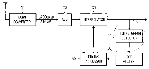
(0003] FIG. 1 illustrates a timing restoring device of a vestigial sideband
(VSB) type digital
receiver. A signal received through an antenna is converted to a baseband
signal through a
down converter 10. The down converted baseband signal is then converted to a
digital
signal by an A/D converter 20. The down converter 10 may be exchanged with the
A/D
converter 20 such that the received signal may be converted to the digital
signal first, and
then converted to the baseband signal.
[0004] The sample timing of the baseband signal is then corrected by an
interpolator 30,
and the baseband signal having the corrected sample timing is then input to
the timing error
detector 40. The timing error detector 40 then detects a timing error of the
signal input
thereto. The timing error detector 40 provides the signal to a loop filter 50,
and a timing
processor 60 calculates a proper sample timing using an output of the loop
filter 50. The
timing processor 60 provides the proper sample timing to the interpolator 30.
As a result, the
timing error generated in the A/D converter 20 of the digital receiver is
corrected.
[0005] In particular, in order to correct the timing error efficiently, it is
important that the
timing error detector 40 precisely detect the timing error.
[0006] FIG. 2 illustrates a conventional method of detecting the timing error,
and FIG. 3
illustrates another conventional method of detecting the timing error.
CA 02510496 2005-06-22
[0007] FIG. 2 illustrates the Gardner timing error detection algorithm.
According to the
Gardner timing error detection algorithm, a current signal has a sampling rate
that is two
times greater than a data rate of the baseband. The current signal is input,
and a signal that
is two samples before the current signal (i.e., delayed by a first delay unit
41 and a second
delay unit 43) is subtracted therefrom by a subtractor 45 to obtain a
difference signal. A data
rate of the signal that is two samples before the current signal is equal to a
data rate of a
signal that is one sample before the current signal. The difference signal is
then multiplied
by the signal that is one sample before the current signal (i.e. delayed by
the first delay unit
41 ) by a multiplier 47 to obtain an output signal. As a result, the output
signal indicates a
degree of timing error of the current signal.
[0008] The Gardner algorithm serves to restore timing of a signal having multi
levels, which
may be expressed as the following equation 1.
Equation 1
ay(r)=YI(r-1/2)~YI(y') YI(r-1)~+YQ(~"-1/2)~YQ(~") YQ(~"-1)~
(0009] In this case, the timing error is calculated based on a real number
part (I) and an
imaginary number part (Q), because a received VSB signal or an orthogonally
quadrature
amplitude modulation (OQAM) signal includes the real number part (I) and the
imaginary
number part (Q). The timing error is detected for each part and the timing
error for each
part is added together. When the timing error is detected as described above,
the timing
error may be detected in a quadrature phase shift keying (QPSK) or a QAM
signal almost
regardless of an effect that results from a phase error or a carrier frequency
error.
[0010] However, the Gardner timing error detection algorithm is severely
affected by a
broadcast wave frequency error and/or the phase error in a VSB system, the
OQAM system,
or the like. This may result from characteristics of the VSB signal or the
OQAM signal.
[0011] FIG. 4 is a diagram illustrating a characteristic of the VSB signal or
the OQAM signal.
Referring to FIG. 4, data in the VSB signal or the OQAM signal are alternately
carried in the
real number part (I) and the imaginary number part (Q). Black dots illustrated
in FIG. 4
indicate the carried data while blank dots indicate parts where the data is
not carried.
[0012] Referring to FIG. 4, the data is alternately carried in the real number
part (I) and the
imaginary number part (Q) of the VSB signal or the OQAM signal such that the
timing error
detection is affected by the carrier frequency error and the phase error when
the timing error
detection is performed on the signals using the Gardner algorithm. In the VSB
signal or the
OQAM signal one of the real number part (I) and the imaginary number part (Q)
carries data
2
CA 02510496 2005-06-22
while the other does not carry data such that the carrier frequency error and
the phase error
terms do not cancel each other out. Thus, the uncanceled carrier frequency
error and phase
error terms affect the timing error detection, thereby degrading performance
of the timing
restoring device in a channel environment in which the carrier frequency error
occurs and
the phase error occurs.
[0013] Unlike the VSB or the OQAM signals the data is carried in both of the
real number
part (I) and the imaginary number part (Q) in the QPSK signal or the QAM
signal (i.e.,
without alternating) such that the carrier frequency error terms are canceled
off.
[0014] FIG. 3 illustrates an early late timing error detection algorithm that
uses a known
signal between a receiver and a transmitter. The early late timing error
detection algorithm
may also be applied to a signal which is not known by preprocessing the
signal.
[0015] The early late timing error detection algorithm is a timing error
detection method that
uses a feature in which a signal value before a proper sampling time is equal
to a signal
value after the proper sampling time. According to the early late timing error
detection
algorithm, a signal having a sampling rate equal to or greater than the data
rate of the
baseband is input to extract a known signal, or is input through a proper
signal
preprocessing procedure to extract a signal that is suitable for the early
late algorithm to be
applied. A difference between the signal value right before and right after
the proper
sampling timing is calculated as the timing error signal.
[0016] The early late timing error detection algorithm may be varied in
response to the
signal preprocessing procedure. The Gardner timing detection algorithm is one
of these
variations.
[0017] The early late timing detection algorithm as well as the Gardner timing
detection
algorithm have poor characteristics with respect to the carrier frequency
error and the phase
error. This results from the fact that the timing error is extracted using a
signal waveform
when the early late timing error detection algorithm is used, and the timing
error may not be
precisely detected due to a distortion of the signal waveform when the carrier
frequency
error and the phase error are present in the signal to be extracted. As a
result, even when
the timing error is extracted based on the known signal, the timing error may
not be precisely
detected when the carrier frequency error or the phase error are present.
3
CA 02510496 2005-06-22
SUMMARY OF THE INVENTION
[0018] The present general inventive concept provides a symbol timing error
detector to
correct a symbol timing drift using a channel profile regardless of a carrier
frequency offset,
and a method of detecting a symbol timing error.
[0019] Additional aspects of the present general inventive concept will be set
forth in part in
the description which follows and, in part, will be obvious from the
description, or may be
learned by practice of the general inventive concept.
[0020] The foregoing and/or other aspects of the present general inventive
concept are
achieved by providing a symbol timing error detector, which includes a non-
coherent
correlator to calculate a non-coherent correlation value of a received signal
using a pseudo
noise (PN) sequence that is divided into a predetermined number of units to
calculate a
channel profile, a block buffer to window and store a predetermined portion of
the channel
profile, a profile comparison unit to compare the channel profile stored in
the block buffer
with a current channel profile output from the non-coherent correlator using
pattern
matching, and a symbol timing estimator to detect a symbol index difference
determined
using the pattern matching of the channel profile as a symbol timing drift.
[0021] The non-coherent correlation value calculated by the non-coherent
correlator may be
obtained according to:
N K
ri (~)Pi (k)
i=1 n=I
where r(k) is the received signal, p(k) is the PN sequence, N is the number of
symbols in the
PN sequence for each of the units, and K is the predetermined number of units.
[0022] In addition, the non-coherent correlator may calculate the non-coherent
correlation
value using a subsequence according to:
P(n) _ (PI (nl )~ Pz (nz )~..., Pn (nN )
1<_n_<M
15n; 5K(i=1,2,...,1
where p(n) is the PN sequence, K is the predetermined number of units, and N
is a number
of symbols in the subsequence.
[0023] The symbol timing error detector may further include a quantization
unit to quantize
the channel profile to reduce an amount of calculation performed by the
profile comparison
unit.
4
CA 02510496 2005-06-22
[0024] The foregoing and/or other aspects of the present general inventive
concept are also
achieved by providing a method of detecting a symbol timing error, which
includes
calculating a non-coherent correlation value of a received signal using a
pseudo noise (PN)
sequence that is divided into a predetermined number of units to calculate a
channel profile,
windowing and storing a predetermined portion of the channel profile,
comparing the stored
channel profile with a current channel profile, and detecting a symbol index
difference
determined using the pattern matching of the current channel profile and the
stored channel
profile as a symbol timing drift.
[0025] Accordingly, the channel profile is calculated using the non-coherent
correlation,
which is used to detect the symbol timing drift such that the timing error may
be corrected
regardless of a carrier frequency offset that results from an effect of a
channel environment.
BRIEF DESCRIPTION OF THE DRAWINGS
[0026] These and/or other aspects and advantages of the present general
inventive concept
will become apparent and more readily appreciated from the following
description of the
embodiments, taken in conjunction with the accompanying drawings of which:
[0027] FIG. 1 is a diagram illustrating a timing restoring device of a digital
receiver;
[0028] FIG. 2 and FIG. 3 illustrate conventional methods of detecting a timing
error;
[0029] FIG. 4 is a diagram illustrating characteristics of a VSB signal and a
OQAM signal;
[0030] FIG. 5 is a schematic block diagram illustrating a symbol timing error
detector
according to an embodiment of the present general inventive concept;
[0031] FIG. 6 and FIG. 7 are diagrams illustrating operations of the symbol
timing error
detector of FIG. 5 according to an embodiment of the present general inventive
concept; and
[0032] FIG. 8 is a flow chart illustrating a method of detecting a symbol
timing error
according to an embodiment of the present general inventive concept
DETAILED DESCRIPTION OF THE PREFERRED EMBODIMENTS
[0033] Reference will now be made in detail to the embodiments of the present
general
inventive concept, examples of which are illustrated in the accompanying
drawings, wherein
like reference numerals refer to the like elements throughout. The embodiments
are
described below in order to explain the present general inventive concept by
referring to the
figures.
CA 02510496 2005-06-22
[0034] FIG. 5 is a schematic block diagram illustrating a symbol timing error
detector
according to an embodiment of the present general inventive concept.
[0035] Referring to FIG. 5, the symbol timing error detector includes a non-
coherent
correlator 110, a quantization unit 120, a block buffer 130, a profile
comparison unit 140, and
a symbol timing estimation unit 150.
[0036] The non-coherent correlator 110 receives a symbol signal and performs a
non-
coherent correlation on a field sync signal of the received symbol signal to
calculate a
channel profile. The received symbol signal may be a VSB digital TV signal.
Other signals
(e.g., an OQAM signal) may also be received. The non-coherent correlator 110
performs a
non-coherent correlation process to obtain the channel profile regardless of a
carrier
frequency offset. The non-coherent correlator 110 uses a partial non-coherent
correlation.
This is described below in detail.
[0037] The quantization unit 120 applies a threshold value to the channel
profile calculated
by the non-coherent correlator 110 and/or performs a quantization process to
reduce an
amount of calculation required. Accordingly, the quantization unit 120 reduces
the amount
of calculation amount performed by the profile comparison unit 140 by
eliminating relatively
low level values of the calculated channel profile that correspond to noise
components from
among a plurality of levels. The quantization unit 120 can also process the
calculated
channel profile having the plurality of levels to include integer values
(instead of decimal
values), because the channel profile calculated by the non-coherent correlator
110 includes
decimal numbers.
[0038] The block buffer 130 allows a channel profile calculated from a
previous field to be
stored such that the previous channel profile can be compared with the channel
profile
calculated from a current field. In this case, an overall channel profile may
be stored:
Alternatively, a predetermined portion of the channel profile may be windowed
and stored.
In addition, a magnitude of the predetermined portion to be stored may be
varied according
to an appropriate timing error correction range.
[0039] The profile comparison unit 140 compares the previous channel profile
stored in the
block buffer 130 with the current channel profile calculated by the non-
coherent correlator
110 using pattern matching. A pattern matching range is set according to the
appropriate
timing error correction range.
[0040] The symbol timing estimation unit 150 detects an index difference
between the
current channel profile that is pattern matched by the profile comparison unit
140 with the
previous channel profile stored in the block buffer 130 to detect an amount of
symbol timing
6
CA 02510496 2005-06-22
drift. The symbol timing drift is generally represented as the timing error
with respect to a
plurality of symbols. Additionally, the symbol timing error detector according
to embodiments
of the present general inventive concept corresponds to a coarse symbol timing
estimator
that determines the symbol timing error.
[0041] FIG. 6 and FIG. 7 are diagrams illustrating operations of the symbol
timing error
detector of FIG. 5 according to an embodiment of the present general inventive
concept.
FIG. 8 is a flow chart illustrating a method of detecting the symbol timing
error according to
an embodiment of the present general inventive concept. In some embodiments of
the
present general inventive concept, the method of FIG. 8 can be performed by
the symbol
timing error detector of FIG. 5. Thus, the method of FIG. 8 is described below
with reference
to FIG. 5. Hereinafter, the symbol timing error detector according to the
present general
inventive concept will be described in detail with reference to the drawings.
[0042] When the received symbol signal (e.g., a VSB signal) is input to the
symbol timing
error detector (operation S210), the non-coherent correlator 110 calculates
the non-coherent
correlation value for a field to calculate the channel profile that
corresponds to the field
(operation S220).
[0043] A number M pseudo-noise (PN) signals among field sync signals are
divided into
symbols in order based on a K unit, which are represented as a subsequence
"p(n)"
including N symbols as expressed in the equation 2 below.
Equation 2
P(n) _ (P~ (ni )~ Pz (nz )~..., Pn (nN )
1<_n<_M
1<_n; <_K(i=1,2,...,N)
[0044] The subsequence "p(n)" is then used with respect to a received signal
"r(k)" to
calculate a partial coherent correlation value based on the equation 3 below.
Equation 3
N K
~'"a(k)Pr(k)~
r=~
[0045] Accordingly, a range of the carrier frequency offset capable of
calculating the channel
profile depends on a magnitude of K. However, almost the same offset range may
be
obtained regardless of whether the carrier frequency offset is within an
estimated range. In
this case, an absolute value is calculated with respect to the partial
coherent correlation
7
CA 02510496 2005-06-22
value. The absolute value includes a complex power of the partial coherent
correlation
value.
[0046] Next, a quantization process can be performed by the quantization unit
120 such that
a predetermined threshold value is applied to the calculated channel profile
to remove noise
components and to reduce an amount of calculation necessary for pattern
matching. The
predetermined threshold value or the quantization process that can be applied
may be
determined according to an amount of calculation necessary for timing error
detection,
hardware complexity, required accuracy, or the like. A predetermined portion
of the
processed channel profile where a main path is included can then be windowed
and stored
in the block buffer 130. The profile comparison unit 140 then performs pattern
matching
between the channel profile of the current field and the stored channel
profile of the previous
field (operation S230).
[0047] The predetermined portion of the channel profile that is stored for the
pattern
matching may correspond to a portion of the channel profile where the main
path is included,
and a window size may be varied according to the appropriate timing error
correction range.
FIG. 7 illustrates an operation of setting the window to be stored for the
pattern matching.
[0048] Referring to FIG. 6, based on the main path of the channel profile of
the current field
(i.e., an nt" field) and the channel profile of the previous channel (i.e., an
(n-1 )t" field) that are
matched using the pattern matching of operation S230, an index difference
between the
matched portions is detected as an amount of the timing drift that occurs for
one field of the
symbol signal as the timing error value (operation S240).
[0049] In addition, the amount of the timing drift detected may be accumulated
to calculate
an average value such that the timing error detection and correction may be
more accurately
performed.
[0050] The embodiments of the present general inventive concept use a non-
coherent
channel profile to detect and correct the timing drift regardless of the
carrier frequency offset
such that performance of a fine symbol timing recovery apparatus connected to
an output of
the symbol timing error detector may be improved. The symbol timing error
detector and the
method of detecting the symbol timing error according to various embodiments
of the
present general inventive concept may be included and/or used in a symbol
timing recovery
apparatus to recover symbol timing between a transmitting end and a receiving
end of a
digital broadcast system.
[0051] In general, if the timing offset compensation range is increased when
the symbol
timing is to be restored, a residual error typically increases. When the
residual error
8
CA 02510496 2005-06-22
increases, it takes several times to compensate for varying timing offset or
the timing offset
compensation range requires several times. However, according to the
embodiments of the
present general inventive concept, the timing drift is corrected such that the
timing offset
(about 1.92 ppm) may be decreased to within 0.5 symbols for each field even
when a
significantly large timing offset is present. In addition, when the timing
offsets with respect to
a plurality of fields are accumulated to obtain an average timing offset
value, the timing offset
may be decreased such that performance of the fine symbol timing recovery
circuit that is
connected to the receiving end may be improved.
[0052] The timing offset compensation range capable of being detected is
significantly
limited in a conventional symbol timing recovery apparatus, whereas the symbol
timing
recovery apparatus according to the present general inventive concept may
adjust a pattern
matching range of the channel profile such that detection and compensation of
a significantly
large timing offset may be implemented.
[0053] In addition, the symbol timing recovery in the conventional symbol
timing recovery
apparatus is typically affected by the carrier frequency offset, whereas the
symbol timing
recovery apparatus according to embodiments of the present general inventive
concept
operates regardless of the carrier frequency offset such that the symbol
timing error detector
may operate with a coarse carrier frequency offset recovery apparatus.
[0054] When a channel includes many multi paths, the performance of the symbol
timing
recovery apparatus can be degraded, however the symbol timing recovery
apparatus
according to embodiments of the present general inventive concept operates
regardless of a
complexity of the channel profile and is affected only by a change in an
amount of the non-
coherent channel profile for each field.
[0055] In addition, the symbol timing error detector may be applied to a
synchronization
detector to detect synchronization of a VSB signal using a non-coherent
correlation value
and/or may be applied to a symbol timing recovery algorithm or other carrier
frequency offset
recovery algorithm that uses a synchronization signal as a reference signal.
In addition,
selection and adjustment of the predetermined threshold value used to
eliminate noise
components in the non-coherent correlation value, the quantization process,
and the pattern
matching process may allow hardware complexity, an amount of calculation, and
an
accuracy to be adjusted.
[0056] According to the present general inventive concept, the channel profile
is calculated
using the non-coherent correlation, which is used to detect the symbol timing
drift, such that
9
CA 02510496 2005-06-22
the timing error may be corrected regardless of the can-ier frequency offset
that results from
an effect of the channel environment.
[0057) The embodiments of the present general inventive concept can be
embodied in
software, hardware, or a combination thereof. In particular, some embodiments
can be
computer programs and can be implemented in general-use digital computers that
execute
the programs using a computer readable recording medium. Examples of the
computer
readable recording medium include magnetic storage media (e.g., ROM, floppy
disks, hard
disks, etc.), optical recording media (e.g., CD-ROMs, DVDs, etc.), and storage
media such
as carrier waves (e.g., transmission through the Internet). The computer
readable recording
medium can also be distributed over network coupled computer systems so that
the
computer programs are stored and executed in a distributed fashion.
[0058) The foregoing embodiment and advantages are merely exemplary and are
not to be
construed as limiting the present general inventive concept. The present
teachings can be
readily applied to other types of apparatuses. Also, the description of the
embodiments of
the present general inventive concept is intended to be illustrative, and not
to limit the scope
of the claims, and many alternatives, modifications, and variations will be
apparent to those
skilled in the art. Although a few embodiments of the present general
inventive concept have
been shown and described, it will be appreciated by those skilled in the art
that changes
may be made in these embodiments without departing from the principles and
spirit of the
general inventive concept, the scope of which is defined in the appended
claims and their
equivalents.