Note: Descriptions are shown in the official language in which they were submitted.
CA 02511833 2005-06-08
SPECIFICATION
Components for a Film-forming Device and Method for Cleaning the Same
Technical Field of the Invention
The present invention relates to a component for a film forming equipment
which uses a film forming material to form various thin-films, and a method of
cleaning such a component.
Background Art
In a manufacturing process of semiconductor components used in large scale
integrated circuits (LSI), solar batteries, liquid crystal displays, plasma
displays and the
like, the film-forming equipments for forming thin films on substrates through
vapor
depositing, sputtering, CVD or other process with a film-forming materials has
been
used.
The aforementioned film-forming material has also formed a deposited film
over the surfaces of the components such as a buffer plates represented by a
substrate
mask and a wafer support frame in the film forming equipments when a thin film
has
been formed therein.
The aforementioned deposited film thickly accumulates on the components as
a number of substrates are successively processed to form films thereon in the
film
forming equipments. If the accumulated deposited film is broken at a certain
time point,
dust occurs. The dust may fall on a substrate on which a film is being formed,
resulting
in damage of the intended properties in the formed film. This reduces the
yield in the
manufacturing products.
To overcome such a problem, Japanese Laid-Open Patent Application No.
1991-87357 has proposed a structure in which a deposited film thickly
accumulated on
a component cannot easily be broken/separated from the surface of the
component as a
result of a mechanical process such as cutting or peeling or a blasting
process to the
surface of the component.
If the aforementioned processed component is used in the film forming
equipments, it is preferable in that the deposited film cannot easily be
broken/separated
from the surface of the component when a thin film is being formed.
Where the component from which the deposited film has been removed is to
be re-used, however, it is difficult to remove the deposited film through the
mechanical
removing process because the above structure is configured to prevent the
deposited
CA 02511833 2005-06-08
film being easily broken/separated in the first place.
A chemical removal process for dissolving an deposited film by use of a
cleaning fluid has also been proposed. Such a chemical process requires that a
component with a deposited film is dipped in the cleaning fluid for about two
days.
This is disadvantageous in that the component may be more dissolved than the
deposited film depending on the types of the cleaning fluid and deposited
film.
To overcome such a problem, Japanese Laid-Open Patent Application No.
1999-124661 has proposed a component in which, to remove the deposited film
while
suppressing the dissolution of the component itself, the surface of a matrix
metal
material (e.g., aluminum or its alloy) in the aforementioned component is
covered with
a lower readily-soluble metal layer consisted of a metal more easily soluble
in acid
cleaning fluid than the matrix metal material (e.g., copper or its alloy), a
porous metal
film being then formed over the lower readily-soluble metal layer (e.g., see
Patent
document 2).
When the cleaning fluid reaches the lower readily-soluble metal film layer
from the edges of the component and surface defects of a deposited film, it
dissolves
this lower readily-soluble metal film layer at the first time.
Therefore, the deposited film can be separated from the component for a
shorter time period. In the aforementioned component according to the prior
art,
however, time period required to separate the deposited film from the
component after
the cleaning fluid has reached the lower readily-soluble metal film layer via
the
aforementioned porous metal film to dissolve the lower readily-soluble metal
film
layer is between 5 and 15 hours. Thus, time period for which the component is
dipped
in the cleaning fluid can certainly be shortened. However, the component must
yet be
dipped in the cleaning fluid for a long time, resulting in not a little damage
to the
matrix metal material.
Furthermore, the damage to the matrix metal material also results from the
selection of material for the aforementioned lower readily-soluble metal film
layer.
In other words, the prior art selected a metal more easily soluble into the
acid
cleaning fluid than the matrix metal material as the material for the
aforementioned
lower readily-soluble metal film layer. If the matrix metal material is
aluminum or its
alloy and when the component is dipped in the cleaning fluid for a long time,
however,
a local cell will be formed between the matrix metal material of aluminum or
its alloy
and the lower readily-soluble metal film layer of copper or its alloy by the
potential
difference since the aluminum is less noble than the copper or its alloy as
can be seen
from the natural electrode potential. This may more dissolve the matrix metal
material.
2
CA 02511833 2005-06-08
An object of the present invention is thus to provide a component for a film
forming equipment having a structure which can separate a deposited film from
the
component for a time period shorter than that of the prior art and reduce the
damage to
the matrix metal material from the cleaning fluid, and a method of cleaning
such a
component.
Disclosure of the Invention
To overcome the aforementioned problems of the prior art, the component
according to the present invention which is to be used in a film forming
equipment for
forming a thin film is characterized by that it comprises the surface of a
matrix metal
material formed with a metal film layer electrochemically less noble than the
matrix
metal material through a spraying, vapor depositing, sputtering, laminating or
other
process.
In such an arrangement, if the processed component is dipped in a cleaning
fluid, a local cell is formed between the matrix metal material and the
aforementioned
metal film layer by a natural electrode potential difference therebetween,
with the local
current then flowing from the matrix metal material to the metal film layer.
On the other hand, the metal film layer preferentially dissolves and remains
in
the cleaning fluid as metal ions.
In general, when a local cell is formed between two different metals, one of
these metals less noble than the other and having its larger natural electrode
potential
difference will more rapidly be dissolved.
Therefore, the materials for the aforementioned metal film layer may suitably
be selected in consideration with the type of matrix metal material and the
potential
difference between the matrix metal material and the deposited film.
By forming a second metal film layer electrochemically more noble than the
aforementioned matrix metal material on the surface of the aforementioned
metal film
layer through a thermal spraying, vapor depositing, sputtering, laminating or
other
process, a local cell is also formed between the second metal film layer and
the lower
metal film layer. Thus, the dissolution advances from both the interfaces
between the
lower metal film layer and the matrix metal material and between the lower
metal film
layer and the second metal film layer.
At this time, the potential difference between the second metal film layer and
the lower metal film layer becomes larger than the potential difference
between the
matrix metal material and the lower metal film layer. Thus, the dissolution
will more
intensely advance in the vicinity of the interface between the second metal
film layer
3
CA 02511833 2005-06-08
and the lower metal film layer.
Now, if the potential in the deposited film is higher than that of the matrix
metal material (for example, if the deposited film is made of molybdenum and
the
matrix metal material is aluminum or its alloy) and if the potential of the
second metal
film layer is higher than that of the matrix metal material, the matrix metal
material
becomes less noble than those of the deposited film and second metal film
layer,
resulting in the potential of the matrix metal material being lower than that
of the
deposited film or second metal film layer. This may cause the matrix metal
material to
be dissolved by the cleaning fluid.
In such a case, thus, the dissolution may be avoided by applying a positive
electric field to the matrix metal material and immobilizing the matrix metal
material
so that it behaves as a metal more noble than the deposited film or second
metal film
layer.
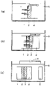
Brief Description of the Drawings
Figs. 1(a), (b) and (c) are cross-sectional views, partially enlarged, of a
component according to the present invention: Fig. 1(a) shows the component
when it
is dipped in a cleaning fluid after a metal film layer has been formed on the
surface of
a matrix metal material; Fig. 1(b) shows the component when it is dipped in
the
cleaning fluid after the second metal film layer has been formed on the
surface of the
metal film layer; and Fig. 1(c) shows a cleaning process for removing the
deposited
film by applying a positive electric field to the matrix metal material.
Best Mode for Carrying Out the Invention
Fig. 1(a) is an enlarged cross-sectional view of a component for a film
forming equipment in which a metal film layer 2 is formed on the surface of a
matrix
metal material 1. The component comprising the matrix metal material 1 may
include
buffer plates such as substrate masks in the film forming equipment or wafer
support
frame. When a thin film is formed on a substrate from a film forming material
in the
film forming equipment, a deposited film d also~deposits on the aforementioned
component in addition to the substrate.
This deposited film thickly accumulates on the component as a number of
substrates are successively processed to form films thereon in the film
forming
equipment. If the accumulated deposited film is broken at a certain time
point, dust
occurs. The dusts may fall on the substrate being processed to damage the
intended
properties of the formed film.
4
CA 02511833 2005-06-08
To remove this adhesion film d, the matrix metal material 1 may be dipped in
a cleaning fluid S. However, the matrix metal material 1 must be dipped in the
cleaning
fluid S for a considerable time period (e.g., about two days) until the
cleaning fluid S
sufficiently penetrates into the deposited film d to separate it from the
matrix metal
material 1. This may also damage the matrix metal material.
Furthermore, the time period for which the matrix metal material 1 must be
dipped in the cleaning fluid S may be shortened by forming a lower readily-
soluble
metal film layer on the surface of the matrix metal material 1 and further
forming a
porous metals film on the surface of this lower readily-soluble metal film
layer. Even
in such a case, time required to separate the deposited film from the matrix
metal
material 1 is in a range between 5 hours and 15 hours. This means that the
component
must be yet dipped in the cleaning fluid S for a long time, resulting in not a
little
damage to the matrix metal material 1.
A preferred material for forming the aforementioned lower readily-soluble
metal film layer is a metal more readily soluble to the cleaning fluid S than
the matrix
metal material 1, for example, a copper alloy. If the matrix metal material 1
is or an
aluminum alloy, the natural potential electrode measurement data show that
copper
alloy (JIS A5052 is -1.02 in one mol/1 of sulfuric acid liquid) is more noble
than or an
alloy of aluminum (JIS A5052 is -1.70 in one mol/1 of sulfuric acid liquid),
as shown
in Table 1. If the matrix metal material 1 of or an alloy of aluminum is
dipped in the
cleaning fluid for a long time, therefore, a local cell may be formed between
or an
alloy of aluminum and or an alloy of copper from the potential difference
therebetween
to promote the oxidization so that the matrix metal material 1 will more be
dissolved.
It is intended herein that a more noble metal is one located above the
reference
metal in the table 1 while a less noble metal is one located below the
reference metal in
the table 1. Thus, whether a metal is more or less noble is determined
relative to the
reference metal.
The present invention can separate the deposited film d from the matrix metal
material 1 along with the metal film layer 2 for a shortened time period
(e.g., about 45
minutes) by forming a metal film layer 2 containing a metal less noble than
the matrix
metal material 1 on the surface of the matrix metal material 1 through thermal
spraying,
vapor depositing, sputtering, laminate or other process and by causing a local
cell to be
formed between the matrix metal material 1 and the metal film layer 2 to
promote the
dissolution of the metal film layer 2 when the matrix metal material 1 is
dipped in the
cleaning fluid S.
In other words, the local cell is formed between the matrix metal material 1
CA 02511833 2005-06-08
and metal film layer 2 by the potential difference therebetween, the local
current then
flowing from the matrix metal material 1 to the metal film layer 2.
On the other hand, the metal film layer preferentially dissolves and remains
in
the cleaning fluid as metal ions.
For example, if the metal film layer 2 is Al -5% In (its natural potential is
-1.17 in one mol/I of sulfuric acid liquid) and the matrix metal material 1 is
A1 alloy
(the natural electrode potential of JIS A5052 is -0.70 in one mol/1 of
sulfuric acid
liquid) and when the deposited film d of 99.99%Al (4N-Al) (its natural
potential is -
0.86 in one mol/1 of sulfuric acid liquid) deposits over the metal film layer
2, a local
cell is formed between the matrix metal material 1 and the metal film layer 2
in the
sulfuric acid liquid. The metal film layer 2 is ionized and dissolved into the
sulfuric
acid liquid.
The metal film layer 2 may suitably be selected from a group consisting of
metals and alloys that can easily form the local cell between the metal film
layer 2 and
the matrix metal material 1, based on the natural potential E (Vvs.SCE) in the
cleaning
fluid S.
Referring now to Fig. 1(b), there is shown a second metal film layer 3 formed
on the surface of the aforementioned metal film layer 2 through thermal
spraying,
vapor depositing, sputtering, laminating or other process, the second metal
film layer 3
containing a metal more noble than the matrix metal material 1.
In this case, since, in the cleaning fluid S, a local cell is formed between
the
metal film layer 2 and the matrix metal material 1 and another local cell is
also formed
between the metal film layer 2 and the second metal film layer 3, the
dissolution
advances from both the interfaces between the metal film layer 2 and the
matrix metal
material 1 and between the metal film layer 2 and the second metal film layer
3, the
deposited film d can be separated from the matrix metal material 1 more
rapidly than
the case of Fig. 1(a) that only the metal film layer 2 is formed.
For example, if the metal film layer 2 is Al-5%In; the second metal film layer
3 is A1 alloy (the natural potential of JIS A2017 is -0.56 in one mol/1 of
sulfuric acid
liquid); and the matrix metal material 1 is A1 alloy (JIS A5052) and when
99.99%Al
(4N-Al) film deposits on the second metal film layer 3, local cells are formed
between
the matrix metal material 1 and the metal film layer 2 and between the second
metal
film layer 3 and the metal film layer 2, respectively, in the sulfuric acid
liquid. Thus,
the metal film layer 2 is ionized and dissolved into the sulfuric acid liquid.
At this time, time required to dissolve the metal film layer 2 and separate
the
deposited film d from the matrix metal material 1 was about 15 minutes.
6
CA 02511833 2005-06-08
Referring now to Fig. 1(c), reference numeral 4 denotes a power source for
applying a positive electric field to the matrix metal material 1 so that it
will function
as anode. The negative side of the power source 4 is connected to a cathode 5.
If the deposited film d has its potential higher than that of the matrix metal
material 1 or if the second metal film layer 3 has its potential higher than
that of the
matrix metal material 1, the matrix metal material 1 may be less noble than
the
deposited film d or the second metal film layer 3. In this case, the matrix
metal
material 1 may dissolve into the cleaning fluid S.
However, this can be avoided by applying a positive electric field from the
power source 4 to the matrix metal material 1 so that the matrix metal
material 1 will
be immobilized to behave as a metal more noble than the deposited film d or
the
second metal film layer 3.
As will be apparent from the above description, the present invention can
separate the deposited film d from the matrix metal material 1 for an
extremely
shortened time period, without damaging the matrix metal material 1 itself
from the
cleaning fluid S by providing the aforementioned metal film layer 2 on the
surface of
the matrix metal material 1 of the component to form the local cell between
the metal
film layer 2 and the matrix metal material 1 or by providing the second metal
film
layer 3 on the surface of metal film layer 2 to form the local cell between
the metal
film layer 2 and the second metal film layer 3. Thus, it can be promoted to
reuse the
component while the life thereof can be extended.
Industrial Applicability
As described, the present invention provides the component for the filin
forming equipments and the method of cleaning the same are suitable for use in
formation of the thin film on the substrate such as buffer plate (e.g.,
substrate mask) or
wafer support plate from the film forming material through vapor depositing,
sputtering, CVD or other process since the deposited film can be separated
from the
film forming equipment component for a shortened time period so that the
matrix
metal material can be less damaged by the cleaning fluid and since the
components of
the present invention and method thereof are led to extend the life of the
components,
reduce the running cost for the film forming equipment, and save the resource.
7
CA 02511833 2005-06-08
Table 1
In one mol/I of In two mol/I of
sulfuric acid liquid , nitric acid liquid
(-0.02)Cu
(-0.06)Cu-7%AI
Ni
-0.13)Ni
A2017(-0.2
(-0.56)A2017
A5052(-O.fi5
-0.68)LMA5.
-0.70)A5052
-0.86)4NAI ~--- AI-5%In(-0.84)
(-1.17)AI-5%In
-1.26 AI-1 %In
(-1.30)AI-0.5%In
Natural Electrode potential : E (Vvs. SCE)
s