Note: Descriptions are shown in the official language in which they were submitted.
CA 02511944 2005-06-27
DESCRIPTION
TITLE OF THE INVENTION
WAVE TRANSMISSION MEDIUM AND WAVEGUIDE CIRCUIT
TECHNICAL FIELD
The present invention relates to a wave transmission
medium and a waveguide circuit using it, and a
fabrication method thereof, and more particularly to
a medium for transmitting waves using multiple
scattering in accordance with two-dimensional
refractive index distribution and a waveguide circuit
configured using it, and to a f abrication method thereof .
BACKGROUND ART
In a technical field such as optical communication,
integrated optical components utilizing an optical
waveguide structure have been developed to construct
optical circuits for easily implementing optical
splitting and interference. The integrated optical
components utilizing the property of waves make it to
adjust optical path length and to facilitate fabrication
of interferometers. In addition, applying the
semiconductor circuit processing technique enables
integration of optical components.
However, since these optical waveguide circuits
construct individual components of optical circuits
using an "optical confinement structure" that carries
1
CA 02511944 2005-06-27
out the spatial optical confinement of light propagating
through an optical waveguide by utilizing the spatial
distribution of refractive index, a cascaded circuit
design using optical wiring is required. Consequently,
it is inevitable that optical path length of the optical
waveguide circuit becomes longer than the optical path
length required for bringing about interference in the
optical circuit. This presents a problem of sharply
increasing the size of the optical circuit.
io For example, take a typical arrayed waveguide
grating as an example. The light including a plurality
of wavelengths (A ) input to an input port repeats
demultiplexing/multiplexing through star couplers
using slab waveguides, and demultiplexed optical waves
are output from an output port. In this case, an optical
path length required to demultiplex the optical waves
at a resolution of an order of one thousandth of the
wavelength becomes several tens of thousands of the
wavelength of the light propagating through the
waveguide. Furthermore, it is necessary not only to
carry out waveguide patterning of the optical circuit,
but also to perform such processing as providing a wave
plate for correcting the circuit characteristics that
depend on the polarization state (see, for example, Y.
Hibino, "Passive optical devices for photonic networks",
IEIC Trans. Commun., Vol. E83-B No. 10, (2000)).
In addition, since it is necessary to closely
2
CA 02511944 2005-06-27
confine the light within the waveguide to miniaturize
the optical circuit, the optical waveguide must have
a very large refractive index difference to control the
optical confinement state by the spatial distribution
of the refractive index. For example, a conventional
step-index optical waveguide is designed such that it
has the spatial distribution of the refractive index
that will make the refractive index difference greater
than 0.1%. The optical confinement utilizing such a
large refractive index difference presents a problem
of reducing the flexibility of a circuit configuration.
In particular, when implementing the refractive index
difference in optical waveguide by local ultraviolet
irradiation, thermooptic effector electrooptic effect,
the amount of change in the resultant refractive index
is about 0.1% at best. Accordingly, to change the
propagation direction of light, it must be gradually
varied along the optical waveguide. Thus, the optical
circuit inevitably becomes long, which makes it
difficult to miniaturize the optical circuit.
Furthermore, an optical circuit including a
grating-like circuit in addition to an optical waveguide
circuit is built on a basis of a periodic structure that
is substantially parallel to the propagation direction
of light, or of the periodic variation in a dielectric
refractive index. In addition, in an actual design,
the characteristics of the optical circuit are usually
3
CA 02511944 2005-06-27
achieved by a strictly periodic structure evaluable by
Fourier transform, or by a chirped structure that
distorts the periodicity slightly. Consequently, the
optical circuit has a substantially uniform structure
for a wave front, thereby making it difficult to control
the light in the direction perpendicular to the
propagation direction (in the direction of the
wavefront). For example, an optical circuit disclosed
in T. W. Mossberg, "Planar holographic optical
io processing", Optics Letters, Vol. 26, No. 7, pp. 414-416
(2001) cannot utilize the light that propagates through
the optical circuit without reflection as signal light
because it spreads in the circuit. In addition, as for
a circuit that varies a spot position sharply in a
direction perpendicular to the propagation direction,
such as a branching circuit, since the optical field
must be greatly expanded in the direction perpendicular
to the propagation direction, the size of the circuit
inevitably becomes large. Furthermore, in the actual
circuit design, only a design method is applicable which
is nearly equivalent to the design method of a
conventional linear grating circuit such as a fiber
grating. Thus, the design is limited to a circuit with
a strictly periodic structure (that is, an optical
circuit depending on the wave number in the propagation
direction). This increases the circuit scale, makes
the circuit sensitive to the wavelength, and has the
4
CA 02511944 2005-06-27
input/output positions distributed sequentially in
accordance with the wavelengths, thereby presenting a
problem of limiting the design to circuits with little
flexibility.
On the other hand, optical wavelength division
multiplexing communication systems using a plurality
of optical wavelengths have been developed actively to
increase communication capacity. Such an optical
wavelength division multiplexing communication system
employs an arrayed waveguide grating type optical
multi/demultiplexing circuit as an optical wavelength
multi/demultiplexing circuit for multiplexing optical
signals with a plurality of wavelengths at a transmitter
side, and for demultiplexing the plurality of optical
signals propagating through an optical fiber to
different ports at a receiver side.
Fig. 1 is a diagram illustrating a configuration
of a conventional arrayed waveguide grating type optical
multi/demultiplexing circuit (see, for example, K.
Okamoto, "Fundamentals of Optical Waveguides",
Academic Press (2000)). The circuit comprises on a
substrate 100 an input waveguide 101, a first slab
waveguide 102, arrayed waveguides 103, a second slab
waveguide 104 and output waveguides 105, which are
connected in this order.
The light launched into the input waveguide 101
is expanded by the first slab waveguide 102, and is
5
CA 02511944 2005-06-27
demultiplexed to the arrayed waveguides 103 composed
of waveguides configured based on individual
wavelengths. Then, the outputs of the arrayed
waveguides 103 are multiplexed by the second slab
waveguide 104 again to be led to the output waveguides
105. Here, the optical field pattern projected to the
end of the first slab waveguide 102 on the side of the
arrayed waveguides 10 3 is basically reproduced (copied)
at the end of the second slab waveguide 104 on the side
of the arrayed waveguides 103. However, since the
arrayed waveguides 103 are designed such that the optical
path lengths of their adjacent optical waveguides differ
by AL, the optical field has an inclination depending
on the wavelength of the input light. The inclination
causes the positions of the focuses the optical field
forms on the end of the second slab waveguide 104 on
the side of the output waveguides 105 to be changed for
the respective wavelengths, thereby enabling the
wavelength demultiplexing.
Such an arrayed waveguide grating type optical
multi/demultiplexing circuit has become an
indispensable optical component for an optical
multiplexing communication system that transmits an
optical signal with a plurality of wavelengths through
a single optical fiber. In addition, a variety of
extended-passband arrayed waveguide grating type
optical multi/demultiplexing circuits have been
6
CA 02511944 2005-06-27
proposed which increase the transmission wavelength
bandwidth of the arrayed waveguide grating type optical
multi/demultiplexing circuit as shown in Fig. 1.
Figs. 2A and 2B are diagrams illustrating a
configuration of a conventionally proposed
extended-passband arrayed waveguide grating type
optical multi/demultiplexing circuit (see, for example,
K. Okamoto and A. Sugita, "Flat spectral response
arrayed-waveguide grating multiplexer with parabolic
to waveguide horns", Electronics Letters, Vol. 32, No. 18,
pp. 1661-1662 (1996)).
As shown in Fig. 2A, the circuit is configured by
adding to the circuit as shown in Fig. 1 a parabolic
waveguide 106 as illustrated in Fig. 2B, which is placed
between the input waveguide 101 and the first slab
waveguide 102. In Fig. 2B, z denotes the propagation
direction of light.
Figs. 3A and 3B are diagrams illustrating optical
field distribution at an interface between the parabolic
waveguide 106 and slab waveguide 102a in the
configuration of Fig. 2A, in which z denotes the
propagation direction of light, and x denotes the
direction of a cross section of the waveguide
perpendicular to the z direction. As shown in Fig. 3B,
the optical field distribution has a double-peak profile .
The double-peak optical field is regenerated at the
output waveguide side of the second slab waveguide 104,
7
CA 02511944 2005-06-27
and is coupled to the output waveguides 105, thereby
implementing the extended transmission wavelength
band.
The extended-passband arrayed waveguide grating
type optical multi/demultiplexing circuit with the
above-mentioned conventional configuration, however,
has a large chromatic dispersion value due to the phase
distribution in the parabolic waveguide as illustrated
in Fig. 4. Since the chromatic dispersion provides
1o different delay times to signal spectral components,
the conventional extended-passband arrayed waveguide
grating type optical multi/demultiplexing circuit with
the large chromatic dispersion has a problem of bringing
about considerable optical pulse degradation.
DISCLOSURE OF THE INVENTION
The present invention is implemented to solve the
foregoing problems. An object of the present invention
is to provide an optical (wave) transmission medium for
implementing an optical circuit that is smaller in size
than an optical circuit using the conventional optical
waveguide circuit or plane holographic circuit, that
can arrange the input/output of light as flexibly as
possible, and that enables sufficiently highly
efficient optical signal control even with mild
refractive index distribution (with small undulations),
thereby implementing a highly efficient, compact
8
CA 02511944 2005-06-27
waveguide circuit, and providing an arrayed waveguide
grating type optical multi/demultiplexing circuit with
small chromatic dispersion.
To accomplish the foregoing object, according to
a first aspect of the present invention, there is
provided a wave transmission medium for outputting
incident light that is launched into an input side port
(input port) to a desired output side port (output port) ,
said port being defined as a location of a circuit at
1o which a cross section having desired optical
input/output is given, the wave transmission medium
comprising: a spatial refractive index distribution
determined such that the incident light launched into
the input port propagates through the wave transmission
medium with scattered multiple times, wherein local
positions in the wave transmission medium are designated
by virtual pixels defined by a virtual mesh; and the
spatial refractive index distribution of the wave
transmission medium is formed by refractive indices of
the individual pixels.
The refractive index distribution of the wave
transmission medium can be set such that a phase of a
forward propagating field of the incident light launched
into the input port matches a phase of a reverse
propagating field of emitted light phase conjugation
of at individual points of the wave transmission medium.
The refractive indices the pixels can take can be
9
CA 02511944 2005-06-27
one of a low refractive index (nL) or a high refractive
index (nH) , and the refractive index distribution can
be given by spatially placing pixels with the low
refractive index (nL) and pixels with the high refractive
index (nH) .
The pixels with the low refractive index (nL) can
have an existing probability of equal to or less than
30% in a propagation direction of the incident light
in the wave transmission medium.
The pixels can take a finite number of refractive
indices between a lower limit refractive index and an
upper limit refractive index, and the refractive index
distribution can be given by spatially placing pixels
with the refractive indices selected from among the
finite number of refractive indices.
The refractive index distribution can be determined
such that the incident light launched into the input
port is split to different output port locations at a
desired ratio.
The incident light launched into the input port
can be wavelength division multiplexed light composed
of a plurality of wavelengths, and the refractive index
distribution can be determined such that the optical
waves are demultiplexed to different output port
locations depending on the individual wavelengths of
the wavelength division multiplexed light.
The incident light launched into the input port
CA 02511944 2005-06-27
can be wavelength division multiplexed light composed
of a plurality of wavelengths, and the refractive index
distribution can be determined such that the wavelength
division multiplexed light are demultiplexed and split
to different output port locations at a desired ratio.
The incident light launched into the input port
can be polarization multiplexed light with a TE mode
and TM mode, and the refractive index distribution can
be determined such that the polarization multiplexed
light is demultiplexed to different output port
locations depending on individual polarized waves of
the polarization multiplexed light.
The incident light launched into the input port
can be polarization multiplexed light with a TE mode
and TM mode, and the refractive index distribution can
be determined such that individual polarized waves of
the polarization multiplexed light are demultiplexed
and split to different output port locations at a desired
ratio.
The wave transmission medium can be composed of
a dielectric.
According to a second aspect of the present
invention, there is provided a fabrication method of
the wave transmission medium in accordance with the
present invention, the fabrication method comprising:
a first step of obtaining, in the wave transmission
medium with an assumed initial refractive index
11
CA 02511944 2005-06-27
distribution, a field distribution 1 of the incident
light and a field distribution 2 resulting from the
emitted light virtually transmitted from the output port
in a reverse direction; a second step of determining
the refractive index distribution such that a phase
difference between the field distribution 1 and the field
distribution 2 is reduced at the individual points of
the wave transmission medium; and a third step of
carrying out, at the output port locations, successive
approximation of the refractive index distribution by
repeating the first step and the second step until an
error between the field distribution 1 and the field
distribution of the emitted light becomes less than a
desired value.
The second step can determine the refractive index
distribution by a steepest descent method using
individual refractive indices of the pixels as
variables.
According to a third aspect of the present invention,
there is provided a fabrication method of the wave
transmission medium in accordance with the present
invention, the fabrication method comprising: a first
routine and a second routine for carrying out successive
approximation of the refractive index distribution, the
first routine including: a first step of obtaining, in
the wave transmission medium with an assumed initial
refractive index distribution, a field distribution 1
12
CA 02511944 2005-06-27
of the incident light and a field distribution 2
resulting from the emitted light virtually transmitted
from the output port in a reverse direction; a second
step of revising the refractive index distribution such
that the phase of the field distribution 2 matches the
phase of the field distribution 1 at the locations in
the wave transmission medium; a third step of reobtaining
the field distribution 2 at the locations using the
revised refractive index distribution; a fourth step
of redefining the locations as new locations by shifting
the locations by a predetermined distance in the reverse
propagation direction; and a fifth step of carrying out
successive approximation of the refractive index
distribution by repeating first to fourth steps, and
the second routine including: a sixth step of obtaining,
in the wave transmission medium with the assumed
refractive index distribution determined in the first
routine, a field distribution 1 of the emitted light
(incident light) and a field distribution 2 resulting
from the emitted light virtually transmitted from the
output port in a reverse direction; a seventh step of
revising the refractive index distribution such that
the phase of the field distribution 1 matches the phase
of the field distribution 2 at the locations in the wave
transmission medium; an eighth step of reobtaining the
field distribution 1 at the locations using the revised
refractive index distribution; a ninth step of
13
CA 02511944 2005-06-27
redefining the locations as new locations by shifting
the locations by a predetermined distance in the forward
propagation direction; and a tenth step of carrying out
successive approximation of the refractive index
distribution by repeating sixth to ninth steps.
The second step can use: as the field distribution
2, a field distribution obtained by forwardly
transmitting through the refractive index distribution
before the successive approximation a field
distribution resulting from transmitting the emitted
light to an incidence plane through the refractive index
distribution before the successive approximation; and
as the field distribution 1, a field distribution
obtained by reversely transmitting through the
refractive index distribution before the successive
approximation a field distribution resulting from
transmitting the incident light to an emitting plane
through the refractive index distribution before the
successive approximation.
The fabrication method can further comprise a third
routine of repeating the first routine and the second
routine sequentially until an error between the field
distribution 1 and the emitted light field distribution
at the output port locations becomes less than a desired
value.
The field distribution 1 and the field distribution
2 can each incorporate reflected light components of
14
CA 02511944 2005-06-27
the incident light and reverse propagation light through
the wave transmission medium.
The initial refractive index distribution can be
assumed to be a random distribution.
The incident light launched into the input port
can be wavelength division multiplexed light consisting
of optical waves with a plurality of wavelengths, or
polarization multiplexed light consisting of polarized
waves with a TE mode and a TM mode; the successive
approximation of the refractive index distribution can
be carried out sequentially using the field distribution
2 that is defined for each of the optical waves with
the individual wavelengths or for each of the individual
polarized waves of the multiplexed light; and the
refractive index distribution can be determined such
that the optical waves constituting the multiplexed
light are demultiplexed to different output port
locations at a desired ratio.
According to a fourth aspect of the present
invention, there is provided a waveguide circuit that
is configured by two- dimensional placement of the wave
transmission medium in accordance with the present
invention on a substrate.
A multimode interference circuit can be configured
using the waveguide circuit.
According to a fifth aspect of the present invention,
the following optical circuits are configured using the
CA 02511944 2005-06-27
waveguide circuit in accordance with the present
invention.
That is, an optical bending circuit configured using
the waveguide circuit in accordance with the present
invention; an optical circuit, the refractive index
distribution of which is implemented by local refractive
index variations of the waveguide circuit based on
electrooptic effect; and an optical circuit, the
individual refractive indices of the pixels of which
are determined such that the light is confined in a
direction perpendicular to the substrate.
The virtual mesh can be composed of configuration
elements of a unit cell that form the waveguide region
in periodic repetition.
The unit lattice can have a quasi-periodic
structure.
The pixels can take one of two refractive index
values of a high refractive index (nH) and a low
refractive index (nL).
The pixels with the high refractive index can have
a size equal to or less than a wavelength of the light
propagating through the waveguide region.
A value given by the following expression can be
equal to or less than 0.1,
4
ma
where A is the wavelength of the propagation light, n
16
CA 02511944 2005-06-27
is the refractive index (nH) of the pixels with the high
refractive index, a is the height of the pixels with
the high refractive index, and q is a coefficient given
by q = (z/a) where z is an average distance of radiation
components of the field distribution of the propagation
light.
The pixels with the high refractive index can have
a shape of a polygon with n sides, where n is an integer
equal to or greater than three, wherein the pixels can
io be placed such that the sides each have an inclination
with respect to the propagation direction of the light
propagating through the waveguide region.
The shape of a polygon can be a square, and an angle
of the inclination can be 45 degrees.
The pixels can each have a desired size equal to
or greater than the region defined by the virtual mesh,
and some of the pixels can be placed at locations deviated
from lattice locations defined by the virtual mesh.
The pixels with the high refractive index (nH) can
comprise a waveguiding section including a first high
refractive index layer and a second high refractive index
layer which are stacked sequentially, the second high
refractive index layer having a refractive index lower
than the first high refractive index layer; and the
pixels with the low refractive index (nL) can comprise
a waveguiding section composed of the second high
refractive index layer, wherein a center of a diameter
17
CA 02511944 2005-06-27
of the optical field propagating through the waveguiding
section of the pixels with the high refractive index
(nH) and a center of a diameter of the optical field
propagating through the waveguiding section of the
pixels with the low refractive index (nL) can be both
placed on a same plane parallel to a surface of the
substrate.
The waveguide region can be composed of a dielectric
material that has an optical loss function or optical
io amplification function.
The dielectric material can have a complex
refractive index depending on the wavelength of light.
The waveguide region can have a structure comprising
a first low refractive index layer, a high refractive
index layer constituting the waveguide section and a
second low refractive index layer, which are stacked
sequentially, wherein the light can be confined in the
high refractive index layer by the first and second low
refractive index layers.
The high refractive index layer can have, on its
one of surface, relief-like patterning formed by
creating concave portions, wherein the spatial
refractive index distribution can be implemented by
employing the concave portions as the low refractive
index section, and regions other than the concave
portions as the high refractive index section.
The relief-like patterning can be formed on both
18
CA 02511944 2005-06-27
surface of the high refractive index layer.
The relief-like patterns formed on both sides of
the high refractive index layer can have patterns
different from each other.
The concave portions of the relief-like patterns
formed on both sides of the high refractive index layer
can have a same depth.
The pixels can be each divided into a plurality
of virtual sub-pixels having one of the high refractive
1o index (nH) and the low refractive index (nL), and the
refractive index distribution of the pixels can be
implemented by arrangement of the sub-pixels with the
two refractive indices.
In the pixels, a refractive index difference can
be varied over a distance equal to or greater than one
wavelength as a rate of change of the refractive index
difference, as a rate of spatial change of a propagation
constant in the proceeding direction of a wavefront of
the propagation light.
The pixels or the sub-pixels can each have a circular
cross section in a direction parallel to the substrate.
The pixels or the sub-pixels can each have a cross
section with a shape of smoothly varying curve in a
direction perpendicular to the substrate.
At least one of the first and second low refractive
index layers can be formed by stacking a plurality of
layers with different refractive indices.
19
CA 02511944 2005-06-27
The optical circuit can consist of an optical
circuit with a mutual broadcast delivery/broadcast
reception configuration having at least three
input/output ports, wherein the spatial refractive
index distribution can be established such that phases
of signals output from the input/output ports are
perpendicular to each other.
The optical circuit can consist of an optical
circuit with a mutual broadcast delivery/broadcast
reception configuration having at least three
input/output ports, wherein the spatial refractive
index distribution can be established such that when
phases of signals output from the input/output ports
are not perpendicular to each other, overlaps of the
output signals become minimum.
A branching ratio of the optical circuit can be
asymmetric.
The foregoing optical circuits can comprise an
amplification function.
The optical circuit can include a plurality of input
ports, and be configured such that input optical signals
launched into the plurality of input ports are output
from a same emitting plane, wherein the spatial
refractive index distribution can be established such
that the individual optical signals output from the
plurality of input ports have their phases adjusted to
be aligned with each other, in order to shape a profile
CA 02511944 2005-06-27
of the output optical field.
There is provided an optical circuit having the
optical circuit as defined the above placed at an input
side slab of an arrayed waveguide grating circuit,
wherein mutual phase differences between the plurality
of input ports are given by circuit lengths of the optical
waveguides of said optical circuit; and a repetition
period (free spectrum range) of the phase differences
given by the circuit lengths of said optical waveguides
1o agrees with a wavelength spacing of outputs of said
arrayed waveguide grating circuit, and centers of fields
of the outputs of said optical circuit vary periodically
to cancel out chromatic dispersion characteristics of
said arrayed waveguide grating circuit periodically at
the wavelength spacing of the outputs.
The spatial refractive index distribution can be
established such that it implements a field profile and
phase distribution that enable spot size conversion of
the output light.
According to a sixth aspect of the present invention,
there is provided an arrayed waveguide grating type
optical multi/demultiplexing circuit configured using
the waveguide circuit in accordance with the present
invention, the arrayed waveguide grating type optical
multi/demultiplexer comprising: an input waveguide, a
first slab waveguide, arrayed waveguides, a second slab
waveguide and output waveguides, which are connected
21
CA 02511944 2005-06-27
sequentially on a planar substrate; and a plurality of
scattering points with a refractive index higher than
a refractive index of the input waveguide, the scattering
points being placed in a connecting region between the
input waveguide and the first slab waveguide.
The scattering points can be disposed such that
an optical field distribution formed at an output end
of the input waveguide has an iso-phase wave front without
distortion, and an amplitude with double peaks.
The scattering points can have in the input
waveguide a two-dimensional configuration that has
nearly line symmetry with respect to a line extending
to the propagation direction of light.
The scattering points can each have a side equal
to or greater than 0.2 pm.
The planar substrate can consist of a silicon
substrate, and the optical waveguides can consist of
silica-based glass optical waveguides.
According to the present invention, the optical
(wave) transmission medium is provided that is smaller
in size than the conventional optical circuit using the
optical waveguide circuit or plane holographic circuit;
that can set up the optical input/output as flexibly
as possible; and that implements a waveguide circuit
enabling highly efficient optical signal control even
with a mild refractive index distribution (small
undulations of the refractive index difference). Thus,
22
CA 02511944 2005-06-27
it can implement a highly efficient, compact optical
circuit.
In addition, the arrayed waveguide type optical
multi/demultiplexer in accordance with the present
invention has a plurality of scattering points placed
in the input waveguide in accordance with the spatial
refractive index distribution. Thus, it controls the
phase and intensity of the propagation light
simultaneously, thereby being able to provide a low
1o dispersion arrayed waveguide type optical
multi/demultiplexer that can reduce the chromatic
dispersion.
BRIEF DESCRIPTION OF THE DRAWINGS
Fig. 1 is a diagram illustrating a configuration
of a conventional arrayed waveguide grating type optical
multi/demultiplexing circuit;
Figs. 2A and 2B are diagrams illustrating a
configuration of a conventionally proposed
extended-passband arrayed waveguide grating type
optical multi/demultiplexing circuit;
Figs. 3A and 3B are diagrams illustrating optical
field distribution at the interface between the
parabolic waveguide and slab waveguide in the circuit
configuration of Fig. 2A;
Fig. 4 is a graph illustrating chromatic dispersion
values of the conventional extended-passband arrayed
23
CA 02511944 2005-06-27
waveguide grating type optical multi/demultiplexing
circuit;
Figs. 5A-5C are diagrams illustrating a basic
concept and basic structure underlying a wave
transmission medium in accordance with the present
invention;
Fig. 6 is a diagram illustrating a configuration
of a conventional arrayed waveguide grating circuit;
Fig. 7 is a flowchart illustrating a calculation
io procedure for determining a spatial refractive index
distribution in the wave transmission medium in
accordance with the present invention;
Fig. 8 is a diagram illustrating an example of a
field in the wave transmission medium to facilitate
understanding of the calculation procedure;
Figs. 9A and 9B are diagrams illustrating setups
in the optical circuit design in an embodiment 1;
Figs. 10A and 10B are diagrams illustrating the
refractive index distribution (Fig. 10A) and
transmission spectra (Fig. 10B) in the embodiment 1;
Figs. 11A-11C are diagrams illustrating an optical
circuit of the embodiment 1, which has a refractive index
distribution like a planar optical wave circuit, and
enables optical confinement in the direction
perpendicular to a substrate;
Fig. 12 is a flowchart illustrating a general flow
of the optical circuit design of an embodiment 2;
24
CA 02511944 2005-06-27
Figs. 13A-13C are diagrams illustrating data in
a field for carrying out algorithm as illustrated in
Fig. 12;
Fig. 14A is a graph illustrating behavior of the
convergence of the calculation in the embodiment 1;
Fig. 14B is a graph illustrating behavior of the
convergence of the calculation in the embodiment 2;
Fig. 15A is a diagram illustrating the refractive
index distribution of the optical circuit of the
io embodiment 2;
Fig. 15B is a diagram illustrating transmission
spectra of the optical circuit of the embodiment 2;
Figs. 16A and 16B are diagrams illustrating
condition settings for optical circuit design of a
four-wavelength demultiplexer of an embodiment 3;
Fig. 17A is a graph illustrating transmission loss
spectra (transmittance (dB)) of the optical circuit
calculated in embodiment 3;
Fig. 17B is a graph illustrating transmission loss
spectra (transmittance (dB)) of the optical circuit
calculated in embodiment 3;
Fig. 18A is a diagram illustrating condition
settings for the optical circuit design of an embodiment
4, in which a plain bandpass filter is set up;
Fig. 18B is a diagram illustrating condition
settings for the optical circuit design of an embodiment
4, in which adding a band-shaping dummy port is set up;
CA 02511944 2005-06-27
Fig. 19A is a graph illustrating spectra of the
transmission loss of the output light produced from the
output port of the optical circuit adjusted under the
condition settings as illustrated in Fig. 18A;
Fig. 19B is a graph illustrating spectra of the
transmission loss of the output light produced from the
output port of the optical circuit adjusted under the
condition settings as illustrated in Fig. 18B;
Fig. 20A is a diagram illustrating setting
io conditions of the optical circuit of an embodiment 5;
Fig. 20B is a graph illustrating spectra of the
transmission loss of the optical circuit of the
embodiment 5;
Fig. 21A is a diagram illustrating setups of
input/output pairs of the optical circuit of an
embodiment 6;
Fig. 21B is a graph illustrating setups of a 1.55
pm emitted field distribution of the optical circuit
of the embodiment 6;
Fig. 21C is a graph illustrating transmission loss
spectra of the output light when launching input light
into a port a of the optical circuit of the embodiment
6;
Fig. 21D is a graph illustrating transmission loss
spectra of the output light when launching input light
into a port b of the optical circuit of the embodiment
6;
26
CA 02511944 2005-06-27
Fig. 22 is a diagram illustrating an outline of
handling a propagation matrix when considering
reflection component in an embodiment 7, which is drawn
with paying attention only to minute portion of the
optical circuit;
Fig. 23A is a diagram illustrating setting
conditions of an optical circuit (wave filter) of the
embodiment 7;
Fig. 23B is a graph illustrating spectra of the
io transmission loss of the optical circuit (wave filter)
of the embodiment 7;
Fig. 24A is a diagram illustrating refractive index
distribution of a 16-branching optical circuit of an
embodiment 8;
Fig. 24B is a diagram illustrating behavior of the
optical propagation in the 16-branching optical circuit
of the embodiment 8;
Fig. 24C is a graph illustrating optical
transmission losses (dB) of light output from 16 output
ports of the 16-branching optical circuit of the
embodiment 8;
Fig. 25A is a diagram illustrating a refractive
index distribution of a bending circuit of an embodiment
9;
Fig. 25B is a diagram illustrating behavior of
optical propagation of the bending circuit of the
embodiment 9;
27
CA 02511944 2005-06-27
Fig. 26A is a diagram illustrating refractive index
distribution in an optical circuit design region in an
embodiment 10;
Fig. 26B is a diagram illustrating behavior of the
propagation of a field for each optical wavelength of
light propagating through the optical circuit of the
embodiment 10;
Fig. 27A is a diagram illustrating a refractive
index distribution in an optical circuit design region
in an embodiment 11;
Fig. 27B is a graph illustrating relationships
between the probabilities of occurrence of interstices
in the waveguide per unit length in the optical circuit
design region of the embodiment 11 (horizontal axis),
and the frequencies at which interstices of the high
refractive index section continue (that is, the low
refractive index section continues) for each pixel
number Ng (vertical axis);
Fig. 28A is a cross-sectional view showing a
structure of an electrode of an embodiment 12;
Fig. 28B is a diagram illustrating a configuration
of an optical circuit using the device as illustrated
in Fig. 28A;
FIG. 29A and FIG. 29B illustrate a configuration
example of a wavelength filter of 1.31 m/1.55 m
according to Embodiment 13;
FIG. 30 illustrates how light spreads when a
28
CA 02511944 2005-06-27
dielectric pixel constructing the optical circuit
according to Embodiment 13 is assumed to be a light
scattering point;
FIG. 31A and FIG. 31B illustrate the pixel size
dependency of a transmission-loss characteristic and
crosstalk characteristic when an optical circuit of a
wavelength filter of 1.31 m/1.55 m is constructed by
changing pixel size W as a parameter;
FIG. 32A and FIG. 32B illustrate the level of
1o confinement of light in the vertical direction of a
substrate and in the horizontal direction of the
substrate in a planar optical circuit according to
Embodiment 14;
FIG. 33 illustrates the field radius dependency
of radiation loss (coupling loss) per point when a
minimum pixel unit is assumed to be 3 m per side;
FIG. 34A illustrates an optical circuit in which
pixels according to Embodiment 15 are arranged in the
light propagation direction;
FIG. 34B illustrates an optical circuit in which
pixels according to Embodiment 15 are arranged tilted
with respect to the light propagation direction;
FIG. 35A illustrates an optical circuit according
to Embodiment 16 in which pixels are arranged at lattice
points delimited by a virtual mesh to form a refractive
index distribution;
FIG. 35B illustrates an optical circuit according
29
CA 02511944 2005-06-27
to Embodiment 16 in which pixels are arranged in the
y-direction irrespective of the positions of lattice
points to form a refractive index distribution;
FIG. 36A illustrates a refractive index
distribution of an actual optical circuit (wavelength
filter of 1.31 m and 1.55 m) created in correspondence
with the pixel arrangement shown in FIG. 35A;
FIG. 36B illustrates a refractive index
distribution of an actual optical circuit (wavelength
filter of 1.31 m and 1. 55 m) created in correspondence
with the pixel arrangement shown in FIG. 35B;
FIGS. 37A to 37C illustrate the procedure for
manufacturing an optical circuit according to
Embodiment 17;
FIG. 38 illustrates a configuration of an optical
circuit having an area with a high-refractive-index
layer A2 removed by etching as a "low-refractive-index
area" and an area with a high-refractive-index layer
A2 left without being removed by etching as a
"high-refractive-index area";
FIG. 39 illustrates a calculation example for
adjusting parameters in Embodiment 17;
FIG. 40 illustrates a characteristic (wavelength
dependency of transmission-loss) of a 1.31/1.55 m WDM
circuit which is the optical circuit according to
Embodiment 17;
FIG. 41A and FIG. 41B illustrate a method of
CA 02511944 2005-06-27
manufacturing an optical circuit according to
Embodiment 18-1;
FIG. 42A and FIG. 42B illustrate a method of
manufacturing an optical circuit according to
Embodiment 18-2;
FIGS. 43A to 43D illustrate a method of
manufacturing an optical circuit according to
Embodiment 18-3;
FIG. 44A and FIG. 44B illustrate a method of
1o manufacturing an optical circuit according to
Embodiment 18-4;
FIGS. 45A to 45C are cross-sectional views of a
waveguide to illustrate a refractive index distribution
of an optical circuit according to Embodiment 18-5;
FIG. 46 illustrates a loss characteristic
(transmittance) of each (1x2) branch circuit of 1.31
m/1.55 m having the structure shown in FIGS. 45A to
45C;
FIGS. 47A to 47C are schematic views to illustrate
a configuration of an optical circuit according to
Embodiment 19;
FIGS. 48A to 48C are cross-sectional views to
illustrate a configuration of an optical circuit
according to Embodiment 20;
FIG. 49 is a cross-sectional view of the waveguide
part of an optical circuit according to Embodiment 21;
FIGS. 50A to 50C are top views showing examples
31
CA 02511944 2005-06-27
of subpixels of an optical circuit according to
Embodiment 22;
FIG. 51A is a conceptual diagram of a refractive
index distribution of a waveguide according to
Embodiment 23 having a structure with a refractive index
changing in the horizontal direction with respect to
the substrate;
FIG. 51B illustrates how reflection attenuates are
when a plane wave is propagated in the refractive index
distribution according to Embodiment 23;
FIG. 52A is a conceptual diagram to illustrate an
effective refractive index distribution in a unit pixel
when a pixel is circle-shaped;
FIG. 52B and FIG. 52C are top conceptual views of
part of a circuit constructed using circular pixels;
FIG. 53 illustrates a pixel arrangement when pixels
are assumed to be honeycomb-shaped;
FIG. 54 illustrates an incomplete periodic
structure called "quasi-periodic structure";
FIG. 55 illustrates a configuration example of an
optical circuit with a mutual broadcast
transmission/broadcast reception configuration;
FIG. 56 is a schematic diagram of a signal flow
among ports of the optical circuit in FIG. 55;
FIG. 57 illustrates the signal flow among ports
schematically shown in FIG. 56modified without changing
a logical signal flow;
32
CA 02511944 2005-06-27
FIG. 58 is a conceptual diagram of a communication
network using an unequal distribution circuit;
FIG. 59 is an applied conceptual diagram of the
unequal distribution circuit;
FIG. 60A and FIG. 60B illustrate the nature of an
arrayed waveguide diffraction grating;
FIG. 61 illustrates a relationship between the
center position of an output spot and wavelength;
FIG. 62 illustrates a configuration of an optical
circuit according to Embodiment 27;
FIG. 63 illustrates how the center position moves
when a field shape is assumed to be a Gaussian function;
FIG. 64A illustrates an iso-phase wavefront of an
outgoing radiation field from a waveguide in a
conventional configuration;
FIG. 64B illustrates an iso-phase wavefront of an
outgoing radiation field from a waveguide in a circuit
configuration of the present invention;
FIG. 65 is a cross-sectional view of a near-field
pattern in the direction perpendicular to the substrate
whose spot diameter is shaped only in the horizontal
direction of the substrate by a holographic wave
transmission medium manufactured using a silica-based
planar lightwave circuit technology having a refractive
index difference of 1.5%;
FIG. 66 illustrates a double-peak field
distribution within a parabolic waveguide provided in
33
CA 02511944 2005-06-27
the circuit in the conventional configuration shown in
FIG. 2A;
FIGS. 67A to 67E illustrate manufacturing processes
of a low-dispersion arrayed waveguide grating type light
multi/demultiplexer according to the present
invention;
FIG. 68 illustrates an example of an input waveguide
structure (scattering point arrangement) connected to
a slab waveguide of a pass band expanded arrayed
1o waveguide grating type light multi/demultiplexer;
FIG. 69 illustrates a calculation result of a
distribution (amplitude and phase) of an optical field
emitted from an input waveguide having the scattering
point arrangement shown in FIG. 68; and
FIG. 70 illustrates verification results of a pass
band expansion effect and low-wavelength dispersion
effect of an arrayed waveguide grating type light
multi/demultiplexer having a channel spacing of 100 GHz
constructed using the input waveguide according to the
embodiment.
BEST MODE FOR CARRYING OUT THE INVENTION
The embodiments in accordance with the invention will
now be described with reference to the accompanying drawings,
in which the components having the same or like functions
are designated by the same reference numerals, and their
duplicate description will be omitted. In addition, the
34
CA 02511944 2005-06-27
same reference numeral can designate the input light and
input port, or the output light and output port at the
same time.
[BASIC CONCEPT: Basic Concept of Wave Transmission
Medium in Accordance with Present Invention]
The basic concept of the wave transmission medium
in accordance with the present invention will now be
described. For simplicity's sake, it is assumed in the
to following description that the "wave" propagating
through the wave transmission medium is "light", and
that the wave transmission medium is used as an optical
circuit. The theory on which the present invention is
based, however, specifies the characteristics of the
medium according to general wave equations, and hence
holds true for general waves in principle. Therefore
the present invention is applicable not only to media
in general that can transmit "electromagnetic waves"
in a broad sense by multiple scattering, but also to
electron waves that can neglect the many-body effect
or to electron waves that has coherence macroscopically.
Accordingly, although a wave signal that has coherence
such as laser light is referred to as an optical signal
in the following description, the wave signal can include
other signals such as electromagnetic waves or electron
waves besides the optical signal.
Furthermore, the wave transmission medium in
CA 02511944 2005-06-27
accordance with the present invention is not only
applicable to optical circuits in a narrow sense, but
also widely usable as components of demultiplexers or
multiplexers as well as components of holographic
optical devices such as holographic filters and
holographic lenses. Consequently, the term "optical
circuit" is used to facilitate understanding of the
characteristics of the wave transmission medium in
accordance with the present invention, and hence can
1o be assumed to refer to the wave transmission medium
itself (or waveguide circuits in general) as well.
In the following description, the term "refractive
index" specifies one of the properties of the wave
transmission medium. The term "refractive index" means
to the letter a ratio of refracting a wave (ratio of
deflecting the direction of a plane wave) in the
propagation of an ordinary plane wave, thereby
specifying one of the properties of the medium for the
wave signal. For example, it is mainly determined by
a dielectric constant for the optical signal, and by
an electric field or magnetic field for the electron
wave signal physically.
Furthermore, the wave transmission medium in
accordance with the present invention can also be called
"holographic" wave transmission medium. In this case,
the term "holographic" wave transmission medium means
that the global holographic control of the entire circuit
36
CA 02511944 2005-06-27
based on the wave transmission medium is carried out
by the local holographic control and its collection
(multiple scattering controlled). More specifically,
to output a desired optical pattern by inputting a
coherent optical pattern, the wave transmission medium
in accordance with the present invention implements the
global holographic control by placing refractive
indices such that the phase difference between the
forward propagation light and reverse propagation light
1o propagating through the medium becomes small all over
the medium, and by repeating local holographic control
multiple times.
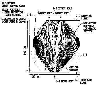
Figs. 5A-5C are diagrams illustrating a basic
concept and basic structure of the wave transmission
medium in accordance with the present invention. First,
technical terms will be described with reference to Fig.
5A. The reference numeral 1 of Fig. 5A designates an
optical circuit substrate, and 1-1 designates a design
region of an optical circuit comprising the wave
transmission medium in accordance with the present
invention. A first end face of the optical circuit
constitutes an incidence plane 2-1 onto which input light
3-l is launched. The input light 3-1 propagates through
the optical circuit, which is composed of the wave
transmission medium and has spatial refractive index
distribution, with repeating multiple scattering, and
is output from a second end face constituting an emitting
37
CA 02511944 2005-06-27
plane 2-2 as output light 3-2. It is assumed in the
present embodiment that the wave transmission medium
is composed of a dielectric, and that the spatial
refractive index distribution is implemented by setting
the local refractive indices of the dielectric
constituting the medium according to a theory that will
be described later.
The "field" (input field) formed by the input light
3-1 is modulated in accordance with the spatial
1o distribution of the refractive index of the wave
transmission medium constituting the optical circuit,
and is converted to the "field" (output field) formed
by the output light 3-2. In other words, the wave
transmission medium in accordance with the present
invention is an (electromagnetic) field converter for
correlating the input field with the output field
according to the spatial refractive index distribution.
As for the input field and output field, the optical
field in a cross section (cross section along the x axis
of Fig. 5A) perpendicular to the propagation direction
(the direction of the z axis of Fig. 5A) in the optical
circuit is called a (forward) propagation image
(propagation field or propagation light) at the location
(x, z) (see, Fig. 5B) . The coordinates z in Fig. 5A are
coordinates in the propagation direction of light, where
z = 0 is the incidence plane and z = Ze is the emitting
plane. On the other hand, the coordinates x are
38
CA 02511944 2005-06-27
coordinates in the horizontal direction perpendicular
to the propagation direction of light.
The term "field" generally refers to an
electromagnetic field or vector potential field of the
electromagnetic field. The control of the
electromagnetic field in the present embodiment
corresponds to consider the spatial refractive index
distribution in the optical circuit, that is, the
distribution of the dielectric constant. Although the
dielectric constant is given by a tensor, its scalar
wave approximation using only one component of the
electromagnetic field usually gives a good
approximation because the transition between
polarization states is rather small. Accordingly, the
present specification handles the electromagnetic
field as a complex scalar wave. Since the optical
"state" includes an energy state (wavelength) and a
polarization state, using the "field" to represent the
optical state, it contains the optical wavelength and
polarization state at the same time.
As for the optical circuit that does not make any
amplification nor attenuation of the propagation light,
specifying the spatial distribution of the refractive
index determines the image of the input light 3-1 (input
field) corresponding to the image of the output light
3-2 (output field) uniquely except for the focus. Such
an optical field from the emitting plane 2-2 side to
39
CA 02511944 2005-06-27
the incidence plane 2-1 side is referred to as a reverse
propagation image (reverse propagation field or reverse
propagation light) (see, Fig. 5C). Such a reverse
propagation image can be defined for each location in
the optical circuit. In other words, when considering
the optical field at an arbitrary location in the optical
circuit, it is possible to assume the reverse propagation
image for the image of the output light 3-2 at that
location by considering the location as a virtual
1o starting point of the "input light" . In this way, the
reverse propagation image can be defined for each
location of the optical circuit. As fora single optical
circuit, in particular, if the emitted field constitutes
the propagation field of the incident field, the
propagation field agrees with the reverse propagation
field at any points of the optical circuit.
Incidentally, although the field is usually a function
defined on the entire target space, the term "incident
field" or "emitted field" means a cross section of the
field on the incidence plane or emitting plane.
Likewise, as for the term "field distribution", when
a particular cross section is discussed, it means the
cross section of the field.
To explain a decision method of the refractive index
distribution, the following symbols are used to
represent individual quantities because the symbols
give better prospects. Here, since the light (field)
CA 02511944 2005-06-27
is not limited to single state light in the present
invention, the individual states are represented in
general by attaching affixes j to the light to represent
light composed of the superposition of light with a
plurality of states.
3(x): jth incident field (complex vector-valued
function, which is determined by the intensity
distribution and phase distribution specified on the
incidence plane, and by the wavelength and
polarization).
fi(x): jth emitted field (complex vector-valued
function, which is determined by the intensity
distribution and phase distribution specified on the
emitting plane, and by the wavelength and polarization).
As for ir' (x) and f3 (x) , the sum total of their optical
intensities is the same (or has only a negligible loss)
as long as no intensity amplification, wavelength
conversion or polarization conversion is carried out
in the circuit, and their wavelength and polarization
are the same. Consequently,
{ fir' ( x ) , f' (x) } : an input/output pair (a pair of the
input/output fields), which is determined by the
intensity distribution and phase distribution and by
the wavelength and polarization on the incidence plane
and emitting plane.
{nq } : refractive index distribution (a set of values
all over the optical circuit design region).
41
CA 02511944 2005-06-27
Since the optical field is determined when a set
of refractive index distributions is provided to the
given incident field and emitted field, it is necessary
to consider the field for the entire refractive index
distribution given by qth iterative calculation.
Although the entire refractive index distribution can
be represented by nq (x, z) , where (x, z) are indefinite
variables, it is represented by {nq } to distinguish it
from the value nq (x, z) of the refractive index at the
location (x, z).
nCOTe: a symbol representing a value of the
refractive index of a region such as a core of an optical
waveguide, which is higher than the refractive index
in the surroundings.
nclad: a symbol representing a value of the
refractive index of a region such as a cladding of an
optical waveguide, which is lower than ncore=
jil ( z , x, {nq }) : the value of the field at the location
(x, z) when the jth incident field 4j(x) propagates
through the refractive index distribution {nq} to Z.
f' (z, x, { nq }) : the value of the field at the location
(x, z) when the jth emitted field fi(x) reversely
propagates through the refractive index distribution
{nq} to Z-
The decision method of the refractive index
distribution in the present embodiment provides a method
of obtaining such {nq } that can implement the state in
42
CA 02511944 2005-06-27
which * (ze , x, {nq }) = fJ (x) holds for all j or a state
close to that state.
The terms "input port" and "output port" mean a
"region" in which the fields on the incident end face
and emitted end face are concentrated, and to which an
optical fiber can be connected to enable the optical
intensity to propagate through the fiber. As for the
intensity distribution and phase distribution of the
field, it is possible to design such that the jth and
to kth of them have different values. Thus, the incident
end face and emitted end face can each include a plurality
of ports. Furthermore, considering a pair of the
incident field and emitted field, the phase caused by
the propagation between them can vary depending on the
optical frequencies. Accordingly, as for the light
with different frequencies, that is, the light with
different wavelengths, it is possible to establish
different ports regardless of whether the field profile
including the phase is identical or perpendicular to
each other. As for the symbols, capital letters A, B,
C, ... are assigned to the incident port side, and small
letters a, b, c, ... are assigned to the emitting port
side.
Other letters such as a, y, g and w are appropriate
coefficients for numerical calculations, and the orders
of magnitude of them will be mentioned in the following
description. For example, they are subjected to fine
43
CA 02511944 2005-06-27
adjustment in actual numerical calculations according
to "Discussion on scheme stability" used in ordinary
numerical hydrodynamics.
The propagation direction is represented by z, and
the direction perpendicular to the propagation
direction is represented by x. The value z is zero on
the incidence plane 2-1 and ze on the emitting plane
2-2. As will be described later, sequential numbers
are assigned to distinguishable optical states of
interest. In this case, the jth incident field and the
desired emitted field corresponding to it are designated
by *' (x) and fJ (x), respectively. It is assumed here
that the electromagnetic field is a real number
vector-valued field, and has the wavelength
polarization state as parameters. The components of
the electromagnetic field are represented by a complex
number that can be handled easily mathematically to
denote the roots of the electromagnetic waves. In
addition, it is assumed in the following calculations
that the intensity of the entire field is normalized
to one. The j th incident field and emitted field mean
optical pair components that are sequentially numbered
and have attributes distinguishable by the intensity
distribution and phase distribution of the field, or
by the wavelength or polarization.
As illustrated in Figs. 5B and 5C, concerning the
jth incident field fir' (x) and output field f' (x) , the
44
CA 02511944 2005-06-27
propagation field and reverse propagation field are
denoted by 4r' (z, x, {n}) and f' (z, x, {n}) as complex
vector-valued functions of the location. Since the
values of the functions vary depending on the refractive
index distribution {n}, the refractive index
distribution (n) becomes a parameter. According to the
definition of the symbols, ijr' (x) = 4r' (0, x, { n j) , and
f'(x) = f'(ze, x, {n}). The values of the functions
can be easily calculated by a known method such as a
io beam propagation method when the incident field (x) ,
emitted field f3 (x) and refractive index distribution
{n} are given. The behavior of the individual fields
will be described below by way of example of more concrete
example.
Fig. 6 is a diagram illustrating a configuration
of a conventional arrayed waveguide grating circuit.
In the optical circuit design region 1-1, are formed
arrayed waveguides 5 between two star couplers (optical
multi/demultiplexers) 4-1 and 4-2 and a wave plate 6
inserted into the center of the arrayed waveguides 5.
Consider a 1xN wavelength demultiplexer in the
wavelength division multiplexing communication as
illustrated in Fig. 6, where N is the number of the
wavelengths. For example, consider a case where N
different signals, which have incident fields with
substantially equal field intensity and phase
distribution, and have numbered wavelengths Al , A2 , A3 ,
CA 02511944 2005-06-27
and AN, are launched into a single input port 3-1,
and the light with the jth wavelength is output from
a desired output port 3-2. In this case, to demultiplex
the light, it is necessary for the optical intensity
and phase distribution of the jth wavelength on the cross
section of the emitting plane of the waveguide to have
an independent emitted field pattern, which is called
a jth emitted field. Consider the case where the
demultiplexed light is output from the optical fiber.
In this case, the field patterns to be output consist
of a set of fields , in which the independent individual
emitted fields have spatially different locations.
Incidentally, to configure an optical circuit for
outputting a given set of incident fields at desired
emitted fields, the pattern of the incident fields or
emitted fields may have the same intensity and phase
distribution at the jth and kth wavelengths.
A general algorithm for determining the spatial
refractive index distribution will be described below.
Fig. 7 is a flowchart illustrating a calculation
procedure of determining the spatial refractive index
distribution of the wave transmission medium in
accordance with the present invention. Since the
calculation is carried out repeatedly, the number of
repetitions is denoted by q. Fig. 7 illustrates the
procedure of the qth calculation carried out when the
calculation up to the (q-1)th calculations have been
46
CA 02511944 2005-06-27
completed.
From the refractive index distribution {nq_1}
obtained by the (q-l)th calculation, the propagation
field and reverse propagation field as to the jth
incident field *'(x) and emitted field f'(x) are
calculated by the numerical calculations, and the
results are denoted as *'(z, x, {nq_1}) and f'(z, x,
{nq_1}), respectively (step S220).
Then, the refractive indices nq (z, x) at individual
locations (z, x) are calculated from the results by the
following expression (step S240).
nq(z, x) = nq_1(z, x)
- aSi Im[f'(z, x, {nq_1})*=~Jj(z, x, {nq_1})]===(1)
where the symbol in the second term on the right
side denotes an inner product, and Im[] denotes the
imaginary part of the result of the field inner product
within the brackets []. In addition, the symbol "*"
denotes a complex conjugate. The coefficient a is a
value obtained by dividing a number less than a fraction
of nq (z, x) by the number of sets of the field, which
is a positive small value. The symbol Sj denotes the
sum with respect to the affix j.
If the absolute value of the difference between
the valueir' (ze , x, {n}) of the propagation field on the
emitting plane and the emitted field f3 (x) becomes less
47
CA 02511944 2005-06-27
than a desired error dj by repeating the steps S220 and
S240 (YES at step S230), the calculations are completed.
The ground for obtaining the refractive index nq (Z,
x) according to the foregoing expression (1) is as
follows, which corresponds to calculating the
refractive index distribution by the steepest descent
method.
First, in order to minimize the difference between
the field Ir' (ze, x, {nq_1}) resulting from the incident
light propagating through the refractive index
distribution {nq_1} and the finally desired output f3 (x) ,
the residual R = Si f1(x) - iIr'(ze, x, {nq_1}) I2 must be
minimized, where f3 (x) or the like represents a function
of x rather than a coordinate of a particular x. Although
the individual pairs can be assigned different weights,
the same weight is used to calculate the sum for
simplicity's sake.
Here, a superposable region of the optical fields
is considered, and the inner product is defined by the
overlap integral of the field. The superposition of
the optical fields has finite energy, and the field to
be handled is limited to a spatially finite range.
Accordingly, the field mentioned here constitutes a
Hilbert space, and the optical propagation is defined
by a unitary transformation having the following
properties.
More specifically, the following expression holds:
48
CA 02511944 2005-06-27
*I (z, x, {nq-1}) = U(Z, Z0, {nq-1}) 1 (Z0, X, {nq-1}) ..
(2)
where U is a unitary operator from zo to z. If it is
assumed here that the reflection is negligible, the
following expression is obtained because of the
additivity of the propagation process.
U(z, z0, {nq_1}) = U(z, Z1, {nq_1})U(zl, Z0, {nq_1})
(3)
Furthermore, because it has unitarity f or the inner
product defined by the overlap integral, the following
expression holds:
U(z, zo, {nq_1})*U(z, z0, {nq_1})
= U(z, zo, {nq_1})-1U(z, Zo, {nq-1})
= IU(z, zo, {nq-1}) I2 = 1 ...(4)
where U(z, zo, {nq_1})* is a self-adjoint operator of
the operator U(z, zo, {nq-1}) , and U(z, zo, {nq_1})-1 is
an inverse operator of U (z , zo, { nq_1 }) , that is, an
operator that gives propagation in the reverse
direction.
Within a range where the difference I z' - z I between
z' an z is small enough, U (z ' , z, { nq_1 }) can be considered
49
CA 02511944 2005-06-27
as a matrix that provides transformation of just one
step in the beam propagation method, and U(z, z0, (nq-1})
and the like can be considered to be obtained by dividing
the propagation direction appropriately and by
repeating the operation.
Rewriting the residual R using the foregoing results
gives:
R = S1 I f'(x) - U(ze, Z' , {nq-1) )U(z' , 0, {nq-i}) '(x) 1 2
= SjIU(Ze, Z', {nq-1}) I2IU(Ze, Z' , {nq-1}) if7(x)
- U(Z' , 0, {nq-1})4J (X) I2
= S,IU(ze, Z', {nq-1}) - lfj(x)
- U(z', z, {nq-1) )U(Z, 0, {nq-1})4''(x) 1 2
= S If3(z', x, {nq_1})
- U(z' , z, {nq-i})4''(Z, x, {nq-1}) I2 =.. (5)
The variation (d,U(z' , z, {nq-1})) of U(z' , z, {nq_1})
at a particular location x on the x coordinate has the
following relationship with the variation (dõnq_i (Z, x) )
of nq_i (Z , x) at the particular location x on the x
coordinate at the limit of I z ' - z I ~O .
d,{U(z', z, {nq-i}) = -ixdxnq_1(Z, x)===(6)
where K is a positive coefficient with a value of an
order of the propagation constant in vacuum. Since it
is combined with other coefficients in the calculation,
CA 02511944 2005-06-27
it will not be described here in more detail.
From the foregoing results, the variation (dXR) of
the residual R at the particular location x on the x
coordinate, the following expression is obtained.
dXR = Sj{ - ixdnq-1(z, x)f'(z' , x, {nq-1})%'(z, x,
{nq-1})+c.c. }
2Kdnq-1(z, x)Im[Sjf'(z' , x, {nq-1)) *1jJJ(z, x,
{nq-1}) I
... (7)
In this case, if the following expression holds,
dnq-1(z, x) aIm[Sjf(z' , x, {nq-.1 })*lr'(z, x,
{nq-1}) I (a>O) ... (8)
dXR < 0 is obtained, which means that the variation in
this direction leads toward a local minimum. This is
the reason for varying the refractive index distribution
in the direction of the foregoing expression (1).
In the foregoing calculation, the initial value
{no) of the refractive index distribution can be set
at an appropriate value. However, the closer the
initial value {no} to the expected refractive index
distribution, the faster the calculation converges
(step S200). Furthermore, as for the calculation of
f ( z, x, { nq - 1 } ) and iIr' ( z, x, { nq - 1 }) for the individual
51
CA 02511944 2005-06-27
j, a computer capable of carrying out parallel
calculations can calculate them for each j (for each
f' ( z, x, {nq _ 1 } ) and ( z, x, { nq thereby being
able to improve the efficiency of the calculation using
a cluster system or the like (step S220). In addition,
when the computer includes a comparatively small memory,
it can select appropriate affixes j for the individual
q in the sum with respect to j in the foregoing expression
( 1 ) , calculate only f' ( z, x, {nq _ 1 } ) and fir' ( z, x, {nq _ 1 } )
io only for the affixes j selected, and repeat the
subsequent calculations (step S220).
In the operation above, if the value f' (z, x, {nq _ 1 } )
and the value fir' (z, x, { nq - 1 }) are close to each other,
the term Im[f'(z, x, {nq_1})* **j (Z, x, {nq_1})] in
expression (1) takes a value corresponding to the phase
difference so that reducing its value can provide the
desired output.
Fig. 8 is a diagram illustrating the behavior of
a field in the wave transmission medium to facilitate
understanding of the above-mentioned calculation
procedure. At any given position (x, z) in the optical
circuit design region 1-1 composed of the wave
transmission medium in accordance with the present
invention, a minute region is assumed which is
substantially parallel to the wavefront of the
propagating light, and has a substantially negligible
width (Az) . The cross section of the minute region is
52
CA 02511944 2005-06-27
called X. The term "substantially negligible width"
ref ers to such a distance that when the light propagates
across the distance Oz through the medium without the
refractive index distribution, the propagation light
has substantially the same phase as that of the previous
wavefront. The cross section X constitutes an
interface between an A circuit and a B circuit, where
the A circuit is an optical circuit on the side of the
incidence plane 2-1 with respect to the cross section
1o X, and the B circuit is an optical circuit on the side
of the emitting plane 2-2.
Consider desired sets of input/outputs, and assume
that the individual sets are each assigned a number from
j = 1 to N, and jth set has the incident field 4r' (x)
and emitted field f' (x) . When the incident field *1 (x)
is input to the A circuit and transmitted through the
circuit, the sum of the individual fields of the guided
wave, diffraction wave and scattered wave at the
interface Xis the field fir' ( z x , x, {nq }) . In addition,
as for the emitted field f' (x) propagating through the
B circuit in the opposite direction as the optical phase
conjugate of the light propagating through the A circuit,
the sum of the fields of the guided wave, diffraction
wave and scattered wave of the emitted field f3 (x) is
the field f'(zx + Oz, x, {nq}). Subsequently, the
average value (or weighted average value) P of the phase
differences between the field lIJ' (zx, x, {nq }) and the
53
CA 02511944 2005-06-27
field fj (zx + LXz, x, {nq }) are calculated for the
individual sets, and the refractive index distribution
on the interface X is determined such that the phase
difference P is canceled as much as possible in the range
of the desired refractive index. Since such refractive
index distribution is determined for each interface X,
the refractive index distribution of the entire wave
transmission medium can be determined by carrying out
the operation with varying the position of the interface
to X from zero (incidence plane) to ze (emitting plane)
on the z axis.
The determination of the spatial distribution of
refractive index in accordance with the present
invention can be expressed in different words that it
covers the wave transmission medium with a virtual mesh,
and decides the refractive index for each minute region
(pixel) provided by the mesh. Although such local
refractive indices can each take a desired value location
by location in principle, the simplest system consists
of pixels with a low refractive index (nL) and pixels
with a high refractive index (nH), and the spatial
distribution of the two types of the pixels decides the
entire refractive index distribution. In this case,
it is possible to consider the locations in which the
low refractive index pixels in the medium are present
as the interstices of the high refractive index pixels,
or reversely to consider the locations in which the high
54
CA 02511944 2005-06-27
refractive index pixels in the medium are present as
the interstices of the low refractive index pixels. In
other words, the wave transmission medium in accordance
with the present invention can be expressed as the medium
with a uniform refractive index, the desired locations
(pixels) of which are replaced by the pixels with
different refractive index.
The operation for deciding the refractive index
distribution described above is summarized as follows.
The medium (dielectric in the case of light) enabling
the holographic wave transmission is provided with an
input port and output port, and the numerical
calculations are used to obtain the field distribution
1 of the propagation light that is launched into the
input port (forward propagation light) and the field
distribution 2 of the phase conjugate light (reverse
propagation light). The reverse propagation light is
achieved by reversely transmitting from the output port
side the output field that is expected to be output when
the optical signal launched into the input port is output
from the output port. Then, the spatial refractive
index distribution in the medium is obtained from the
field distributions 1 and 2 such that the phase
difference between the propagation light and the reverse
propagation light is canceled at individual points (x,
z). Employing the steepest descent method as a method
of calculating the refractive index distribution can
CA 02511944 2005-06-27
reduce the difference between the two fields by varying
the refractive index according to expression (1) by
varying the refractive index in the direction obtained
by the steepest descent method using the refractive
indices of the individual points as variables. Then,
applying such a wave transmission medium to an optical
component that emits the light launched into the input
port from a desired output port can increase the
effective optical path length by the interference due
to the multiple scattering caused between the
propagating waves in the medium, thereby being able to
configure an optical circuit with high optical signal
controllability even with mild refractive index
variation (distribution).
Optical circuits configured using the foregoing
wave transmission medium will now be described below
by way of embodiments. Unless otherwise noted, it is
assumed in the following embodiments that optical
circuits have the same refractive index distribution
as a silica-based buried optical waveguide formed on
a substrate in the vertical direction of the substrate,
and that the thickness of the optical circuit (layer
thickness) is approximately equal to that of the single
mode optical waveguide. Furthermore, the substrate
consists of a silicon substrate. Then, a layer, the
refractive index of which is regulated by adding dopants
to the silica, is deposited on the substrate, and the
56
CA 02511944 2005-06-27
pattern of the optical circuit is formed by the
microprocessing used in the fabrication process of the
semiconductor. Thus, the pattern of the optical
circuit is two-dimensional, and is formed in the
horizontal direction of the substrate.to achieve the
function of the optical circuit.
However, when the circuit, which includes the high
refractive index section and low refractive index
section, is formed on the substrate two-dimensionally,
1o and if the low refractive index section is simply assumed
to have no region corresponding to the core of the optical
waveguide, a loss occurs in the optical circuit.
Accordingly, it need scarcely be said that the optical
circuit must be designed considering the vertical
direction of the substrate even though the optical
circuit itself is two-dimensional.
As described above, the optical circuit in
accordance with the present invention is fabricated by
applying the semiconductor microprocessing.
Accordingly, the refractive index distribution of the
optical circuit has a binary pattern unless otherwise
noted. In the pattern on the substrate, a region with
a high refractive index is called a high refractive index
section, and a region with a low refractive index is
called a low refractive index section. In addition,
since the refractive index variation is given by the
deposition of the layer whose refractive index is
57
CA 02511944 2005-06-27
regulated, a region with a high refractive index in the
vertical direction of the substrate is referred to as
a high refractive index layer, and a region with a low
refractive index is called a low refractive index layer.
In the case where no special problem is present, the
high refractive index section is called a "core ", and
the low refractive index section is called a "cladding"
in accordance with the custom of the optical waveguide
structure. Furthermore, to discuss a pattern in a
horizontal plane on the substrate, the basic unit of
the pattern is called a "pixel", and a set of the "pixels"
combined in a block constitutes a macro pattern. In
the simplest case, the pixels are placed on periodic
lattice points with a pixel size which are determined
by a virtual mesh, and the high refractive index section
and the low refractive index section constitute the
pattern. It is not necessary, however, to place the
pixels on the lattice points. For example, they can
be placed intentionally on points displaced from the
lattice points to achieve the desired refractive index
distribution.
[EMBODIMENT 1]
As for the so-called step-index optical circuit,
it is not self-evident as to whether an optical circuit
can be designed according to the foregoing expression
(1) because the value the refractive index can take is
58
CA 02511944 2005-06-27
limited. However, even in the case where the value the
refractive index can take is limited, it is possible
to adjust the optical phase globally by repeating
adjustment of the local refractive indices. Therefore
it is possible to design the optical circuit by assuming
a steplike refractive index distribution that has an
upper limit of the refractive index of the dielectric
constituting the optical circuit and a finite number
of refractive indices reaching the upper limit, and by
calculating the refractive index distribution of the
optical circuit using the refractive indices as a limit
value. The present embodiment designs the optical
circuit based on such an idea.
In the present embodiment, the idea is applied to
an optical waveguide that has the same structure as a
step-index planar optical waveguide, and has a structure
in which the core of the waveguide is patterned in dots
in the optical circuit design region. Thus, a
wavelength division filter of 1.31 pm and 1.55 pm was
designed.
The present embodiment supposes a silica optical
waveguide. In addition, it is assumed in the
calculation of the spatial distribution of refractive
index that only two types of refractive indices--the
refractive index of the core (high refractive index
section) and the refractive index of the cladding (low
refractive index section) --are considered, and that the
59
CA 02511944 2005-06-27
refractive index distribution is calculated which is
obtained by distributing the two types of the refractive
indices in the optical circuit design region.
Furthermore, although it is assumed that the
refractive index values which are the parameters can
take any values in the algorithm of computing the
refractive index distribution described in connection
with Fig. 7, the present embodiment obtains the
refractive indices here by calculating values vq
1o according to the following expression (9), and by
applying the following expressions (10) and (11) to the
values vq.
Vq(Z, X) = Vq_1(Z, X)
- aSj Im[f'(z, x, {nq_1})*=iJs'(z, x, {nq_1})]
... (9)
nq (Z, X) = ncore when Vq (Z, X) > (ncore + nclad)/2,
and
(10)
nq(Z, X) = ncladd when Vq(Z, x) < (ncore + nclad)/2
... (11)
where ncore is the refractive index corresponding to
the core, and nc 1 a d is the refractive index corresponding
to the cladding. Consequently, the refractive index
distribution in the optical circuit design region is
achieved by spatially distributing the two types of the
CA 02511944 2005-06-27
refractive indices. Generally, the relationship ncore
nc 1 a d holds. Even such calculation enables the design
of the optical waveguide that can produce a desired
optical output enough as will be described below.
Furthermore, for simplicity's sake, the calculation is
carried out by considering that the refractive index
(nc o r e) corresponding to the core pattern among the two
types of the refractive indices is an effective
refractive index, and that both the propagation
1o direction and the lateral direction are each one
dimensional.
Figs. 9A and 9B diagrams illustrating setups in
the optical circuit design in the present embodiment.
First, it is assumed that polarization multiplexed light
launched into an input port 3-1 is output from an output
port 3-2. Then by adjusting the refractive index
distribution, are established a pair of incident field
i1 (x) and emitted field fl(x) with the wavelength of
1.31 um (that is, j = 1 in terms of the foregoing symbol)
as illustrated in Fig. 9A, and a pair of incident field
*2(x) and emitted field f2(x) with the wavelength of
1.55 um (that is, j = 2 in terms of the foregoing symbol)
as illustrated in Fig. 9B. Although the fields are
defined all over the incidence plane 2-1 and emitting
plane 2-2, only regions at which the field intensity
is concentrated are illustrated in Figs. 9A and 9B . Such
a pair of incident/emitted fields {ir3 (x) , f' (x)) are
61
CA 02511944 2005-06-27
referred to as an input/output pair from now on.
Figs. 10A and 10B are diagrams illustrating the
refractive index distribution (Fig. 10A) and
transmission spectra (Fig. 10B) in the present
embodiment 1. By repeating the foregoing algorithm of
calculating the refractive indices about 200 times, the
optical circuit with the refractive index distribution
as illustrated in Fig. 10A is obtained. Here, black
regions 1-11 in the optical circuit design region 1-1
of Fig. 10A are the high refractive index section
(dielectric multiple scattering section) corresponding
to the core, and regions other than the black regions
are the low refractive index section corresponding to
the cladding. The refractive index of the cladding is
assumed to be equal to that of the silica glass, and
the refractive index of the core is assumed to be higher
than that of the silica glass by 1.5%. The optical
circuit is 300 pm long by 140 pm wide.
The mesh used for calculating the refractive index
distribution has140x300(=42000)cells. Accordingly,
the number of parameters of the refractive index
distribution is 42000, and the parameters must be
optimized. If the parameters are to be optimized by
obtaining one numerical differentiation for each of the
parameters by simply applying the steepest descent
method, it is necessary to calculate 42000 propagations
of light for each step calculation. In contrast with
62
CA 02511944 2005-06-27
this, the present embodiment can complete the
calculation by computing the optical propagation twice,
thereby enabling the design of the optical circuit in
a short time presenting no problem in practice.
Fig. 10B illustrates the transmission spectra of
the optical circuit thus designed. It illustrates the
characteristics of light with the wavelength of 1.31
um which is output from an output port a, and of light
with the wavelength of 1.55 pm which is output from an
output port b. In other words, it is seen that the
demultiplexer is formed in terms of the wavelength.
Incidentally, the input and output directions of the
light as shown in Figs. 9A and 9B can be reversed so
that the waves with the two wavelengths are launched
into the output ports a and b, multiplexed, and output
from the incidence planet - i. Accordingly, the optical
circuit can operate asa multiplexer. Thus, the optical
circuit described in the present embodiment can operate
as the multi/demultiplexer in terms of the optical
wavelength.
To secure the function of the optical circuit, the
light propagating through optical circuit must be
sufficiently confined within the optical circuit. As
for the refractive index distribution as illustrated
in Fig. 10A, the core, that is, the high refractive index
section is distributed in dots in the optical circuit
design region, thereby causing concern that the optical
63
CA 02511944 2005-06-27
confinement in the thickness direction of the substrate
can become insufficient.
In view of this, the optical circuit is assumed
to have a structure in which the high refractive index
section is composed of two high refractive index sections
(first high refractive index section and second high
refractive index section) , and the high refractive index
sections are sandwiched between low refractive index
sections from its top and bottom. Then, the refractive
index distribution of the optical circuit is calculated.
Fig. 11A is a schematic cross-sectional view of
an optical circuit that has a planar optical wave
circuit-like refractive index distribution, and can
carry out the optical confinement in the direction
perpendicular to the substrate. The high refractive
index section 1-11 of the optical circuit is composed
of the two high refractive index sections (first high
refractive index section 1-11a and second high
refractive index section 1-lib), and the second high
refractive index section 1-llb has a refractive index
greater than the first high refractive index section
1-11a. The high refractive index section 1-11 is
sandwiched between the low refractive index sections
1-12 at the top and bottom, thereby configuring the
optical circuit. In the optical circuit, the second
high refractive index section 1-11b acts as the so-called
core", whereas the first high refractive index section
64
CA 02511944 2005-06-27
1-11a is provided to confine the light propagating
through the core in the thickness direction of the
substrate (direction perpendicular to the substrate).
In Fig. 11A, the calculations are made by assuming that
the refractive index difference between the low
refractive index section 1-12 and the first high
refractive index section 1-lla, and the refractive index
difference between the first high refractive index
section 1-11a and the second high refractive index
section 1-lib are each 1.5%. At the right-hand side
of Fig. 11A, an effective refractive index profile of
the optical circuit in the vertical direction is shown,
and at the bottom of Fig. 11A, an effective refractive
index profile of the high refractive index section 1-11
in the horizontal direction is shown.
The optical circuit with such a structure can easily
carry out the optical confinement in the thickness
direction of the substrate by the first high refractive
index section 1-11a provided around the second high
refractive index section 1-1ib constituting the core.
When providing the optical circuit with the optical
input/output sections, two cases are possible: a first
case has the first high refractive index section 1-11a
guide the light (Fig. 11B); and a second case has the
second high refractive index section 1-1ib guide the
light (Fig. 11C). In addition, the optical coupling
with optical fibers can be optimized by adjusting the
CA 02511944 2005-06-27
field radius by optimizing the shapes of the first high
refractive index section 1-11a and second high
refractive index section 1-lib and by combining them.
Since the output field is calculated in a complex
number, the phase of the output field can also be obtained.
Consequently, the foregoing calculation procedure of
the optical field is also applicable to the case where
the optical phase adjustment is necessary such as
fabricating an external resonator laser by combining
1o the foregoing optical circuit with a semiconductor
optical amplifier provided with an antireflection
coating.
Although the beam propagation method is used to
calculate the foregoing optical fields, this is not
essential. For example, a finite difference
time-domain method (FDTD) can be used when the memory
capacity for the computer used for the operation is
enough. Generally speaking, since the beam propagation
method calculates the optical output in a linear
direction, the position of the output port is limited.
For example, the present embodiment employs the plane
opposite to the incidence plane as the emitting plane.
In contrast with this, since the calculation using the
finite difference time-domain method enables the
position of the output port to be selected flexibly,
it is not difficult to design an optical circuit
including an optical path with a sharp bending. This
66
CA 02511944 2005-06-27
holds true for the following embodiments. In addition,
to implement such a circuit by combining directional
couplers, even only the directional coupler region
requires an optical circuit region of a few hundred
micrometers long. In contrast with this, the foregoing
method can construct the optical circuit with a size
of a fraction of that, thereby being able to miniaturize
the optical circuit.
[EMBODIMENT 21
The present embodiment designs the same optical
circuit as that of the embodiment 1 in accordance with
the following calculation method of the refractive index
distribution. The outline of the optical circuit will
be briefly described with reference to Fig. 5, again.
First, an arbitrary refractive index distribution {n}
is given, and the field distribution 1, fir' (z, x, {n}),
of the input light corresponding to the distribution
{n} is calculated. Then, the reverse propagation light
(field distribution 2, f1 (z, x, {n})) with the field
expected to be output from the output port as the output
light is successively calculated by virtually
transmitting the reverse propagation light toward the
incidence plane 2-1.
Take an example of Fig. 8. First, the refractive
index distribution is changed such that the phase of
the cross section ' (zx, x, {n}) of the field distribution
67
CA 02511944 2005-06-27
1 at a location z = zX matches the phase of the cross
section f' (zx + Az, x, {n)) of the field distribution
2 at that location. Second, using the refractive index
distribution after the change, the cross section f3 (z,
x, {n)) (z = zX + Oz to zX) of the field distribution
2 is recalculated from (zx + Oz) to zX. Then, the same
operation is successively repeated after placing (zx
- Oz) at z, . At the time when the cross section of the
field distribution 2 reaches the incidence plane 2-1,
the cross section of the field distribution 1 of the
input light is reversely transmitted in the propagation
direction virtually. Then, matching the phase of the
cross section of the field distribution 1 to that of
the cross section of the field distribution 2, the
refractive index distribution is successively decided.
The calculation is carried out until the cross section
of the field distribution 1 arrives at the emitting plane
2-2.
The procedure, which constitutes one routine, is
repeated so that the refractive index distribution is
calculated successively with transmitting the field
distribution 2 and field distribution 1 alternately in
the reverse and forward directions. The foregoing
calculation is repeated until the error between the
desired emitted field and the emitted field f' (x) , which
is output when the incident field ilr' reaches the emitting
plane 2-2, becomes less than a desired error.
68
CA 02511944 2005-06-27
As will be described later, the procedure can reduce
the time period required for the design of the optical
circuit, thereby enabling the design of a large-scale
optical circuit in practical time and effort.
First, the algorithm will be described.
Fig. 12 is a flowchart illustrating a general flow
of the optical circuit design of the present embodiment
2. Using the same symbols as those of expression (1) ,
the following expressions are obtained.
nq (z + dz, x)
_ -yS;arg[f'(z + dz, x, {nq_1))*=4r'(z, x, {nq})]
nq+1(z - dz, x)
= -ySjarg[f' (z, x, {nq+1 })* =11r' (z - dz, x, {nq}) ]
...(1")
where the coefficient y is obtained by dividing a value
of an order of (2ko dz) - 1 by the number of input/output
pairs, and ko is the wave number in vacuum, which is
on the order of the average wave number of the input
signal considered here. The wave number "on the order"
means that there are variations on the order of the
relative effective refractive index.
The foregoing expressions (1 ') and (1") mean that
the term ImS;f'(z', x, {nq_1})*i1s'(z, x, {nq_1}) of
expression (1) has no phase difference at a local minimum
69
CA 02511944 2005-06-27
point, and that the refractive indices are placed
according to this f act so that the term arg [ f' (z' , x,
{nq_1}) *j (z , x, {nq_1 }) ] is reduced. In particular, when
the phase difference is small, since the term ImSjf (z' ,
x, {nq_1 }) *1IJJ (z , x, { nq_1 }) becomes equivalent to the term
arg[fj(z' , x, {nq_1})*IJJ(z, x, {nq_1}) ] except for the
amplitude, theterm arg[f'(z' , x, {nq_1})*'(z, x, {nq_1}) ]
can be replaced by ImSjf3(z' , x, {nq_1})*lr'(z, x, {nq_1}),
which corresponds to changing the refractive index by
io weighting it with the intensity of the field of each
location. In the following description arg [ f' (z' , x,
{nq_1})*Jr'(z, x, {nq_1})] is used for simplicity's sake.
Expression (1') means that when f'(z, x, {nq_1})
is given in the entire region, the term is ( z, x, {nq } )
is calculated from nq (z , x) obtained (step S670), and
that nq (z + dz, x) at the point (z + dz) , the coordinate
z plus the minute distance dz, is determined from i4s (z,
x, {nq }) (step S680) (step S655). Here, the symbol " = "
represents the inner product operation, arg[]
represents its argument, and the symbol "*" denotes the
complex conjugate.
Expression (1") means that when (z, x, {nq }) is
} )
given in the entire region, the term f i (z, x, { nq +I
is calculated from nq+1 (z, x) obtained (step S620), and
that nq +I (z - dz, x) at the point (z - dz) , the coordinate
z minus the minute dz, is obtained (step S630) (step
S605).
CA 02511944 2005-06-27
By repeating the computation of expression (1')
(step S655) and the computation of expression (1") (step
S605) alternately (step S697), the calculation of the
refractive index distribution is carried out until the
calculation is completed (YES at step S695).
In the calculation of the present embodiment, the
phase matching is established between the cross section
of the field distribution 1 and the cross section of
the field distribution 2 in the minute distance dz, which
1o will cause oscillation with a short period in the actual
calculation, thereby bringing about considerably large
calculation error. Considering this, the coefficient
y is multiplied by an arbitrary rare number g so that
their product (g=y) becomes less than a fraction of
(2k0 dz) - 1 . In addition, as for the position of the field,
it need not accord with z + dz completely, but take an
intermediate value, or it may agree with a position (z
+ wdz) (0 s w s 2) at which nq (z + dz, x) takes the center
value of the refractive indices at the location z and
location z + 2dz. By such handling, the foregoing
expressions (1') and (1") are revised as follows.
nq(z + dz, x) = (1-g)nq_1(z + dz, x)
- gySjarg[fj (z + wdz, x, {nq_1 })* 'Ir' (z, x,
{nq }) ]
nq+1(z - dz, x) _ (1-g)nq(z - dz, x)
71
CA 02511944 2005-06-27
- gySjarg[f' ( z , x, {nq+l })* =~r' (z - wdz, x,
{nq})l
Thus, the short periodic oscillation is prevented by
the weighted average using the rare number g in the range
0 < g s 1 as the parameter. In the present embodiment,
they are set at w = 1 and g = 0.25. In addition, the
refractive index distribution is assumed to be a
step-index type as in the embodiment 1, and is subjected
to the same discrete processing. The optical circuit
of the present embodiment is the same as that of the
embodiment 1.
To carry out the calculation according to the
algorithm, data about the previous fields are needed
as illustrated in Fig. 13A, and a large capacity of memory
is required to store the data on the fields previously
transmitted. For example, to calculate a 1000 pm x 1000
pm region using a mesh with a uniform pitch of 0.1 pm,
even a simple pair of fields requires 2 x 8 x 108 = 1. 6 Gbytes
in the form of complex number values representing
double-precision real number values, thereby making the
calculation difficult. The difficulty is circumvented
by enabling the memory to store only the wave front region
by utilizing a fact that propagating the once transmitted
field in the reverse direction as illustrated in Fig.
13B brings about the same state in which the field is
72
CA 02511944 2005-06-27
transmitted to an intermediate location.
More specifically, the calculation is carried out
using a memory for only two wavefronts as follows. First,
the field f' (z = 0, x, {nq_1}) , which results from
transmitting the output field in the reverse direction
as illustrated in Fig. 13C, is transmitted in the forward
direction as an initial value, thereby obtaining f(z,
x, { nq_1 } ; f'q_1) which is used as the value f' (z, x, { nq_1 }) .
Likewise, the field *j (z = Ze, x, {nq_1}) is transmitted
in the reverse direction as the initial value, thereby
obtaining g (z , x, { nq_1 } ; *'q_1) which is used as the value
fir' (z , x, { nq_1 }) . Thus, the memory for only two
wavefronts enables the calculation. The calculation
is performed as to the fields up to both the ends of
the calculation region as shown in the algorithm of Fig.
12. Thus, the calculation results can be transmitted
in the reverse direction as the initial values.
Although the method doubles the calculation amount, and
hence delays the calculation, it can be used properly
in isolation or together with the method that stores
the data once in the memory depending on the conditions.
Figs. 14A and 14B are graphs illustrating behavior
of the convergence of the calculations in the embodiments
1 and 2. Figs. 14A and 14B each illustrate transmittance
(dB) to the desired output port and crosstalk (dB) into
other output ports against the number of repetitions
of the calculations in the embodiments 1 and 2. The
73
CA 02511944 2005-06-27
numbers of repetitions of the calculations correspond
to the numbers of repetitions of the loop as illustrated
in Figs. 7 and 12, the calculation amounts of which are
substantially equal.
It is seen by comparing Fig. 14A with Fig. 14B that
although the calculation method the embodiment 1 employs
requires repetitions of about 200 times until the
convergence, the calculation method the embodiment 2
employs can converge the calculation by repetitions of
1o several times. In other words, the calculation method
of the embodiment 2 can converge the calculation several
tens of times faster than the calculation method of the
embodiment 1. Consequently, the calculation method of
the embodiment 2 is applicable to the design of a rather
large-scale optical circuit.
Figs. 15A and 15B are diagrams illustrating the
refractive index distribution (Fig. 15A) and
transmission spectra (Fig. 15B) of the optical circuit
in the present embodiment. As shown in Fig. 10B, the
transmission spectra of the optical circuit illustrate
the characteristics of light with a wavelength of 1.31
pm which is output from the output port a, and of light
with a wavelength of 1.55 pm which is output from the
output port b. In other words, it is seen that the
demultiplexer (and multiplexer) is formed in terms of
the wavelength.
As compared with the refractive index distribution
74
CA 02511944 2005-06-27
of the optical circuit of the embodiment 1 illustrated
in Fig. 10A, the refractive index distribution of the
optical circuit of the present embodiment illustrated
in Fig. 15A has a comparatively uniform distribution
of the high refractive index section 1-11. As a result,
the effective refractive index increases its uniformity,
thereby increasing the uniformity of the effective
refractive index in the thickness direction of the
substrate in the optical circuit design region 1-1, and
1o reducing the unevenness of the optical confinement in
that direction. In other words, it becomes possible
to prevent the optical scattering in the thickness
direction of the substrate. As a result, the single
high refractive index section 1-11 can by itself
implement the optical circuit capable of optical
confinement without setting up the refractive index
distribution using the pair of high refractive index
sections as illustrated in Fig. 11A.
In particular, setting the refractive indices of
the individual pixels of the mesh in a spatially random
distribution as the initial refractive index
distribution for calculating the refractive index
distribution, the final refractive index distribution
obtained by the calculation has a more random
distribution. Thus, the refractive index distribution
can be implemented which is suitable for the optical
circuit with the structure including only the single
CA 02511944 2005-06-27
high refractive index section.
[EMBODIMENT 3]
In the present embodiment, a design method will
be described of a wavelength division
multi/demultiplexing circuit for demultiplexing and/or
multiplexing four wavelengths 1.53 pm, 1.54 pm, 1.55
pm and 1.56 pm.
Figs. 16A and 16B are diagrams illustrating
condition settings for the optical circuit design of
the four-wavelength demultiplexer of the present
embodiment: Fig. 16A illustrates the case where only
a TE mode is set as the polarization state of the input
light; and Fig. 16B illustrates the case where a TM mode
in addition to the TE mode is set as the polarization
state of the input light.
First, in the case of setting only the TE mode,
wavelength division multiplexed light is input to the
input port 3-1, and optical waves with different
wavelengths are emitted from the individual ports of
the output port 3-2 as illustrated in Fig. 16A. The
incidence plane 2-1 includes one input port 3-1, and
the emitting plane 2-2 includes four ports a, b, c and
d. The light including the four wavelengths 1.53 pm,
1.54 pm, 1.55 pm and 1.56 pm multiplexed is launched
into the input port 3-1, and the optical waves with the
wavelengths 1.53 pm, 1.54 pm, 1.55 pm and 1.56 pm are
76
CA 02511944 2005-06-27
output from the port a, port b, port c and port d of
the output port 3-2. Accordingly, the combinations of
the fields for calculating the refractive index
distribution consist of the four combinations of the
multiplexed input light field with the optical fields
with the wavelengths of 1.53 pm, 1.54 pm, 1.55 pm and
1.56 pm output from the four output ports (a, b, c and
d).
Figs. 17A and 17B are graphs illustrating
io transmission loss spectra (transmittance (dB)) of the
optical circuit calculated in the present embodiment:
Fig. 17A is the case where only the TE mode is set as
the polarization state of the input light (corresponding
to the conditions of Fig. 16A) ; and Fig. 17B is the case
where the TM mode in addition to the TE mode is set as
the polarization state of the input light (corresponding
to the conditions of Fig. 16B).
The spectra of the optical waves emitted from the
output port 3-2 become as illustrated in Fig. 17A, when
the condition settings are made such that the field of
the input light has the TE mode as the polarization state
for the substrate 1. In Figs. 17A and 17B, the TE mode
is represented by bold lines, and the TM mode, the
polarization state normal to the TE mode, is represented
by thin lines. The reason for calculating the spectra
for each polarization state is that the effective
refractive index the light propagating through the
77
CA 02511944 2005-06-27
optical circuit undergoes is slightly different in the
TE mode and TM mode. Therefore, the present embodiment
carries out the design of the wavelength division
multiplexing demultiplexing circuit as follows. First,
the optical waves of the four wavelengths launched into
the input port 3-1 are each assumed to be polarization
multiplexed light having the TE mode and TM mode. Second,
the optical waves with the same wavelength but having
the TE mode light and TM mode, respectively, are output
from the same output port (a, b, c or d). Thus, the
total of eight input/output pairs are set by subdividing,
in accordance with the two polarization states, the four
pairs of the fields which are divided in terms of the
wavelengths, thereby adjusting refractive index
distribution (Fig. 16B).
The method can reduce the differences in the
transmission losses due to the difference in the
polarization states as illustrated in Fig. 17B.
Although not shown in a drawing, as a variation of the
design conditions illustrated Fig. 16B, it is possible
to adjust the refractive index distribution such that
the polarization multiplexed light launched into the
input port is output from different designated output
ports for the individual polarizations.
As described above, setting up the pairs of the
incident/emitted fields using the wavelengths and
polarization states as the parameters enables the
78
CA 02511944 2005-06-27
flexible design of a polarization-independent optical
circuit or polarization-dependent optical circuit. In
addition, using the birefringence of the substrate in
the calculation as a parameter can eliminate the
polarization-dependence.
To configure an optical circuit having equivalent
functions by using the conventional arrayed waveguide
grating including the silica-based optical waveguides,
even the star couplers alone must occupy an area of
several millimeters long to provide a sufficient number
of arrayed waveguides, and besides, the arrayed
waveguides must be bent. Accordingly, it is inevitable
that the size of the optical circuit becomes greater
than a few square millimeters (typically, greater than
one square centimeter). Furthermore, it is sometimes
necessary to insert a wave plate into the optical circuit
to eliminate the polarization-dependence. In contrast
with this, according to the optical circuit design of
the present embodiment, it is possible to configure an
optical circuit that is equivalent to the conventional
optical circuit in the functions, and has a size less
than one hundredth of the conventional circuit.
[EMBODIMENT 4]
The present embodiment is an example of configuring
an optical wavelength band transmission circuit.
Figs. 18A and 18B are diagrams illustrating
79
CA 02511944 2005-06-27
condition settings for the optical circuit design of
the present embodiment: Fig. 18A illustrates the case
where a plain bandpass filter is set; and Fig. 18B
illustrates the case where a dummy port for band shaping
is set. The total length of these optical circuits is
1500 pm.
In addition, Figs. 19A and 19B are graphs
illustrating spectra of transmission losses of the
output optical waves emitted from the output ports of
1o the optical circuit adjusted under the condition
settings as illustrated in Figs. 18A and 18B,
respectively.
In the condition settings illustrated in Fig. 18A,
the light including six wavelengths 1. 530 pm, 1. 535 pm,
1.540 pm, 1.550 pm, 1.555 pm and 1.560 pm is launched
into the input port 3-1 as the wavelength division
multiplexed light, and desired dispersion
characteristics are implemented by adjusting the phases
of the optical waves with the above-mentioned
wavelengths so that the two output ports (a and b) of
the output port 3-2, which are separated apart by 10
pm, produce 1.530-1.540 pm band light from the port a,
and 1.550-1.560 pm band light from the port b.
The present embodiment employs the calculation
method as described in the embodiment 2, and assumes
the same resolution and circuit scale as the embodiment
3. In this case, as illustrated in Figs. 17A and 17B,
CA 02511944 2005-06-27
the 3dB-attenuation wavelength bandwidth is about 5 nm
on one side when a pair of the fields is set for each
wavelength. Thus, the wavelength spacings are set at
nm, and are uniformly distributed across the
5 transmission band in which the six pairs of the fields
of the wavelengths are to be obtained. Although the
transmission loss spectra calculated by the foregoing
calculation method are substantially rectangular as
illustrated in Fig. 19A, the transmission in the shorter
1o wavelength region is not suppressedsufficiently. Thus,
as illustrated in Fig. 18B, another port (port c) is
provided on the output side with a spacing of 10 pm from
the port a. The port c is used as a band-shaping dummy
port, and the calculation is carried out under the
assumption that a set of optical signals with the
wavelengths of 1.510 pm, 1.515 pm and 1. 520 pm is output
from the dummy port.
The dummy port can produce the transmission spectra
as illustrated in Fig. 19B, which can suppress the
optical transmission sufficiently even in the shorter
wavelength region. As a result, the transmission
filter is implemented that enables the individual
spectra output from the port a and port b (and port c)
to take a rectangular shape.
[EMBODIMENT 5]
The present embodiment relates to a configuration
81
CA 02511944 2005-06-27
of an optical wavelength band transmission circuit as
the embodiment 4. The parameters such as the
wavelengths and size of the region differ from those
of the embodiment 4 (the total length of the optical
circuit is600pm). In addition, although the foregoing
embodiments 1-4 handle the input field and output fields
as the real number vector functions of the locations
(the positions in the optical circuit design region),
the present embodiment calculates them as complex number
io vector functions. More specifically, the present
embodiment carries out the condition settings in such
a manner that the optical circuit includes a plurality
of output ports (port a, port b and dummy port c), and
that when plane-wave-like fields (that is, fields with
uniform phase distribution) are to be produced from the
output ports, the optical waves (output fields) produced
from the adjacent output ports have different phases.
In other words, the fields output from the port a and
port b are set such that they have the same complex value,
but has different phases.
Figs. 20A and 20B are diagrams illustrating setting
conditions and spectra of the transmission losses of
the optical circuit of the present embodiment. As
illustrated in Fig. 20A, optical waves spaced 10 nm apart
(wavelength spacings of 10 nm) in a wavelength range
from 1.510 to 1.560 pm are launched into the input port
3-1, and the optical waves of 1.530 pm, 1.535 pm and
82
CA 02511944 2005-06-27
1. 540 pm are produced from the output port a, the optical
waves of 1.550 pm, 1.555 pm and 1.560 pm are produced
from the output port b, and the optical waves of 1.510
pm, 1.515 pm and 1.520 pm are produced from the dummy
port c. Incidentally, the port a and port b are spaced
7 pm apart, and the port a and dummy port c are spaced
pm apart.
It is further set that the optical waves launched
into the input port 3-1 have the phase difference of
10 zero with the optical waves output from the port a, and
the phase difference of p with the optical waves output
from the port b. In addition, the spacing between the
port a and port b is extremely narrowed to 7 pm. This
makes it possible to suppress the crosstalk of the light
to be output from the port a into the port b, or vice
versa. The reason for this is as follows. When the
optical waves output from the port a and port b have
the same phase difference with respect to the optical
waves launched into the input port 3-1, the crosstalk
wave and non-crosstalk wave have nearly the same phase
at the port a and port b. Accordingly, the crosstalk
waves are gathered just as the signal light, thereby
increasing the crosstalk. In contrast, when the
optical waves output from the port a and port b have
a phase difference with respect to the optical waves
launched into the input port 3-1 as in the present
embodiment, the crosstalk waves interfere with each
83
CA 02511944 2005-06-27
other, thereby preventing the crosstalk waves from being
gathered to the individual ports.
In Fig. 20B, solid lines represent spectra when
the phase difference between the fields output from the
port a and port b is p, and broken lines represent spectra
when the phase difference between the fields output from
the port a and port b is zero. As illustrated in Fig.
20B, both the cases can implement a transmission filter
that outputs rectangular optical spectra from the port
1o a and port b. However, the transmission filter that
has the phase difference p between the fields output
from the port a and port b can suppress the crosstalk
more and implement a sharper rectangular filter than
the transmission filter that has no phase difference
as described above.
The results of the present embodiment indicate that
the phase control of the output light is carried out
by only setting the phase parameters for the individual
channels. Since such phase relationships can be
established not only between the output ports, but also
between the input ports, the phase control between these
ports enables a Mach- Zehnder(MZ) interferometer or the
like to be configured by combining the present optical
circuit with other external waveguide circuits.
[EMBODIMENT 6]
Figs. 21A-21D are diagrams illustrating a setup
84
CA 02511944 2005-06-27
of the input/output pairs of the optical circuit of the
present embodiment (Fig. 21A); a setting of 1.55 pm
emitted field distribution (Fig. 2 1B) ; and transmission
loss spectra of individual output optical waves when
optical waves are launched into the port A and port B
(Figs. 21C and 21D).
The optical circuit of the present embodiment
includes two ports (port A and port B) as the input port
3-1 as illustrated in Fig. 21A. The port A receives
1o wavelength division multiplexed light including four
wavelengths of 1.29 pm, 1.30 pm, 1.31 pm and 1.32 pm,
and the light is demultiplexed and output from the four
ports (a, b, c and d) provided as the output port 3-2.
On the other hand, the port B receives light of 1.55
pm, and the light is demultiplexed and output from the
four output ports (a, b, c and d).
Such an optical circuit can be used for the following
applications. Suppose a case where one base station
is connected via optical fibers to four terminals placed
at locations different in delivery distance, and where
optical waves with the wavelengths of 1.29 pm, 1.30 pm,
1.31 pm and 1.32 pm are used for data communication,
and an optical wave of 1.55 pm is used for broadcasting.
In such a case, the four terminals with different
delivery distances can receive at nearly equal optical
signal intensity by distributing the optical wave of
1.55 pm in accordance with the losses of the individual
CA 02511944 2005-06-27
optical fibers rather than by distributing the optical
wave equally to the optical fibers connected.
Supposing such conditions, the present embodiment
distributes optical wave of 1.55 pm to the port a and
port c by 1/6 each in the intensity ratio, and to the
port b and port d by 1/3 each as illustrated in Fig.
21B. More specifically, the intensity distribution of
the emitted field on the emitting plane 2-2 is calculated
by superimposing the field distributions of the four
1o ports (a, b, c and d) with different intensities, and
the calculation is carried out using the procedure as
described in the embodiment 2. As for the optical waves
with the wavelengths of 1.29 pm, 1.30 pm, 1.31 pm and
1.32 pm, the total of four field pairs are established
in correspondence to the individual wavelengths as in
the embodiment 3.
It is seen from the spectra illustrated in Fig.
21C that the wavelength division multiplexed light
launched into the input port A is demultiplexed in
accordance with the individual wavelengths, and the
optical waves are produced from the four output ports
(a, b, c and d).
In addition, it is seen from the spectra illustrated
in Fig. 21D that the optical wave with the wavelength
1.55 pm launched into the input port B is distributed
to the port a and port c by the ratio of about 1/6 (=
8 dB), and to port b and port d by the ratio of about
86
CA 02511944 2005-06-27
1/3 (= 5 dB).
In this way, using the circuit design method of
the present embodiment can facilitate the design of the
optical distribution circuit. Incidentally, it is
obvious that the optical circuit can achieve optical
multiplexing by launching light into it from the reverse
direction. This means that the design of the optical
multiplexing circuit is also possible.
Furthermore, the optical circuit of the present
embodiment implements a circuit achieving two functions
as a wavelength demultiplexer and optical distributor
by providing the optical circuit design region with one
refractive index distribution. Thus, according to the
present invention, the single optical circuit design
region can have different functions (or a region having
different functions). This can greatly facilitate the
integration of the circuit.
[EMBODIMENT 7]
In the present embodiment, a design method of the
optical circuit considering the propagation light
reflection will be described. The light in the optical
circuit includes not only propagation waves that
progress with repeating multiple scattering, but also
reflection waves. Accordingly, setting the fields
considering the existence of the reflection waves can
implement an optical circuit with better
87
CA 02511944 2005-06-27
characteristics.
The propagation of the field considering the
reflection phenomenon can be described by a "propagation
matrix". The propagation matrix is given in a matrix
of incident (wave) components and reflection (wave)
components, and a structure of the matrix is described
in "A bidirectional beam propagation method for multiple
dielectric interfaces" (H. Rao, et. al, IEEE PTL Vol. 11,
No.7,pp830-832 (1999)), for example. The propagation
io matrix corresponds to the "unitary transformation"
which has been described already (in the basic concept).
Fig. 22 is a diagram illustrating an outline of
handling the propagation matrix when considering the
reflection components, which is drawn by focusing on
only a minute portion in the optical circuit.
According to H. Rao, et al. , "A bidirectional beam
propagation method for multiple dielectric interfaces",
IEEE PTL Vol. 11, No. 7, pp. 830-832 (1999), a partial
differential equation about the refractive index n(x,
z) at a location (x, z) is given by the following
expression (12).
a2/az2 =-(a/ai)2-ko2n(i,z)2... (12)
Then, it is solved formally, and the following operator
is defined.
88
CA 02511944 2005-06-27
a/az= iL(z) ===(13)
Subsequently, the operator defined by the following
expression (14) is given as the operator of the jth z
location.
Lj ... (14)
Using the operator, the propagation matrix of the
to following expression (16) is given by expression (15).
uour = M uin ... (15)
trout uin
M ===(16)
The symbols uin and uout in expression (15) refer
to fields on the input plane 2-1 and output plane 2-2
of the minute portion in the optical circuit illustrated
in Fig. 22. The symbol zj or zj_1 means that the minute
portion of the optical circuit is placed at the z location
of the jth or (j-1)th layer defined by the mesh that
virtually covers the entire optical circuit design
region. Thus, it should be noted that the input plane
2-1 and output plane 2-2 in Fig. 22 are the input plane
and output plane of the minute region rather than the
input plane and output plane of the entire optical
89
CA 02511944 2005-06-27
circuit. The suffix + or - denotes the incident
component (+) or reflection component (-) of the fields .
Here, the following relationships hold.
M=PT-1n...PT12P .(17)
eiL dz 0
Pi 0 e-iL dz . . . (18)
1 1+L;+IL. 1-L;+ML.
T;+hi 2 1-L;+1Li 1+L;+1LJ ... (19 )
In the present invention, the reflection components
are assumed to be given in advance, and the following
expression (20) is considered.
P . (P T )-' ... (P T 1-' {ut = (T . P XT . P )... (T P J u
~+1 j+2 j+1,j+2 n n-l,n ~,j+1 j ~-l,j j-1 1,2 1
trout Uin
(20)
Considering the left side of expression (20) as the
reverse propagation light f (zj+1) down to the (j+1) th
layer, and the right side as the propagation light i (zj-1)
up to the (j -1) th layer, the "refractive index" (operator
corresponding to the refractive index) given by the
following expression (21) is adjusted to implement the
optical circuit having desired functions.
CA 02511944 2005-06-27
(Ti-1>iPi-1) ... (21)
For example, when reflections from interfaces
between the layers are weak, the following expression
(22) holds with a close approximation.
L,+ 1L, =1 ... (22)
to Accordingly, the following approximation is possible.
Ti-1,; _ 1 0 ... (23)
0 1
Since the following expression (18) gives the optical
propagation in a state in which no reflection is present,
the optical circuit design can be performed by the same
design method as the two methods described in the
foregoing embodiments.
eiL dz 0
2 0 Pi = -i0 dz ... (18)
0 e
More specifically, an incident wave launched into
the input plane and a reflection wave toward the input
plane are set, and in addition an output wave produced
from the output plane is set. Then the calculation is
91
CA 02511944 2005-06-27
carried out in the procedure as described in the
embodiment 1 by assuming at individual points of the
optical circuit design region the field traveling in
the propagation direction (that is, in the direction
from the input plane 2-1 to the output plane 2-2), and
the field traveling in the reflection direction (that
is, in the direction from the output plane 2-2 to the
input plane 2-1). Incidentally, according to the
principle of causality, although the reflection wave
1o toward the output plane does not occur, and hence is
zero, the reflection wave components toward the output
plane are present on the way in the optical circuit.
Generally, the reflection wave components produced
in the optical circuit are nearly negligible in the
optical circuit, when the spatial refractive index
variation is small. Accordingly, the major effect the
refractive index variation has on the light in the
optical circuit is as follows: As for the light traveling
in the propagation direction, it is the phase variation
involved in the propagation in the propagation
direction; and as for the light traveling in the
reflection direction, it is the phase variation involved
in the propagation in the reflection direction. Thus,
the combination of the incident wave component traveling
in the propagation direction and the reflection wave
component traveling in the propagation direction is made
one forward propagation wave, and, from a standpoint
92
CA 02511944 2005-06-27
of the incident light, the combination of the incident
wave component traveling in the reflection direction
(an output wave traveled in the reverse direction) and
the reflection wave component traveling in the
reflection direction (the reflection componet pairing
the output wave traveled in the reverse direction) is
made one reverse propagation wave. Then, assuming two
fields corresponding to the two waves, the refractive
index distribution is calculated by varying the local
1o refractive indices by the method described in the
embodiment 1 or 2.
Figs. 23A and 23B are diagrams illustrating setting
conditions of the optical circuit (wave filter) of the
present embodiment, and spectra of the transmission
losses of the optical circuit. As illustrated in Fig.
23A, the optical circuit operates as a wave filter in
which the input port 3-1 receives the wavelength division
multiplexed light with the wavelengths of 1.31 pm, 1.49
pm and 1.55 pm, and three ports (port a, port b and port
c) provided as the output port 3-2 output three optical
waves with these wavelengths. In the present
embodiment, the port a, b and c output the optical waves
with the wavelengths of 1.31 pm, 1.49 pm and 1.55 pm,
respectively. The port spacings are 10 pm each, and
the length of the optical circuit is 1 mm (1000 pm).
The optical circuit is a planar optical circuit
composed of silica on the silicon substrate. The
93
CA 02511944 2005-06-27
refractive index distribution of the optical circuit
is established by adjusting the local refractive indices
of the silica in the optical circuit design region 1-1
such that they constitute the high refractive index
section or low refractive index section. The
refractive index difference between the high refractive
index section and the low refractive index section is
1.5%.
As illustrated in Fig. 23B, the optical circuit
io produces from the individual output ports the three
optical waves with different wavelengths, which have
low losses and sharp transmission characteristics,
thereby implementing an optical circuit with superior
wave filter characteristics. Thus carrying out the
circuit design considering the reflection waves in the
optical circuit makes it possible to fabricate an optical
circuit with excellent filter characteristics.
[EMBODIMENT 8]
In the present embodiment, an example of a
16-branching optical circuit configured using the wave
transmission medium in accordance with the present
invention will be described.
Figs. 24A-24C illustrate the refractive index
distribution in the 16-branching optical circuit (Fig.
24A); behavior of the optical propagation (Fig. 24B);
and optical transmission losses (dB) of the optical waves
94
CA 02511944 2005-06-27
emitted from the 16 output ports (Fig. 24C).
The optical circuit is formed by patterning an
optical circuit design region by etching. The optical
circuit design region is formed by depositing on the
silicon substrate, silica whose refractive index
difference A between the high refractive index section
and low refractive index section is 0.75%. The size
of the optical circuit is 420 pm x 1800 pm. As
illustrated in Fig. 24B, the optical circuit is
1o configured such that the light launched into the center
of the incidence plane of the optical circuit (center
at the bottom of Fig. 24B) propagates through the optical
circuit design region with repeating multiple
scattering, and is output from the 16 ports provided
on the emitting plane (top of Fig. 24B) of the optical
circuit.
Fig. 24A illustrates the refractive index
distribution obtained by the method described in the
embodiment 2. In Fig. 24A, black regions correspond
to the high refractive index section, and white regions
correspond to the low refractive index section. The
pixel size (corresponding to the pixel defined by the
mesh) is 3x3 pmt.
In Fig. 24B, which illustrates the numerical
calculation results of the behavior of the field when
the light is transmitted through the optical circuit,
gradations represent the optical intensity
CA 02511944 2005-06-27
distribution. An input light ray is split to 16 light
rays in the emitting plane of the optical circuit, and
the individual light rays are output from the 16 ports.
The 16 ports are numbered (1, 2, = = = , and 16 from the
left end) , and the results of measuring the transmission
losses of the optical rays output from the individual
ports are illustrated in Fig. 24C. The losses of the
16 ports are distributed within about 2 dB with reference
to the theoretical loss of 12 dB. Thus, it is seen from
Fig. 24C that a uniform, low loss optical distribution
is implemented.
Thus, the optical circuit design method in
accordance with the present invention can carry out the
optical division easily with a very short waveguide
length of 1800 um. Considering that the conventional
optical circuit requires a waveguide length of about
one centimeter to achieve the equivalent functions, it
will be understood easily that the present invention
can sharply reduce the waveguide length, thereby being
able to implement a miniature optical circuit.
[EMBODIMENT 9]
In the present embodiment, a configuration will
be described of a "bending circuit" whose optical
waveguide is provided with a desired curvature by using
the wave transmission medium in accordance with the
present invention.
96
CA 02511944 2005-06-27
It is necessary for the optical waveguide composed
of a dielectric to avoid a sharp bend in order to
circumvent optical radiation from the waveguide.
Accordingly, the waveguide of the bending circuit is
designed such that it has a small curvature with a radius
of curvature greater than a predetermined. For example,
as for a conventional bending circuit composed of a
silica-based optical waveguide core and cladding with
the refractive index difference A = 1. 5%, the circuit
is designed such that its radius of curvature becomes
about 5 mm to implement an optical bending circuit.
In contrast with this, the optical circuit of the
present embodiment can return the light that once leaked
out from the optical waveguide to that optical waveguide
by the reflection due to multiple scattering. Thus,
the optical waveguide can be designed to have a large
curvature (small radius of curvature), thereby being
able to miniaturize the optical circuit.
Figs. 25A and 25B are views illustrating the
refractive index distribution of the bending circuit
of the present embodiment (Fig. 25A), and behavior of
the optical propagation thereof (Fig. 25B).
The optical circuit is formed by patterning an
optical circuit design region by etching. The optical
circuit design region is formed by depositing on the
silicon substrate, silica whose refractive index
difference A between the high refractive index section
97
CA 02511944 2005-06-27
and low refractive index section is 1. 5%. The size of
the optical circuit is 100 um x 90 pm. As illustrated
in Fig. 25B, the optical circuit is configured such that
the light launched into the center of the incidence plane
of the optical circuit (center at the bottom of Fig.
25B) at an angle of -5 degrees with respect to the
incidence plane propagates through the optical circuit
design region with repeating multiple scattering, and
is output at an angle of +5 degrees with respect to the
emitting plane (top of Fig. 25B) of the optical circuit.
Fig. 25A illustrates the refractive index
distribution obtained by the method described in the
embodiment 2. In Fig. 25A, black regions correspond
to the high refractive index section, and white regions
correspond to the low refractive index section. The
pixel size (corresponding to the pixels defined by the
mesh) is 0.7X0.7 um2.
In Fig. 25B, which illustrates the numerical
calculation results of the behavior of the field when
the light is transmitted through the optical circuit,
gradations represent the optical intensity
distribution in the optical circuit design region. The
light leaking out of the waveguide is returned to the
waveguide by the reflection due to the multiple
scattering, thereby circumventing the optical leakage
from the waveguide due to radiation. In addition, the
field profiles at the output side and input side
98
CA 02511944 2005-06-27
illustrated in Fig. 25B have nearly the same shape. This
indicates that the disturbance of the field profile
caused by the leakage of light out of the waveguide is
restrained by the multiple scattering and the field
profile is shaped.
The bending circuit of the present embodiment can
implement the bending of 10 degrees between the optical
input and output angles by the waveguide length of 90
pm. The bending corresponds to the radius of curvature
of about 0.5 mm. Thus, a waveguide with a very small
radius of curvature (large curvature) is implemented.
In addition, since the optical insertion loss of the
bending circuit is less than 0.1 dB, a bend of about
90 degrees, which will be achieved by repeating the
bending circuits a plurality of times, has a loss that
is expected to be very small of less than 1 dB, thereby
being able to implement a very compact bending circuit.
[EMBODIMENT 10]
In the present embodiment, an example of a multimode
interference circuit (MMI) configured by using the wave
transmission medium in accordance with the present
invention will be described.
In the optical circuit, when the optical field has
a large wave number (namely, momentum) in the propagation
direction, the wave number in the transverse direction
is reduced (that is, the momentum in the transverse
99
CA 02511944 2005-06-27
direction, the direction perpendicular to the
propagation direction, is reduced). As a result, the
light is reflected in the transverse direction even in
the interface with a comparatively small refractive
index difference. Configuring an optical waveguide
with a certain width using this phenomenon enables the
propagation light field to meander through the optical
waveguide with repeating reflection, thereby being able
to increasing the effective optical path length. Such
an optical propagation phenomenon corresponds to a fact
that in an optical circuit in which optical waves of
a plurality of modes can exist, these optical waves are
propagating with repeating interference with one
another. The optical circuit is called a multimode
interference circuit (MMI).
In the conventional multimode interference circuit,
however, the modes higher than a certain order cannot
exist and are radiated to the outside. Thus, it presents
a problem in that although an increasing width of the
optical circuit can increase the meanders of the light
propagating through the optical circuit, and hence can
increase the effective optical path length, the light
is leaked out of the optical circuit because of the
radiation.
To solve the problem, the present embodiment
includes the optical circuit in accordance with the
present invention in the multimode interference
100
CA 02511944 2005-06-27
circuit.
Figs. 26A and 26B are diagrams illustrating the
refractive index distribution in the optical circuit
design region of the present embodiment (Fig. 26A) , and
the behavior of the propagation of the fields of
respective optical wavelengths propagating through the
optical circuit (Fig. 26B).
The optical circuit is formed by patterning an
optical circuit design region by etching. The optical
io circuit design region is formed by depositing on the
silicon substrate, silica whose refractive index
difference 0 between the high refractive index section
and low refractive index section is 0.75%. The size
of the optical circuit is 60 pm wide by 3000 pm long.
In Fig. 26A, the bottom corresponds to the incidence
plane having one input port into which wavelength
division multiplexed light including three wavelengths
of 1.31 pm, 1.49 pm and 1.55 pm is launched. The three
optical waves each meander through the optical circuit
in different fashions corresponding to the wavelengths,
and are output from the three output ports provided in
the emitting plane at the top of Fig. 25A in accordance
with the individual wavelengths. In other words, the
optical circuit functions as a wavelength selection
filter.
The refractive index distribution illustrated in
Fig. 26A is a result obtained by the method described
101
CA 02511944 2005-06-27
in the embodiment 2. In Fig. 26A, black regions
correspond to the high refractive index section, and
white regions correspond to the low refractive index
section. The pixel size (which corresponds to the
pixels defined by the mesh) is 3x3 pmt. The beltlike
low refractive index regions extending linearly in the
vertical direction in the right and left sides of Fig.
26A are regions which are also seen in the conventional
multimode interference circuit. The low refractive
1o index section dispersed in the high refractive index
region between the beltlike regions provides the
refractive index distribution established in
accordance with the present invention.
Fig. 26B illustrates the results of numerical
calculations of the behavior of the fields for individual
wavelengths when the light propagates through the
optical circuit. In Fig. 26B, gradations, which
represent the optical intensity distribution in the
optical circuit design region, illustrate that the
optical waves with any wavelengths meander through the
optical circuit, and that the light is nearly negligible
which is leaked out of the region of the multimode
interference circuit because of the multiple scattering
in the optical circuit.
As is seen from the behavior of the optical meander
as illustrated in Fig. 26B, the light proceeding through
the optical circuit obliquely repeats turns on the side
102
CA 02511944 2005-06-27
planes of the circuit, and is gathered to the individual
output ports. Accordingly, the optical circuit can
provide a large optical path length difference in the
small area within the optical circuit design region.
In addition, it can increase the effect of the individual
pixels (refractive indices of the individual pixels)
on the propagation field, thereby being able to control
the light efficiently. All the individual output ports
of the multimode interference circuit of the present
1o embodiment have a propagation loss of about 0.8 dB, and
crosstalk of about -20 dB, which are favorable
characteristics as the wavelength selection filter.
As described above, the multimode interference
circuit of the present embodiment can not only suppress
the leakage of the propagation light, but also implement
the miniaturization of the circuit and improve optical
controllability.
[EMBODIMENT 11]
The optical circuit of the present embodiment is
a planar optical wave circuit for demultiplexing optical
wavelength division multiplexed light including two
wavelengths of 1.3 pm and 1.55 pm into optical waves
of the individual wavelengths. To design such a
demultiplexing circuit by the method described in the
embodiment 1, the low refractive index section must be
distributed in a large portion of the optical circuit
103
CA 02511944 2005-06-27
design region as illustrated in the right-hand side of
Fig. 27A. Accordingly, the optical confinement in the
thickness direction of the substrate becomes difficult,
thereby requiring a special optical confinement
structure as illustrated in Fig. 11 as described before .
In contrast with this, the embodiment 2 makes random
the initial values of the refractive index distribution
to obviate the need of the special optical confinement
structure, and implements the effective optical
confinement by the refractive index distribution as
illustrated in Fig. 15A.
The present embodiment makes further improvements
by distributing the high refractive index section and
low refractive index section in such a manner that the
high refractive index section becomes as large as
possible in deciding the refractive index distribution,
and by deciding the refractive index distribution in
such a manner that the regions, in which the low
refractive index pixels are disposed continuously,
become as small as possible (left-hand side of Fig. 27A) .
It can be said in another way that the refractive index
distribution is decided such that the high refractive
index pixels are distributed as much as possible so that
the continuous distribution of the interstices of the
highrefractive indexpixels becomes as small as possible,
when the pixels with the low refractive index are
considered to be regions in which no pixels with the
104
CA 02511944 2005-06-27
high refractive index are present, that is, when the
low refractive index pixels are considered to be
interstices of the high refractive index pixels.
A concrete method of achieving this is as follows.
First, the algorithm described in the embodiment 2 is
improved as follows so that the region corresponding
to the core of the optical waveguide becomes as large
as possible in the refractive index distribution.
Specifically, the following quantity is defined.
noffset > 0 = = = (19)
Then, assume the following expressions.
nq (Z , X) = ncore , when vq (Z , X) > (noore + nclad) /2 -
noffset
===(20), and
nq (z , x) = ncladd, when vq (z , x) < (ncore + nclad) / 2 - noff set
(21)
where nc o r e is the refractive index associated with the
core, that is, the refractive index of the high
refractive index section, and nclad is the refractive
index associated with the cladding, that is, the
refractive index of the low refractive index section.
Therefore the refractive index distribution in the
optical circuit design region is obtained by spatially
105
CA 02511944 2005-06-27
distributing these two types of the refractive indices.
Introducing the foregoing noffset, the design of the
optical circuit including a lot of core regions is
possible. The amount noffset can be obtained as follows .
Fig. 27B is a graph illustrating relationships
between the probability of occurrence of the interstices
in the waveguide of a unit length (horizontal axis) and
the frequencies at which the interstices of the high
refractive index section continue (that is, the low
refractive index section continues) for each pixel
number Ng (vertical axis). They are calculation results
by a Monte-Carlo method. Since the difference in the
value Ng represents a fashion in which the voids are
connected, the frequencies per unit length in the
waveguide vary depending on the value Ng. The
probability of occurrence of the interstices
represented by the horizontal axis means the following:
The probability of occurrence of zero means that no
interstice is present in the waveguide of the unit
length; the probability of occurrence of unity means
that the waveguide of the unit length is composed of
the interstices in its entirety; and the probability
of occurrence of 0. 5 corresponds to the case where half
of the waveguide of the unit length is composed of the
interstices. In addition, the frequency per distance
of 0.1 for the curve of Ng = 1, for example, means that
when assuming a column consisting of 10 pixels, it
106
CA 02511944 2005-06-27
includes one empty pixel of Ng = 1 in probability.
In the calculation, only the vertical direction
region of the optical circuit is considered, neglecting
the effect the interstices continuing in the transverse
direction have on the field. Such handling is valid
because it is the propagation direction that the
electromagnetic field varies sharply in the circuit
through which the light propagates.
The unit length of the interstices equals the mesh
spacing of the refractive index distribution of the core.
For example, when the mesh spacing is 1 pm, the unit
length of the interstices is 1 pm. Accordingly, the
spacing between the high refractive index pixels
separated apart from each other by the interstices are
0 pm, 1 pm, 2 pm and so on for Ng = 0, 1, 2 and so on.
In the range of the optical wavelength used by the
optical communication, the wavelength becomes about 1
pm in a medium whose refractive index is about 1.5.
Accordingly, a spacing of a few micrometers in the
optical circuit causes the light to radiate, thereby
bringing about a loss. Since the general processing
accuracy of the optical circuit is on the order of 1
pm, it is preferable that Ng = 3 or less assuming that
the mesh is established at regular spacings of about
1 pm to decide the refractive index distribution of the
optical circuit.
Thus, searching for conditions in which the
107
CA 02511944 2005-06-27
interstices with Ng = 4 and more seldom occur and the
number is large enough of interfaces between the core
and cladding at which the refractive index variations
occur, it is seen from Fig. 27B that the probability
of occurrence of the interstices of Ng = 1 is preferably
set at about 0. 2 0.05. This means that the core regions
and cladding regions are distributed nearly at random
at the same distribution probability in the refractive
index distribution decided in the design conditions of
1o the embodiment 1; that the variation (2s) of what is
on the order of the refractive index difference; and
that assuming the normal distribution, the core
arrangement parameter is to be set at about 30% of the
refractive index difference. In other words, setting
noffset at about noffset = (ncore - nclad) /3 makes it possible
to include the interfaces at which the refractive index
varies by a proper amount, and to configure an optical
circuit with the core whose spacings are narrow.
The optical circuit was prototyped by deciding the
refractive index distribution according to the
algorithm as described above, and its characteristics
were examined. The optical loss of the prototype was
about 6 dB when the refractive index distribution as
shown in Fig. 27B was used, whereas it was about 2.5
dB when the refractive index distribution as shown in
Fig. 27A of the present embodiment was used. Thus, a
large amount of loss reduction was confirmed.
108
CA 02511944 2005-06-27
Although the present embodiment gives noffset as a
constant in advance, it is not necessarily a constant.
As seen from the fact that the horizontal axis of Fig.
27B represents the probability of occurrence of the
interstices per unit distance, the probabilities of
occurrence of the interstices can be collected during
the calculation, and noffset can be altered successively
on the basis of the results, which enables more positive
correction. For example, to calculate the frequencies
of vq(z, x) and set it at 50%, noffset can be set at the
average of vq(z, x).
[EMBODIMENT 12]
Fig. 28A is a cross-sectional view of an electrode
structure of the present embodiment; and Fig. 28B shows
a configuration of an optical circuit using the device.
As an example of an optical wave-shaping circuit for
generating a plurality of sets of the refractive index
distributions on the substrate by the electrooptic
effect, Fig. 28A shows a configuration of an optical
circuit capable of reconfiguring the circuit by
electrodes mounted on a silicon substrate in a
matrix-like fashion via an optically transparent
insulating film (silica glass in this case). The
insulating film is about 0. 3 um thick, and a doped region
is about 3 um thick. In the example, the so-called
Silicon-On- Insulator(SOI)structure with a glass layer
109
CA 02511944 2005-06-27
is used as the substrate under the insulating film.
Applying a voltage across the electrodes can vary
electronic concentration, thereby being able to
generate the refractive index difference of an order
of 10- 3 . Since it has a MOS structure, a fine structure,
large-scale optical circuit can be fabricated easily
through an ordinary semiconductor process. Generally
speaking, since the refractive index difference of 10-3
can implement an optical waveguide structure with only
io very weak confinement, it is difficult to construct a
practical circuit. However, just as the weak
refractive index modulation such as a fiber grating
written in the silica glass with UV light can carry out
large magnitude of reflection of light, designing the
optical circuit by the present embodiment using a broad
calculation region enables the configuration of a
practical optical circuit.
As described in the foregoing embodiments 1-11,
the optical circuit can be configured by designing a
pattern of the refractive index distribution, and by
generating the voltage distribution in accordance with
the refractive index distribution. In particular, the
optical circuit can be reconfigured by storing a
plurality of refractive index distributions in a
semiconductor memory in advance, and by varying the
voltage distribution as needed. In addition, since the
MOS process is applicable to the circuit, a
110
CA 02511944 2005-06-27
flash-memory-like configuration can implement a
programmable optical circuit. More specifically, a
source, drain, floating gate and control gate are
provided as part of the circuit, and the optical circuit
is configured by abandoning the refractive index control
of the source and drain regions, and by varying the
refractive index immediately below the floating gate.
Since it is enough for the source and drain regions to
be supplied with a current only at the reconfiguration
of the circuit, the circuit can be configured in the
state in which the voltage is not supplied for
establishing the refractive index distribution.
According to the embodiment, a wave-shaping circuit
was fabricated by disposing a million or so electrodes
in a matrix- like fashion on a chip of about a 5 -mm square.
It expands the field radius to several hundred
micrometers against the substrate, and controls the
phase distribution. It can carry out the optical
multi/demultiplexing for a device that has the same
structure and is opposing via slab waveguides linked
by butt coupling. The optical components (fibers, the
device of the present embodiment and slab waveguides)
are joined with an optically transparent adhesive.
Fig. 28B shows an example of an optical circuit
using the device of Fig. 28A. The field is expanded,
and a uniform phase gradient is provided in the
transverse direction to propagate the optical signal
111
CA 02511944 2005-06-27
from the bottom left corner toward the upper right.
Adjusting the phase appropriately enables distribution
to a plurality of channels.
[Embodiment 13]
An optical circuit of this embodiment is a
wavelength filter of 1.31 m/1.55 m using Rayleigh
scattering having low directionality and high
wavelength dependency.
ILO Scattering caused by an object having a size on
the order of 1/10 or less of the wavelength of light
is generally called Rayleigh scattering, which provides
scattering with low directionality and high wavelength
dependency (proportional to one biquadrate-th of
wavelength). This embodiment realizes a refractive
index distribution (dielectric distribution) that
satisfies conditions under which Rayleigh scattering
occurs and obtains a sufficiently large optical
controllability by reducing the pixel size of a
high-refractive-index area of a wave transmission
medium making up an optical circuit to approximately
the length of a wavelength component or below in the
direction perpendicular to the propagation direction
of light which propagates in the optical circuit.
FIG. 29A and FIG. 29B illustrate a configuration
example of the wavelength filter of 1.31 m/1.55 m
according to this embodiment, FIG. 29A is a plan view
112
CA 02511944 2005-06-27
of this optical circuit and FIG. 29B illustrates the
arrangement of pixels of the high-refractive-index area
and pixels of the low refractive index area.
The black area in FIG. 29A means a
high-refractive-index area, which inputs light with a
wavelength of 1.31 m and 1.55 m through an input port
3-1 and outputs light of 1.31 m through an output port
a and light of 1.55 m through an output port b
respectively. The length of this optical circuit in
to the light propagation direction is 1000 m and the width
is 160 m. As shown in FIG. 29B, the refractive index
distribution of this optical circuit is determined by
arranging pixels of the high-refractive-index area
(shaded area) and pixels of the low-refractive-index
area (white area on a dark background), each pixel having
a size of W.
The field radius w of light formed in the waveguide
structure (that is, light-confinement structure)
constructed of many dielectric pixels of W in size is
generally required to satisfy a condition of calculus
of variations based on one-dimensional Gaussian
approximation:
2ko- Wwe Z(W) =1 ... (22)
2n
where ko is a wave number in vacuum, n is a refractive
index, A is a refractive index difference of the pixel
area.
113
CA 02511944 2005-06-27
On the other hand, suppose dielectric pixels making
up this optical circuit are light scattering points and
the field radius w of this pixel is the opening radius
w (FIG. 30). At this time, if the angle of diffraction
(far-field-pattern angle) from this opening is 0:
tan0= k ... (23)
JMW
where k is a wave number in vacuum (FIG. 30). The ratio
of the wave number in a direction perpendicular to the
light propagation direction in the medium:
/31
to the wave number in the light propagation direction:
'3"
is given by:
Ifll =X" =tang= X ... (24)
/3,, .A1 Jmw
where
All
is the wavelength of the component in the light
propagation direction, while:
Al
is the wavelength of the component in the direction
perpendicular to the light propagation direction.
Here, assuming that most of the wave number
(equivalent to kinetic momentum) of light is
concentrated in the light propagation direction,
All -A
114
CA 02511944 2005-06-27
and
Al=.znw ... (25)
are obtained. Since
Al > low
is given as a condition of Rayleigh scattering,
W=W,
and from Expression (25):
w=10WW/(ten)
and if this is substituted into Expression (22) to erase
1o w, then the condition:
1 r2n2
W,=Tx ;I ea10'- ... (26)
~I 32a ~I lOnO
is obtained.
Of the right side of Expression (26), the portion
enclosed by parentheses (coefficients other than k) is
approximately 1 for a silica-based light waveguide (n
= 1 . 5 , A = 0 . 0 1 ) or semiconductor waveguide (n = 3 . 5 ,
A = 0.05), and therefore, if
W<Wc-x
this means that the condition of Rayleigh scattering
holds true.
FIG. 31A and FIG. 31B illustrate the pixel size
dependency (FIG. 31B) of a transmission-loss
characteristic and crosstalk characteristic when an
optical circuit of a wavelength filter of 1.31 m/1.55
m is constructed by changing pixel size W as a parameter
and the length of this optical circuit in the light
115
CA 02511944 2005-06-27
propagation direction is 600 m and the distance between
the output port a and output port b is 30 m (FIG. 31A) .
It is apparent from the result shown in FIG. 31B
that when the pixel size W is at a level of or smaller
than the wavelength (indicated in FIG. 31B), crosstalk
is suppressed quite efficiently and an excellent
transmission-loss characteristic is obtained, and it
is effective to set the pixel size W so as to satisfy
the Rayleigh scattering condition as has been seen in
to this embodiment.
[Embodiment 14]
The optical circuit of this embodiment is an optical
circuit that allows optical loss to be suppressed by
suppressing optical radiation in the vertical direction
of the substrate (direction perpendicular to the surface
of the substrate).
In a pixel pattern obtained by binarizing a
refractive index distribution of an optical circuit into
high-refractive-index areas and low-refractive-index
areas, if the low-refractive-index areas are considered
to be holes (cavities) in the high-refractive-index
areas, the low-refractive-index areas which exist
between pixels corresponding to the
high-refractive-index areas correspond to radiation
parts (gaps between waveguides) to cladding parts in
the case of a light waveguide. When an optical circuit
116
CA 02511944 2005-06-27
is designed, light in the lateral direction of the
substrate (direction parallel to the surface of the
substrate) can be controlled by multiple scattering.
However, in the case of a planar optical circuit, light
which leaks in the vertical direction of the substrate
is normally emitted as is and causes an (optical) loss.
FIG. 32A and FIG. 32B illustrate the level of
confinement of light in the vertical direction of a
substrate and in the horizontal direction of the
substrate in the planar optical circuit. Solid lines
indicate light in the vertical direction of the substrate
and dotted lines indicate light in the horizontal
direction of the substrate. As shown in this figure,
the light spreading in the horizontal direction of the
substrate is trapped in the optical circuit while
repeating reflection and scattering in the optical
circuit, whereas the light in the vertical direction
of the substrate is emitted out of the optical circuit
as is.
FIG. 33 illustrates the field radius dependency
of a radiation loss (coupling loss) per 1 point when
the minimum pixel unit is assumed to be 3 m per side.
As shown in this figure, the light emitted inside the
optical circuit strongly depends on the field radius
and when the field radius is small, the light generally
acquires a large emission angle due to influences of
diffraction. On the contrary, it is possible to
117
CA 02511944 2005-06-27
suppress emission of light by increasing the field radius
and thereby suppress loss as the optical circuit. When
a circuit size of several thousand m is supposed,
several hundreds of scattering points may be generated,
and therefore optical losses at individual scattering
points needs to be suppressed to a sufficiently low level
to suppress the loss in the optical circuit as a whole.
The field of light propagating through a single
mode light waveguide having a weak light-confinement
effect such as a silica-based light waveguide can be
optimally approximated by a Gaussian distribution.
Furthermore, the light field can also be optimally
approximated by separating variables of an amplitude
distribution F(x,y) of light within the wavefront as
F(x,y) = f(x)g(y). Here, assuming that the plane
direction of the substrate is x and the vertical
direction of the substrate is y, coordinates are
expressed by (x,y) . That is, if a Gaussian distribution
is supposed as the light field, variables are separated
into functions in the x-direction and y-direction.
Here, f(x) which is a function in the horizontal
direction of the substrate is controlled by multiple
scattering and can be trapped into the optical circuit,
and therefore there is no problem. On the other hand,
with regard to g(y) which is a function in the vertical
direction of the substrate, light emitted deviates from
the high-refractive-index area and becomes a radiation
118
CA 02511944 2005-06-27
loss. Therefore, to suppress optical loss at
individual scattering points to a sufficiently low level,
it is only necessary to consider a method for reducing
radiation diffraction loss caused by the g(y) component.
Assuming a Gaussian distribution, g(y) can be
expressed as:
Y
r22 2
)
g(Y)e W (27)
where w is a field radius. It is well known that the
field radius w can be controlled principally according
1o to the size of the core andrefractive index. Therefore,
assuming that the parameter w is controlled at a high
level, conditions necessary to suppress optical losses
at individual scattering points to a sufficiently low
level are determined.
If a case where the high-refractive-index areas
in FIG. 32B shown as "pixels" are divided is assumed,
a gap is produced between high-refractive-index areas.
Suppose the existence of this gap causes the light field
having a Gaussian distribution to be emitted out of the
waveguide. In this case, while the Gaussian
distribution of the shape of the light field is
maintained, the field radius changes and a curvature
is produced on the wavefront. The field distribution
in this condition is formally expressed asg(y,z). Here,
z is a parameter given as an average value of the distance
of the emission part.
119
CA 02511944 2005-06-27
Of the light field emitted out of the waveguide
by the above gap, the amount of light field re-coupled
with the high-refractive-index areas is given by the
following overlapping integral:
2 -112
5=Ug(Y)g(Y,z)dY 2 =2 4+\ az 2n (28)
where X is the wavelength of light and n is a refractive
index of the high-refractive-index area.
Here, assuming that the height of the
high-refractive-index area of the optical circuit shown
in FIG. 32B is a and w = a/2 is assumed considering that
the field radius is generally equivalent to this a.
Furthermore, assuming that an average value of the
distance of the emission part is z = qa with an appropriate
coefficient q, an expected value of loss <1> per one
gap is expressed by:
2 -1/2
~77)= 1+( l (29)
.7ma J
The value of this Expression (29) can be normalized by
(Xq/na). Since light that propagates through the
optical circuit of the present invention repeats
scattering about 100 times, assuming that a loss of
approximately 1/100 dB is expected, if the condition:
<6.8x10⁻²-1/10 (30)
m1a
is satisfied, it is possible to suppress optical losses
at individual scattering points to a sufficiently low
120
CA 02511944 2005-06-27
level.
FIG. 33 illustrates the result of the field radius
dependency of coupling loss calculated by changing the
field radius using the thickness a of the
high-refractive-index area as a parameter when the gap
width is set to 3 m and q = 1, ? = 1.55 m and n = 1.45
are assumed. The result shows that a sufficiently low
loss is obtained at a point corresponding to the field
radius of 3 m (approximately 6 m in terms of the film
1o thickness a of the high-refractive-index area).
[Embodiment 15]
As was also explained in Embodiment 13, there is
a large influence of the pixel size in the direction
within the plane of an optical circuit on light
propagating through the optical circuit. In this
embodiment, pixels are arranged tilted with respect to
the light propagation direction to allow efficient
optical control.
FIG. 34A illustrates an optical circuit in which
pixels are arranged in the light propagation direction
and FIG. 34B illustrates an optical circuit in which
pixels are arranged tilted with respect to the light
propagation direction. As shown in FIG. 34B, when
pixels are arranged tilted with respect to the light
propagation direction, lattice planes are formed in a
cycle shorter than the pixel size in the direction
121
CA 02511944 2005-06-27
perpendicular to the light propagation direction and
this allows efficient control of light. Here, if the
tilting angle is set to a value smaller (or greater)
than 45 degrees, it is possible to form lattice planes
in a shorter cycle, but the distance between the central
positions of the reflection surfaces making up the
lattice planes increases, which deteriorates the
function as the reflection surface. Especially, the
refractive index changes in several pixel sizes in this
1o circuit, and therefore in order to allow it to function
as a Bragg reflection plane in a distance of that level,
approximately 45 degrees is appropriate.
[Embodiment 161
According to the embodiments described so far,
pixels of the high-refractive-index area (or
low-refractive-index area) which determine a
refractive index distribution are arranged at lattice
points delimited by a virtual mesh and the size of each
pixel is limited so that the refractive index
distribution is reduced to a size in which it is easily
patterned, and therefore it is not possible to reduce
the distance between lattice points to each pixel size
or smaller. For this reason, the optical circuit
characteristic may deteriorate due to a digitizing error
about pixels and scattering of propagation light at pixel
edges. Moreover, the regular periodicity of the
122
CA 02511944 2005-06-27
refractive index in the direction perpendicular
(y-direction: lateral direction with respect to the
light propagation direction) to the light propagation
direction (x-direction) within the plane of the
waveguide (within the xy plane) causes a spatial cutoff
frequency according to the pixel size, which also causes
the controllability of light to be constrained. The
optical circuit according to this embodiment sets only
a minimum unit of pixel size and a minimum unit of pixel
distance as conditions in the lateral direction with
respect to the light propagation direction and arranges
pixels of the high-refractive-index area (or
low-refractive-index area) at arbitrary positions and
thereby forms a refractive index distribution.
FIG. 35A illustrates an optical circuit in which
pixels are arranged at lattice points delimited by a
virtual mesh to form a refractive index distribution
and FIG. 35B illustrates an optical circuit in which
pixels are arranged in the y-direction irrespective of
the positions of lattice points to form a refractive
index distribution. In the waveguide shown in FIG. 35A,
pixels are arranged at lattice points delimited by a
virtual mesh, while in the waveguide of this embodiment
shown in FIG. 35B, pixels are arranged at positions of
lattice points delimited by a virtual mesh in the light
propagation direction (x-direction), but pixels are not
(necessarily) arranged at positions of lattice points
123
CA 02511944 2005-06-27
delimited by the virtual mesh in the direction lateral
(y-direction) to the light propagation direction and
pixels of the high-refractive-index area or
low-refractive-index area are arranged at arbitrary
positions.
In the case of this embodiment, the refractive index
distribution determined according to pixel arrangement
is calculated using the distance sufficiently smaller
than the minimum pixel size (distance between lattice
1o points) as the minimum unit of the arrangement parameter.
When the distance between pixels is larger than this
minimum unit, an appropriate boundary is set and a value
of the high-refractive-index area or a value of the
low-refractive-index area is given to each pixel so that
the value of the refractive index changes on the boundary,
while when the distance between pixels is smaller than
the minimum unit, an average of the refractive index
is calculated within the range of the area and either
the value of the high-refractive-index area or the value
of the low-refractive-index area, whichever is closer,
is adopted.
FIG. 36A and FIG. 36B illustrate a refractive index
distribution of an actual optical circuit (wavelength
filter of 1. 31 m and 1. 55 m) created in correspondence
with the pixel arrangement shown in FIG. 35A and FIG.
35B and the figures on the left of these figures are
images of the entire circuit and the figures on the right
124
CA 02511944 2005-06-27
are enlarged views of part of the circuit. In these
figures, the white area is the high-refractive-index
area and the black area is the low-refractive-index area
and the refractive index difference is 1. 5%. Suppose
the circuit length of this optical circuit is 1200 m
and the minimum pattern rule (minimum unit of arrangement
parameter) is 3 m.
A comparison between FIG. 36A and FIG. 36B shows
that the refractive index pattern is smoothed in the
optical circuit of this embodiment. Furthermore, while
there is a loss of 2 dB in the optical circuit with the
refractive index distribution shown in FIG. 36A, there
is a loss improvement of approximately 0.5 dB in the
optical circuit with the refractive index distribution
in FIG. 36B. This fact is attributable to the effect
that smoothing the refractive index distribution as in
the case of the optical circuit of this embodiment has
reduced the loss due to strong scattering which has been
out of control with the optical circuit having the
refractive index distribution as shown in FIG. 36A and
improved controllability of propagating light. More
specifically, since the optical circuit shown in FIG.
36A, for example, has a rectangular pixel structure
having sides substantially perpendicular to the
wavefront traveling direction, and therefore strong
interference occurs just like light dif fracted by a knife
edge and the design accuracy of the optical circuit
125
CA 02511944 2005-06-27
deteriorates and moreover light with a large wave number
is generated, preventing the refractive index
distribution with a small refractive index difference
from controlling light. On the contrary, adopting an
optical circuit having a smooth refractive index
distribution as in the case of this embodiment has the
effect of allowing control of the generation of light
with strong interference and a large wave number within
the optical circuit.
[Embodiment 17]
As explained with reference to FIG. 32A, FIG. 32B
and FIG. 33, in the optical circuit according to
Embodiment 14, the thickness a of the
high-refractive-index layer is increased to suppress
light emission from the high-refractive-index area to
the low-refractive-index area, but when the
low-refractive-index area continues over a long span
(that is, when the gap interval is long) a large loss
is generated in principle. Therefore, the optical
circuit of this embodiment even allows the
low-refractive-index area to trap light in the direction
perpendicular to the substrate and provides a structure
of the optical circuit which results in a low loss even
when the gap interval is long.
FIGS. 37A to 37C illustrates the procedure for
creating the optical circuit of this embodiment. As
126
CA 02511944 2005-06-27
in the case of creating a normal light waveguide, a
cladding (low-ref ractive-index area) which becomes the
lower part of the core is placed on, for example, an
Si substrate first and then a first
high-refractive-index layer which corresponds to the
core is placed on this low-refractive-index area (FIG.
37A). Assuming here that the refractive index of the
low-refractive-index area is n, the refractive index
of the first high-refractive-index layer is n(1+O2).
Then, part of the first high-refractive-index layer
is patterned by etching (FIG. 37B). This pattern at
this time corresponds to the high-refractive-index area
or low-ref ractive-index area of the optical circuit and
the portion of the first high-refractive-index layer
left by etching becomes the high-refractive-index area
of the optical circuit. Here, if that portion is left
in such a way that the first high-refractive-index layer
includes the waveguide pattern, it is also possible to
form a waveguide structure in the remaining portion.
In this patterning step, etching is applied up to the
surface of the low-refractive-index area right below
the first high-refractive-index layer to be removed by
etching and etching is stopped at an appropriate height
which will be described later in such a way that the
low-refractive-index area of the portion in question
has a desired thickness.
Furthermore, a second high-refractive-index layer
127
CA 02511944 2005-06-27
of a certain film thickness is placed and it is also
possible to pattern this second high-refractive-index
layer as required and form a waveguide, etc. , using the
second high-refractive-index layer (FIG. 37C). The
refractive index of the second high-refractive-index
layer is n(1+01) and compared to the refractive index
n(l+A2) of the first high-refractive-index layer, this
has a relationship of n (1+02) >n (1+01) (that is, A2>01) .
Finally, an upper cladding (not shown) is placed and
to the first and second high-refractive-index layers are
embedded.
Through parameter adjustment which will be
described later, the optical circuit obtained in this
way can have an optical circuit structure with a low
loss and without any increase in loss even with an optical
circuit including many low-refractive-index areas.
Hereinafter, the first high-refractive-index layer
will be expressed as "high-refractive-index layer O2"
and the second high-refractive-index layer will be
expressed as "high-refractive-index layer 01" using the
refractive index difference between these
high-refractive-index layers. The method of setting
parameters will be explained below.
As already explained in Embodiment 14, light can
be propagated if the field shapes are the same at
different interfaces of pixels in the optical circuit.
The following explanations will be focused on only a
128
CA 02511944 2005-06-27
field distribution of light in the direction
perpendicular to the substrate.
As shown in FIG. 38, assuming that the area from
which the high-refractive-index layer A2 is removed by
etching is called a"low-refractive- index area" and the
area where the high-refractive-index layer A2 is left
without being removed by etching is called a
"high-refractive-index area," the thickness of the area
corresponding to a "waveguide core" corresponding to
the sum of the high-refractive-index layer Al and the
high-refractive-index layer A2 is greater than the
thickness of the low-refractive-index area in the
high-refractive-index area. Kinetic energy of alight
field which propagates through the waveguide being
spread over the entire waveguide can be suppressed to
a low level. Therefore, the above described
high-refractive-index area has an effect of spreading
the light field distribution over the entire waveguide
and reducing kinetic energy. On the other hand, when
focused on potential energy of the light field, the
high-refractive-index layer A2 has a higher refractive
index than the high-refractive-index layer A1, and
therefore the potential energy decreases when the light
field is concentrated on the high-refractive-index
layer A2 and the light field tends to be concentrated
on the high-refractive-index layer A2 as much as possible.
This means that the effect of widely spreading the light
129
CA 02511944 2005-06-27
field over the entire waveguide contends with the effect
of concentrating the light field on part of the waveguide.
Furthermore, the effect of concentrating the light field
on the high-refractive-index layer A2 acts so as to shift
the center position of the light field toward the
substrate. Using such nature derived from the
minimization of energy of the light field, it is possible
to adjust parameters so that the light field in the
high-refractive-index area has the same field radius
1o and has the same center position as that of the light
field in the low-refractive-index area.
FIG. 39 illustrates a calculation example for
parameter adjustment in this embodiment and the
parameters in this case are a film thickness W1 of the
high-refractive-index layer A1, film thickness W2 of
the high-refractive-index layer A2, distance xc from
the top surface of the high-refractive-index layer A2
to the center position of the field of the
low-refractive-index area, field radius w and
wavelength of light ? (that is, wave number ko = 21t/k )
in addition to n, Al and A2 already explained in FIG.
39. Since the refractive index n and wavelength k are
normally determined in the design stage of the circuit,
the remaining six parameters will be determined. Here,
these parameters will be determined using calculus of
variations. Furthermore, for convenience' sake, using
suffixes "fill" and "gap," a wave function in the
130
CA 02511944 2005-06-27
high-refractive-index area is expressed as ufill, and
a wave function in the low-refractive-index area is
expressed as Ugap, etc.
The wave function ufi11 in the high-refractive-index
area is given by the following Expression (31):
u1 = -2ko2n2O1 (-W1 <x < 0)
ufll(x) = u2 = -2k02n2O2 (0 < x <W2 ) ... (31)
0 (otherwise)
On the other hand, the wave function ufi11 in the
high-refractive-index area is given by the following
Expression (32).
ugap(x)= u1=-2ko2n2Al (-W2/2<(x-x,)<W1/2) ... (32)
0 (otherwise)
With respect to a Fresnel equation obtained by
approximating the wave equation with paraxial rays:
H.=- 2+u. x fill, ap)
...
1 (ax) ,( ) (J = g ( 33 )
when a variational equation that determines the field
radius w and the distance xcfrom the top surface of
the high-refractive-index layer A2 to the center
position of the field of the low-refractive-index area
is calculated as follows, three equations are finally
derived as shown in Expression (37) below:
g(x-xC).a 22exp - x-xC 2 . . . (34)
tp W
Rgap = f g(x - xc )Hgapg(x - xc )dx = w2 + ulerf ... (35)
~w
131
CA 02511944 2005-06-27
Rfill = ,1g(x-x,)Hfillg(x-x,)dx
1 1 W +x WZ -x x
= W2 + 2 ulerf / L l W ` + U2erf W ` + (u2 - ul )erf V2 -
... (36)
aRgap = 0
aw
aRfill=0 ... (37)
aw
aR fill = o
axc
This result corresponds to a conditional expression
that there is an appropriate center position xc which
has the same field radius w. As a result, giving the
three remaining parameters determines the system of the
light field.
FIG. 40 illustrates a characteristic (wavelength
dependency of transmission-loss) of a 1.31/1.55 m WDM
circuit which is the optical circuit of this embodiment.
Here, O1 = 1. 5%, A2 = 2% and W1 = 5. 5 m are set.
Furthermore, it is assumed that the percentage of
low-refractive-index areas in the total area of the
circuit is approximately 50% and the circuit length is
1200 m. Though this is an optical circuit that includes
relatively many interfaces between
high-refractive-index areas and low-refractive-index
areas, and continuous low-refractive-index areas, a
satisfactory transmission-loss of approximately 2 dB
is obtained as is appreciated from FIG. 40.
132
CA 02511944 2005-06-27
[Embodiment 18]
In manufacturing the optical circuit of the present
invention, it is possible not only to use a normal process
which is used conventionally and generally but also to
apply a technique of changing a refractive index and
structure through light irradiation, which is a recently
developed technique, to part of the optical circuit
manufacturing process. This embodiment will describe
several examples of manufacturing an optical circuit
using such light irradiation. This embodiment has not
only the effect of drastically reducing the number of
manufacturing steps compared to a normally used process
but also the effect of the ability to manufacture a
desired structure easily.
[Embodiment 18-1]
FIG. 41A and FIG. 41B illustrate a method of
manufacturing the optical circuit according to a first
mode of this embodiment. First, A lower cladding layer
22, a core layer 23 and an upper cladding layer 24 are
formed on a silicon substrate 21 one by one using a flame
hydrolysis deposition (FHD method) (FIG.41A). Silica
glass (Si02) based host material doped with oxides of
such as B and P is used as the lower cladding layer 22
and upper cladding layer 24. A material doped with an
oxide of Ge in addition to the impurities such as oxides
133
CA 02511944 2005-06-27
of B and P is used as the core layer 23. By selecting
such materials, the core layer 24 is set to have a higher
refractive index than the lower cladding layer 22 and
upper cladding layer 24. Furthermore, the thickness
of the lower cladding layer 22 is set to 20 m, the
thickness of the core layer 23 is set to 7 m and the
thickness of the upper cladding layer 24 is set to 10
m. The upper cladding layer 24 is designed to have
a slightly smaller thickness than the structure of a
normal optical circuit to suppress diffraction
broadening of UV light irradiated thereto.
Then, a silicon thin film 25 as a light-shielding
film for light irradiation as shown in FIG. 41B is formed
on the upper cladding layer 24. After that a pattern
is formed using a photosensitive resist and the silicon
film is partially removed through a dry etching process
(FIG.41B). The photosensitive resist is removed after
forming the silicon pattern. When forming this
light-shielding mask pattern, considering the process
dependency and broadening of irradiation light, the
design value of the core shape which is obtained without
considering such as process dependency, is corrected
to a certain degree so as to finally obtain a refractive
index pattern required to obtain a desired circuit
characteristic.
Then, to improve photosensitivity, hydrogen is
diffused into a sample in a high-pressure hydrogen
134
CA 02511944 2005-06-27
atmosphere. More specifically, a sample is placed in
a hermetically sealed container and left standing in
a hydrogen atmosphere at 150 atm for a week.
Following this hydrogen diffusion, UV light with
a wavelength of 193 nm is irradiated using an ArF excimer
laser and the refractive index of the core layer 23 is
changed so as to have a larger refractive index than
that before irradiation. The shaded area (23' ) in FIG.
41B is the area where refractive index has changed
through the laser irradiation. The irradiation power
at this time is 120 mJ and the irradiation time is 10
minutes. After the laser irradiation, the
light-shielding film is removed by etching, heat
treatment is applied to remove the hydrogen diffused
into the sample, and to stabilize the refractive index
by canceling the unstable state of glass produced by
light irradiation.
Through such a process, it is possible to
selectively change the refractive index of the core layer
of the area where the light-shielding mask 25 is not
formed, and to make the refractive index different from
the refractive index of the core layer where the
light-shielding mask 25 is formed. The degree of such
a change of the refractive index is estimated to be
approximately 0.3% from the measurement of a wide
irradiation area set as a reference.
Through the above described manufacturing steps,
135
CA 02511944 2005-06-27
a (1x4) branch circuit was created. Though a large loss
characteristic on the order of 2 dB compared to the
characteristic expected from the circuit design was
observed, a basic branch operation was confirmed. The
reason that the loss characteristic was deviated from
the design value is estimated to be attributable to the
fact that the amount of change in the refractive index
was different from the design value.
The above described manufacturing method is only
1o an example. The manufacturing steps must include the
steps of forming lower cladding layer 22, core layer
23 and upper cladding layer 24, the step of forming the
light-shielding mask layer 25 and the light irradiation
step as essential elements, but it goes without saying
that it is possible to add various changes to the
respective steps including these essential steps. For
example, it is possible to use a film forming method
such as a CVD method, sputtering method or spin coating
method to form the lower cladding layer 22, core layer
23 and upper cladding layer 24. In the example shown
in FIG. 41A and FIG. 41B, each layer is assumed to be
made up of a material of a single composition, but it
is also possible to combine a plurality of glass sheets
of different compositions, place them one atop another
and handle this resulting multi-layered structure as
a single layer.
As the light-shielding mask layer 25, it is possible
136
CA 02511944 2005-06-27
to use any material other than silicon if it is at least
a material having the effect of shielding irradiation
light. The method of forming the light-shielding mask
on the upper cladding 24 has been quoted as an example
of forming the light-shielding mask, but it is also
possible to obtain a similar effect by forming a mask
on another glass substrate and causing this glass
substrate to adhere to the sample and irradiate light.
With regard to the technique for improving
1o photosensitivity, in addition to the method of adding
hydrogen under a high pressure, it is also possible to
use hydrogen processing in a short time at a high
temperature or a technique of adding heavy hydrogen.
Furthermore, as irradiation light, it is also possible
to create an optical circuit structure similar to that
described above using light from other lasers such as
KrF excimer laser or XeF excimer laser and visible
radiation laser light of short pulses, etc., in addition
to the 193 nm UV excimer laser light.
[Embodiment 18-21
FIG. 42A and FIG. 42B illustrate a method of
manufacturing an optical circuit according to a second
mode of this embodiment. This mode is substantially
the same as the first mode (Embodiment 18-1), and
therefore only different parts will be explained. In
the first mode, no oxide of Ge is doped into the lower
137
CA 02511944 2005-06-27
cladding layer 22 and upper cladding layer 24, and
therefore there is no refractive index variation in the
upper cladding layer 24 and lower cladding layer 22 when
light is irradiated or the variation is at a negligible
level. On the contrary, in this mode, the upper cladding
layer 24 and lower cladding layer 22 are formed of
Ge-doped glass so that these layers also become
photosensitive layers in the same way as the core layer
23, inducing variations in the refractive index due to
light irradiation.
As in the case of the first mode, a lower cladding
layer 22, core layer 23 and upper cladding layer 24 are
formed one by one (FIG. 42A) and a silicon thin film
25 is formed as a light-shielding film for light
irradiation on the upper cladding layer 24 to form a
pattern (FIG. 42B) . When the area not masked with the
light-shielding mask 25 is irradiated with light, not
only the core layer 23 but also the upper cladding layer
24 and lower cladding layer 22 are exposed to light and
a change of the refractive index takes place according
to the amount of doped Ge. The shaded area (23') in
FIG. 42B is an area where the change of the refractive
index has taken place with laser irradiation. As a
result of creating a (1x4) branch circuit in the above
described manufacturing steps, it has been confirmed
that a better loss characteristic than the branch circuit
of the first mode can be obtained.
138
CA 02511944 2005-06-27
That is, selecting the composition so that both
the core layer 23 and cladding layers (22 and 24) become
photosensitive layers makes it is possible to reduce
the difference in the field distribution in the light
propagation direction between the
high-refractive-index area and low-refractive-index
area formed by light irradiation, and improve the loss
characteristic of elements.
[Embodiment 18-31
FIGS. 43A to 43D illustrate a method of
manufacturing an optical circuit according to a third
mode of this embodiment. This mode corresponds to
simultaneous use of the first and second modes
(Embodiment 18-1 and Embodiment 18-2). Therefore, only
steps added to these embodiments will be explained below.
In this mode, a local refractive index variation
is produced by UV light irradiation using a phase mask.
A (1x2) branch circuit shown in FIG. 43D is created.
The UV light irradiation method using a phase mask is
used to manufacture a fiber grating, etc. , and has the
advantage of being able to relatively easily and
accurately create a cyclic and fine structure such as
a grating structure. Moreover, using a plurality of
phase masks makes it relatively easy to manufacture some
complicated structures. However, when the structure
is complicated as in the case of the optical circuit
139
CA 02511944 2005-06-27
of the present invention, it is difficult to completely
realize a desired refractive index distribution by only
UV light irradiation using phase masks, and therefore
it is necessary to use the manufacturing method explained
in the first and second modes together.
As in the case of the first mode, a lower cladding
layer 22, core layer 23 and upper cladding layer 24 are
formed one by one (FIG.43A),a patterned light-shielding
mask 25 for light irradiation is formed on the upper
to cladding layer 24 and irradiated with UV light (FIG.
43B). The shaded area (23') in FIG. 43B is the area
where a change has taken place in the refractive index
due to UV light irradiation. As shown in FIG. 43D, after
removing the light-shielding mask 25, a grating filter
is formed in some areas near the output port. More
specifically, a patterned phase mask 26 is formed near
the output port in the area where the grating filer is
to be formed (corresponding to 27 in FIG. 43D) as shown
in FIG. 43C, UV is irradiated through this phase mask
26 and a desired area 23" in the core layer 23 is exposed
to light as the grating filter. After this step, heat
treatment is applied in the same steps as those in
Embodiment 18-1 to remove hydrogen diffused into the
sample and to stabilize the refractive index by canceling
an unstable state of glass produced by light irradiation.
In the output port (in a area indicated by reference
numeral 27 in FIG. 43D) where a grating has been
140
CA 02511944 2005-06-27
additionally formed, it has been confirmed that the
transmission wavelength characteristic changes due to
the filter operation. This embodiment allows a UV light
irradiation step corresponding to FIG. 43C to put the
manufacturing process of Embodiment 18-1 to simplify
the manufacturing, but it is also possible to realize
the UV light irradiation step corresponding to FIG. 43C
after completing all the steps in Embodiment 18-1.
[Embodiment 18-4]
FIG. 44A and FIG. 44B illustrate a method of
manufacturing an optical circuit according to a fourth
mode of this embodiment and in this mode, too, as in
the case of Embodiment 18 -1 , a lower cladding layer 22,
core layer 23 and upper cladding layer 24 are formed
on a silicon substrate 21 one by one using a flame
hydrolysis deposition (FHD) method (FIG. 44A).
After this, a wafer on which the above described
layers are formed is fixed onto a movable stage with
three axes of XYZ directions (not shown), laser light
28 is focused near the core by a lens 29 and the refractive
index near a radiated point is thereby changed (FIG.
44B) . The area (23' ) indicated by shading in FIG. 44B
is the area where a change of the refractive index has
taken place by laser irradiation. As shown in this
figure, the size of the area where a change has taken
place in the refractive index is not fixed and it is
141
CA 02511944 2005-06-27
possible to determine the size of individual areas so
that a desired refractive index distribution is
realized.
The spreading in the lateral direction of these
areas is determined by the amount of move of the stage
on the XY plane during the laser irradiation and the
amount of laser power. On the other hand, the spreading
(thickness) in the longitudinal direction
(Z-direction) is determined by controlling the amount
of laser power and the focusing state of laser light
28 according to the amount of driving of the stage in
the Z-direction and it is possible to have the same
thickness as the core layer 23 or have a thickness of
smaller or greater than the core layer 23. Furthermore,
the amount of variation in the refractive index of the
irradiated area is mainly determined by controlling the
amount of laser power. In this embodiment, a
femtosecond pulse laser having a wavelength of 775 nm
is used as the laser light and the pulse width is 150
f s. In this way, a (1x4) branch circuit is manufactured
and a basic branch operation is confirmed.
When laser light is focused and drawn to realize
a spatial distribution of the refractive index using
the above described technique, there is no need to form
masks beforehand, but laser light needs to be irradiated
dot by dot, and therefore there is a tendency that
manufacturing an optical circuit takes time. For this
142
CA 02511944 2005-06-27
reason, it is effective to use this technique together
with the refractive index distribution formation method
using simultaneous drawing which has been explained in
the above Embodiment 18-1 or Embodiment 18-2.
Furthermore, the laser light is not limited to the
femtosecond laser, but it is also possible to use a UV
excimer laser or CW UV laser light, etc. In this case,
as explained in Embodiment 18-1, it is effective to
increase sensitivity with respect to UV light using
hydrogen addition to achieve a large change of the
refractive index.
Furthermore, this embodiment has a three-layer
structure of the lower cladding layer 22, core layer
23 and upper cladding layer 24, but this technique uses
a change in the refractive index near the focusing point
of laser light, and therefore this embodiment is
applicable to a material of a single composition such
as bulk glass.
[Embodiment 18-5]
An example of manufacturing an optical circuit using
the techniques explained in Embodiments 18-1 and 18-2
will be explained.
FIGS. 45A to 45C are cross-sectional views of a
waveguide to illustrate a refractive index distribution
of an optical circuit created, FIG. 45A shows a
refractive index distribution before light is
143
CA 02511944 2005-06-27
irradiated, FIG. 45B shows a refractive index
distribution formed using the technique of Embodiment
18-1 and FIG. 45C shows a refractive index distribution
formed using the technique of Embodiment 18-2. In these
figures, the pixel size of the refractive index
distribution is 3x3 m and the thickness of the core
layer is 4.5 m.
In any refractive index distribution shown in FIGS.
45A to 45C, the high-refractive-index area and
low-refractive-index area have equivalent effective
refractive index differences (high-refractive-index
area: A = 1.5%, low-refractive-index area: A = 1.3%)
and can be compared directly.
FIG. 46 illustrates each loss characteristic
(transmittance) of a (1x2) branch circuit of 1.31 m/ 1.55
m having the structure shown in FIGS. 45A to 45C. The
circuit size is 1200 mx120 m. The characteristic of
the optical circuit of the structure (conventional
structure) corresponding to FIG. 45A is shown by dotted
line and the optical circuit characteristics of the
structure corresponding to FIG. 45B and FIG. 45C are
shown by (B) and (C) respectively.
As is apparent from this figure, the loss
characteristic of the optical circuit of the present
invention shows an improvement of approximately 1 dB
compared to the loss characteristic of the optical
circuit of the conventional structure and provides an
144
CA 02511944 2005-06-27
optical circuit with a good characteristic.
[Embodiment 19]
This embodiment handles a refractive index as a
complex refractive index. The imaginary part of the
complex refractive index means a gain or loss of light
in a medium. Therefore, suppose that a wave
transmission medium has the effect of absorption or
amplification. The optical circuit of this embodiment
1o effectively uses the feature that the complex refractive
index of a normal material changes depending on the
wavelength. As the structure of an optical circuit,
suppose an example of the (1x2) splitting circuit of
1.31 m/1.55 m explained in Embodiment 2.
FIGS. 47A to 47C are conceptual diagrams to
illustrate a configuration of the optical circuit of
this embodiment, FIG. 47A is a conceptual diagram of
the entire circuit, FIG. 47B and FIG. 47C are conceptual
diagrams of a complex refractive index distribution on
the output side and these figures each show a complex
refractive index distribution close to the 1.31 m port
(a in the figure) and 1. 5 5 m port (b in the figure) .
In addition to a normal circuit design, this optical
circuit is designed in such a way that the complex
refractive index distribution close to the 1.31 m output
port is substantially transparent for light of the 1.31
m band and has large loss for light of the 1. 55 m band
145
CA 02511944 2005-06-27
(FIG. 47B) and at the same time the complex refractive
index distribution close to the 1.55 m output port is
substantially transparent for light of the 1.55 m band
and has large loss for light of the 1.31 m band (FIG.
47C). That is, this optical circuit determines a
complex refractive index distribution in such a way that
signal light of the wavelength to be output is
transparent and unnecessary signal light is absorbed
within the optical circuit so as not to output.
Though not illustrated in detail, a complex
refractive index distribution having a large loss for
both wavelengths is provided between the 1. 31 m output
port (a) and 1.55 m output port (b) so as to prevent
crosstalk caused by scattering of unnecessary signal
light. As the component material of the optical circuit
of this embodiment, a semiconductor-doped glass
material is selected, and this drastically reduced
crosstalk of signal light of 1.3 m band with respect
to the output port of 1.55 m compared to the case where
an optical circuit is created with only a material which
is transparent to light. Furthermore, crosstalk of
signal light of the 1.55 m band with respect to the
output port of 1.31 m was also slightly reduced. On
the other hand, there was almost no increase of loss
of signal light. When an optical circuit provided with
only a real number refractive index distribution and
an optical circuit provided with the complex refractive
146
CA 02511944 2005-06-27
index distribution of this embodiment are compared, this
embodiment can shorten the circuit length to obtain the
same circuit characteristic.
This embodiment uses a semiconductor material to
construct a circuit, but any material can be used if
it at least gives a complex refractive index and various
materials such as an organic material, metal or
dielectric material can be used.
Since the circuit of the present invention uses
to multiple diffraction/interference phenomena, it has
the feature of being able to realize a great variety
of functions, but there may be cases where it is difficult
to realize a sufficient circuit characteristic with only
a real number refractive index distribution. In that
case, adopting the design of this embodiment that a
complex refractive index distribution is given to part
of the circuit or all areas makes it possible to improve
the circuit characteristic or create a circuit with short
elements.
[Embodiment 20]
The optical circuit of this embodiment is a circuit
that forms a refractive index distribution explained
so far by processing a relief-shaped layer in a high
refractive index layer to form the
high-refractive-index area and low-refractive-index
area of the optical circuit.
147
CA 02511944 2005-06-27
FIGS. 48A to 48C are cross-sectional views to
illustrate a configuration of the optical circuit of
this embodiment, FIG. 48A shows a basic structure making
up this optical circuit which forms a refractive index
distribution by removing part of the top of a core layer
23 having a thickness of 5 m which is a
high-refractive-index layer sandwiched by cladding
layers (22, 24) which are low refractive index layers
by a depth of 2 m, applying relief-shaped patterning
and thereby forming an effective
"high-refractive-index area" 23a and
"low-refractive-index area" 23b.
Such a pattern can be formed by reactive ion etching.
In pattern formation by etching in general, as the
processing depth increases, the degree of deformation
in the pattern increases and controllability of pattern
formation deteriorates, which results in a problem that
when deep etching is applied, the size of a pattern that
can be formed unavoidably increases. The present
inventors have noticed that the pattern size formed by
etching in the optical circuit of the present invention
is an extremely important parameter. This is because
the spatial refractive index distribution determined
by the pattern size affects controllability of light
and thereby affects the characteristic of the optical
circuit itself.
Thus, in order to make it possible to form a smaller
148
CA 02511944 2005-06-27
size pattern by improving the controllability of the
pattern size, a method by means of the described below,
a relief - shaped patterning of a relatively small etching
depth is used to realize a desired refractive index
distribution. FIG. 48B illustrates an example thereof
and as opposed to the structure shown in FIG. 48A in
which a projection and depression are only formed on
one side of the core layer 23 which is a
high-refractive-index layer, a projection and
1o depression in the structure shown in this figure are
formed on both sides of the core layer 23, which reduces
the etching depth applied to individual projection and
depression to 1 hum, that is, the half, thus realizing
an equivalent refractive index distribution.
In order to fabricate the circuit structure shown
in FIG. 48B, first, glass of a low refractive index is
placed as the lower cladding portion on a silicon
substrate (not shown), and a groove is formed on part
thereof by means of reactive ion etching to form a lower
cladding layer 22. As will be explained later, this
groove corresponds to the high-refractive-index area
of the core layer 23 of this optical circuit. Here,
assuming that a refractive index difference A with
respect to the cladding layers (22, 24) of the core layer
23 which is a high-refractive-index layer is 1.5%, the
thickness of the high-refractive-index area of the core
layer 23 which is finally obtained is designed to be
149
CA 02511944 2005-06-27
m, and therefore a groove of approximately 1 m is
formed so as to obtain sufficient step coverage for this
film thickness.
Following the groove formation on the lower cladding
5 layer 22, a glass layer of a high refractive index is
placed on the lower cladding layer 22 and heated to a
high temperature. This heating causes glass with a high
refractive index to fill without space into the area
close to both ends (stepped areas) of the groove of the
lower cladding layer 22 and also flattens the surface
of the high-refractive-index layer. This glass with
a high refractive index is placed in such a way that
the thickness of the glass layer with a high refractive
index on the groove corresponding to the
high-refractive-index area of the core layer 23 of this
optical circuit is 6 m.
Here, the reason that the thickness of the high
refractive index glass layer is set to 6 m is to give
an "allowance" of 1 m in the etching in order to form
a groove on the upper surface of the high refractive
index glass layer by etching and obtain the final core
layer 23 of the high-refractive-index area having a
thickness of 5 m.
The groove formed on the surface of the high
refractive index glass layer is formed as shown FIG.
48B in such a way that the depression (projection)
provided on the lower cladding layer 22 becomes a
150
CA 02511944 2005-06-27
projection (depression) of the high refractive index
glass layer, that is, the low-refractive-index area and
high-refractive-index area formed on the front and back
of the core layer 23 are provided at positions
corresponding to each other. This is based on the
knowledge of the inventors. that since the shape of the
field of light propagating through the core layer 23
is symmetric with respect to the straight line extending
in the light propagation direction, the
1o low-refractive-index area and high-refractive-index
area formed on the front and back of the core layer 23
should also be symmetric with respect to the straight
line extending in the light propagation direction to
avoid extra loss.
After the core layer 23 of such a relief-shaped
pattern is formed, the upper cladding layer 24 is formed
above the core layer 23 which is the waveguiding area,
so that the core layer 23 having the
high-refractive-index area 23a and
low-refractive-index area 23b is embedded in the upper
and lower cladding layers. In this way, a 1.31/1.55
m WDM optical circuit is constructed as in the case
of Embodiment 19 described above.
In the case of a conventional light waveguide having
a refractive index difference A between the cladding
layer and core layer of about 1.5%, the thickness of
the core is requires to be about 4. 5 m to ensure a single
151
CA 02511944 2005-06-27
mode operation in the substrate thickness dimension,
which is considerably deep etching compared to the
etching depth of approximately 1 m in a normal
semiconductor process of a comparable degree, making
it difficult to process fine patterns. On the contrary,
adopting a relief-shaped structure like the optical
circuit in this embodiment makes it possible to reduce
the etching depth to 1 m and form a fine pattern on
the order of 0.5 m.
In the case of the optical circuit having the
structure shown in FIG. 48B, the effective refractive
index difference A' between the high-refractive-index
area and low-refractive-index area of the core layer
23 is estimated to be approximately 20% of the refractive
index difference A (about 1.5%) between the low
refractive index glass forming the cladding and high
refractive index glass forming the core. The effective
refractive index difference A' for forming the spatial
refractive index distribution of the optical circuit
in this embodiment is as small as approximately 0.3%.
As a result of designing an optical circuit based
on this effective refractive index difference A' (about
0. 3%) , even if the pixel size is set to 3 m, it is possible
to make the circuit length within the range as small
as 1.5 times that of the optical circuit of Embodiment
1 which has been designed with a refractive index
difference A of 1.5%. Furthermore, in the case of the
152
CA 02511944 2005-06-27
optical circuit of this embodiment, it is possible to
reduce the pixel size to 0.5 m and designing an optical
circuit with a pixel size of 0.5 m makes it possible
to generate a light field with a large wave number in
the lateral direction and make the circuit length
approximately half the optical circuit of Embodiment
1.
That is, even if the light propagation area is formed
with a low refractive index difference of, for example,
approximately 0.3%, the optical circuit of this
embodiment can generate relatively large reflection and
scattering using multiple scattering by means of a
waveguide structure having a relief-shaped pattern and
generate optical interference at high efficiency. This
can drastically reduce the size of the optical circuit.
The relief shape provided for the core layer 23
can be freely changed according to a desired refractive
index distribution, and it is possible, for example,
to provide different patterns for the upper and lower
surfaces of the core layer 23 and provide an intermediate
refractive index area 23c in addition to the
high-refractive-index area 23a and
low-refractive-index area 23b as shown in FIG. 48C.
As already explained in Embodiment 16, since the
optical circuit shown in FIG. 36A has a square pixel
structure having the sides substantially perpendicular
to the wavefront traveling direction, strong
153
CA 02511944 2005-06-27
interference is produced just like light diffraction
by a knife edge, not only deteriorating design accuracy
of the optical circuit but also generating light having
a large wave number, which involves a problem that it
is no longer possible to control light with a refractive
index distribution having a small refractive index
difference. However, when the above described
relief-shaped pattern is applied to the core layer 23,
the presence of pixels having a low refractive index
between pixels having a high refractive index
effectively smoothes the refractive index pattern and
can thereby suppress strong scattering of propagating
light.
[Embodiment 21]
The optical circuit of this embodiment realizes
light confinement by constructing cladding with a
multilayer made up of multiple films of different
refractive indices placed one atop another.
FIG. 49 is a cross-sectional view of a waveguide
part of the optical circuit of this embodiment and both
a lower cladding layer 22 and an upper cladding layer
24 sandwiching a core layer 23 are made up of multiple
films of different refractive indices (22a to 22d and
24a to 24d) placed one atop another.
In the optical circuits explained so far, the field
pattern of the low-refractive-index area is a radial
154
CA 02511944 2005-06-27
pattern as in the case of the optical circuit in
Embodiment 2 and even adopting the circuit configuration
of Embodiment 17 or Embodiment 19 cannot prevent losses
from being produced in principle. In order to solve
this problem, the optical circuit of this embodiment
forms the cladding areas of a multilayer film consisting
of multiple films of different refractive indices placed
one atop another, and can thereby completely suppress
light leaking above or below the substrate. The design
1o method of the optical circuit is the same as that
described in "Dispersion and radiation loss
characteristics of antiresonant reflecting optical
waveguides-numerical results and analytical
expressions"(T. Baba and Y. Kokubun, Quantum
Electronics, IEEE Journal of Vol. 28 No. 7, pp 1689 -1700
July (1992)).
Combining multiple media of different refractive
indices into a multilayered structure can realize total
reflection and anti-reflection conditions.
Especially when the lateral wave number is small, it
is possible to form total reflection conditions
relatively easily (e.g., see T. Baba and Y. Kokubun,
"Dispersion and radiation loss characteristics of
antiresonant reflecting optical waveguides-numerical
results and analytical expressions", Quantum
Electronics, IEEE Journal of Vol. 28 No. 7, pp 1689 -1700
July (1992)).
155
CA 02511944 2005-06-27
Therefore, it is possible to realize a circuit with
sufficiently low loss even with an optical circuit in
which low-refractive-index areas and
high-refractive-index areas have substantially the
same proportion, by constructing the cladding layers
of the above described multilayered f ilms and arranging
these layers in such a way that total reflection (or
sufficiently high reflectivity) is obtained on both the
upper side and lower side of the core layer 23 in the
low-refractive-index areas.
Since such a circuit configuration can produce
effects when Bragg conditions are satisfied only in the
vertical direction of a substrate (not shown), it is
possible to obtain similar effects by not only adopting
the multilayered structure having a cyclic structure
only in the vertical direction of the substrate as shown
in FIG. 49 but also constructing the upper and lower
cladding layers using a photonic crystal.
[Embodiment 22]
The optical circuit of this embodiment designs a
refractive index distribution by dividing one pixel into
a plurality of subpixels and thereby realizes an optical
circuit with lower loss than the circuit explained in
Embodiment 14.
As a rough approximation, when light interacts with
an object having a smaller structure than the wavelength
156
CA 02511944 2005-06-27
of light, it generally perceives a refractive index
averaged over an area equivalent in size to the
wavelength as an effective refractive index due to a
diffraction phenomenon. Therefore, with a plurality
of subpixels making up a unit pixel, it is possible to
arbitrarily create a unit pixel with a different
effective refractive index depending on the way of
allocating subpixels having a high refractive index and
subpixels having a low refractive index.
FIG. 50A and FIG. 50B are top views showing examples
of subpixels and FIG. 50C is a conceptual top view of
part of an optical circuit for which a refractive index
distribution is designed using pixels divided into
subpixels. A unit pixel has a size of 1 m per side
and a case where this pixel is divided into two portions
(FIG. 50A) and another case where it is divided into
four portions (FIG. 50B) are illustrated. Through such
pixel divisions, the effective value of a gap becomes
approximately 0.5 m (in the case of FIG. 50A) or 0.25
m (in the case of FIG. 50B) and light that propagates
through such a medium hardly perceives the presence of
such a gap. Furthermore, also when designing a
refractive index distribution, it is possible to reduce
the amount of data necessary for calculations to, for
example, 1/2 or 1/4, and therefore it is possible to
easily form even a large scale circuit of 10, 000 pixels
x 10 , 000 pixels (corresponding to 1 cm per side in this
157
CA 02511944 2005-06-27
case)
The optical circuit of this embodiment divides
pixels into a plurality of subpixels, but performs
calculations in pixel units when designing a refractive
index distribution and thereby simplifies calculations
of a refractive index distribution. Furthermore, in
realizing a fine pattern, frequent use of unit pixels
with the same state of division into subpixels for
calculations simplifies condition settings in the step
of the correction of the diffraction of phase shift masks
in the photo process or in the step of etching amount
correcting in the process, etc.
[Embodiment 23]
As already explained in Embodiment 16, the optical
circuit shown in FIG. 36A has a problem that the
rectangular pixel structure has sides substantially
perpendicular to the wavef ront traveling direction, and
therefore strong interference occurs just like light
diffraction by a knife edge and the design accuracy of
the optical circuit deteriorates and light with a large
wave number is generated, preventing the refractive
index distribution with a small refractive index
difference from controlling light.
To solve this problem, the optical circuit of this
embodiment deforms pixels from their original
rectangular shape. Modes of deforming these pixels
158
CA 02511944 2005-06-27
include a case of deforming pixels in the horizontal
direction to the substrate and a case of deforming pixels
in the direction perpendicular to the substrate. When
calculating a refractive index distribution, it is only
necessary to assume two, high and low refractive indices
having an effective refractive index difference as in
the case of Embodiment 11.
FIG. 51A is a conceptual diagram of a refractive
index distribution of a waveguide having a structure
1o with a refractive index varying in the horizontal
direction to the substrate and FIG. 51B illustrates
reflection attenuation when a plane wave propagates in
the refractive index distribution shown in FIG. 51A.
The horizontal axis of FIG. 51B is a gradient of a
refractive index (rate of spatial change of a propagation
constant) and the vertical axis is an amount of
reflection attenuation due to mismatch of propagation
constants. The spatial length is normalized by the
wavelength of light in a medium and the refractive index
at each position is normalized at a reference refractive
index (n = 1.45: refractive index of silica-based
waveguide at a wavelength of 1.55 m) to calculate a
refractive index difference.
As is apparent from these figures, reducing the
gradient of a refractive index below 1 improves the
amount of reflection attenuation. That is, the shape
of pixels may be changed gradually. For example,
159
CA 02511944 2005-06-27
assuming pixels with a refractive index distribution
of 3 m per side, this pixel size is approximately 2
wavelengths with respect to light having a wavelength
of 1.55 m in vacuum, and therefore if the refractive
index is changed so that the gradient becomes about 1/2,
it is anticipated that scattering can be attenuated by
several dB.
FIG. 52A is a conceptual diagram to illustrate a
refractive index distribution in unit pixels when the
1o pixel shape is assumed to be circular, FIG. 52B is a
conceptual top view of part of the circuit made up of
the circular pixels shown in FIG. 52A and FIG. 52C is
a conceptual top view of the circuit when the positions
the high-refractive-index areas and
low-refractive-index areas in FIG. 52B are inverted.
When the degree of broadening of a field is assumed
to be equivalent to the pixel size, it is possible to
consider that a local effective refractive index changes
substantially in proportion to the cross section of a
circular pixel. Here, the circular area of
approximately 3 m in diameter is assumed to have the
same refractive index as that of the cladding and the
area surrounding the circular area is formed of a film
having a high refractive index. That is, the circuit
shown in FIG. 52B has a structure in which
high-refractive-index areas made up of a film having
a high-refractive index are uniformly formed and some
160
CA 02511944 2005-06-27
parts of these high-refractive-index areas are hollowed
out in circle and low-refractive-index areas are
provided in those parts. On the contrary, the circuit
shown in FIG. 52C has a structure in which
low-refractive-index areas made up of a film having a
low-refractive index are uniformly formed and some parts
of these low-refractive-index areas are hollowed out
in circle and high-refractive-index areas are filled
in those parts.
In the case of a circuit configuration in which
a refractive index varies in the direction perpendicular
to the substrate, an under cladding is placed on the
substrate first and then a film whose refractive index
is higher than the cladding is placed. When a core
pattern is formed by reactive ion etching using a
photoresist as a mask, it is possible to leave a film
having a different thickness as the core by spatially
changing the thickness of the photoresist which is a
mask. For example, after the photoresist is applied,
when the resist is overheated to approximately 130 C
and melted, the edge of the pattern is rounded by surface
tension and the resist in this condition is used as an
etching mask, then the area peripheral to the resist
pattern is erased by etching and the circumferential
area of the pattern which is to be finally transferred
to a high refractive index film is also rounded.
Assuming that, for example, an AZ-based photoresist
161
CA 02511944 2005-06-27
is used, it is possible to remove the resist having a
depth substantially proportional to the amount of
exposure of light. Therefore, if different patterns
are exposed to light gradually over a plurality of times,
it is possible to finally form a desired pattern. In
this case, it is also possible to smooth the
circumferential area of the finally obtained pattern.
[Embodiment 24]
The arrangement of pixels making up an optical
circuit can be specified by a method of dividing the
plane area of the optical circuit. In other words, as
is in crystallography, it is possible to consider a unit
cell and specify the positions of pixels arranged
according to its symmetry. Here, suppose a unit cell
consists of one or more pixels. If such approach is
used, the circuit as a whole has periodicity similar
to that of a crystal. When an ideal plane wave which
spreads widely in lateral direction is introduced into
such a circuit having periodicity, strong scattering
occurs for a specific wave number component. However,
media having a low refractive index or high refractive
index are properly arranged at the positions at which
pixels are arranged, and therefore this periodicity
cannot be complete (for more information, see Charls
Kittel ed. "Introduction to solid state physics 6th"
John Wily & Sons, Inc., New York, U.S.A. (1986)).
162
CA 02511944 2005-06-27
In this case, since the optical circuit
characteristic changes depending on how a
crystallographic orientation of a circuit is set with
respect to the pixel size, arrangement and the direction
of incidence of light (or emission direction), the
direction of incident light and the wave number become
important factors to achieve a desired characteristic.
Then, if strong scattering is used with respect to the
above described specific wave number component, it is
possible to reduce the size of the circuit and improve
the characteristic.
The simplest unit cell consists of a single pixel
and the shape of this pixel can be circular or n-angular
(n: integer of 3 or greater).
FIG. 53 illustrates a pixel arrangement when these
pixels are honeycomb-shaped and adopting this pixel
arrangement can obtain a relatively isotropic grating
plane. Therefore, the optical circuit that
inputs/outputs light from a plurality of directions as
indicated by arrows in the figure can easily generate
large reflections in various directions and thereby
improve the circuit characteristic.
Furthermore, as shown in FIG. 53, even the same
pixel arrangement structure can improve the
characteristic by changing the pixel orientation
condition.
As shown in FIG. 54, an incomplete cyclic structure
163
CA 02511944 2005-06-27
called a "quasi-periodic structure" is also known. The
diffraction spectrum in this case is fractal and the
spectral distribution extends in a relatively wide range,
and therefore this structure has the advantage of
producing scattering which is convenient for making up
a circuit.
[Embodiment 25]
An optical circuit including a plurality of
1o input/output ports to broadcast signals from each port
to other ports and receive a signal from the same port
is conventionally provided with as many light
combiners/splitters as necessary to simply
combine/split optical power. Thus, when a signal is
received, if a signal is input from only one port, a
circuit provided with N ports has a problem that its
optical power is attenuated to 1/N. Such a problem
occurs because its circuit design does not take into
account phases of light. In contrast, use of the wave
transmission medium of the present invention can realize
the combining/splitting function including phases and
thereby combine/split light without producing any extra
loss.
FIG. 55 illustrates a configuration example of an
optical circuit adopting a mutual broadcast
transmission/ broadcast reception configuration and
FIG. 56 is a schematic view of the flow of signals among
164
CA 02511944 2005-06-27
ports of this optical circuit. This optical circuit
has a circuit configuration including four ports, with
each port emitting light to other three ports and
receiving signals which are output independently from
other three ports. When such an optical circuit is
created on a substrate, optical fibers are connected
to these ports and each port is used, connected to a
termination apparatus or a light amplification
apparatus, etc.
The flow of signals among various ports which is
schematically shown in FIG. 56 can be transformed into
the flow in FIG. 57 without altering the logical signal
flow. In this figure, the two facing upper and lower
ports are actually the same port, but for clarity of
the flow of signals, the lower ports are regarded as
transmission ports (+) and the upper ports are regarded
as reception ports(-) and these are distinguished based
on functions. However, since these ports are
constructed with the same circuit, this shows no more
than a logical configuration.
At this time, in the case of a normal power branch
circuit, power is reduced to 1/3 by three branches on
the transmitting side, while power is reduced to 1/3
by three combiners on the receiving side, and therefore
power is finally reduced to 1/9. That is, loss of as
great as 8/9 is produced. Of this loss, the loss on
the receiving side is produced because phase-matching
165
CA 02511944 2005-06-27
light from other two ports is not input. Therefore,
it is possible to eliminate the loss if the branching
method is modified so as to be able to receive light
independently of the light from other two ports. This
can be realized by distributing light to each port by
also considering the phase of each light ray as will
be shown below.
First, the phase of each port is expressed by four
sets of numbers (that is, vectors) . Here, the amplitude
is assumed to be 1. However, when there is no light
distribution to any specific port, the component is
assumed to be 0. For example, suppose the phase of port
1 is 0, the phase of port 2 is a, the phase of port 3
is it and no light exists at port 4. Then, consider a
vector:
3 (1,-1,-1,0)
Considering such an expression method, an overlapping
integral of fields can be calculated as an inner product
of vectors, and therefore it is only necessary to find
a set of desired vectors using this method.
Now, suppose signals are distributed uniformly from
one port to all ports other than the port. Then, it
is possible to consider such a field that the component
corresponding to the port to which signals are
distributed becomes 0 and the absolute value of other
ports becomes:
166
CA 02511944 2005-06-27
Then, if all vectors become orthogonal to each other
by adjusting those phases, each port can receive light
independently of signals from other fields and can
receive optical signals with only branch loss.
In this case,
1 (0,1,1,1, 1 (1,0,1'-1), 1 (1,-1,0,1), 1 (1,1,-1,0),
is actually one of such combinations. This could
eliminate a conventional principle loss on the receiving
1o side and could receive optical signals at triple
intensity.
Then, as the unequal distribution circuit shown
in FIG. 58, it is possible to compensate for a loss
involved in the transmission distance by unequally
distributing (branching) light, reduce the loss by
selecting an appropriate phase and realize a low cost
optical communication system without using an optical
amplifier, etc. In FIG. 58, broadcast
transmission/reception is carried out from the base
station and at the same time communications are also
carried out among terminals.
[Embodiment 26]
This embodiment is an optical circuit having a
configuration similar to that of Embodiment 25, and is
a configuration example of an optical circuit to minimize
167
CA 02511944 2005-06-27
overlapping of output signals when no orthogonal state
exists. Here, a case of a three-port optical circuit
will be considered. In this case, there are only three
ports and therefore it is not possible to realize any
orthogonal state. However, it is possible to realize
a configuration with a minimum loss by selecting a state
as close as possible to an orthogonal state.
As in the case of Embodiment 25, suppose the outputs
of the ports are:
3(-1,2,2, 3(2-1,2), 3(2,2,-1).
Here, each circuit has its own output, but this can be
handled as reflected returned light.
This allows a necessary port to obtain light of
4/9 = 3.5 dB. This is a loss 2.5 dB smaller than the
case where two conventional 3 dB couplers are combined.
FIG. 59 is an applied conceptual diagram of such
an unequal distribution circuit. As shown in this
figure, lining up three-port optical circuits side by
side can realize a tap circuit. Here, an Er element
is doped into an inorganic glass material which makes
up an optical circuit and an amplification function in
a 1. 5 m wavelength band is provided. Since the circuit
loss is sufficiently lower than that of a conventional
one, and amplification is possible with small power
consumption and a small distance and therefore it is
possible to construct a small tap circuit with low
168
CA 02511944 2005-06-27
consumption power. In the figure, this is shown as a
loss compensation type circuit.
[Embodiment 27]
As shown in FIG. 60A and FIG. 60B, in the case of
a waveguide diffraction grating, when the position of
an incident waveguide at the incident side slab is fixed,
the output position is shifted in a direction A according
to the variation of the wavelength (FIG. 60A).
to Furthermore, when position B of the incident waveguide
is shifted for signal lights having same wavelength,
the output position is shifted in a direction C (FIG.
60B). Taking advantage of this nature, shifting the
center position of the field on the incident waveguide
side in the direction B according to the wavelength
causes the movement in the direction A and movement in
the direction C to cancel out each other, preventing
the field from moving.
When the center position of the field on the incident
waveguide side is cyclically changed at wavelength
intervals between the output ports in the case where
the center position of the field on the incident
waveguide side is not moved, plateaus as shown in FIG.
61 are formed. When the light waveguide of the emission
port is placed at this plateau, a square-shaped
wavelength filter characteristic is obtained.
To realize this, there is a proposal of a system
169
CA 02511944 2005-06-27
with a directional coupler provided at the incident
waveguide part and a branch delay circuit provided in
front thereof. Since the width of deflection of the
center position of the field needs to be equivalent to
the f ield radius , the width of the core of the directional
coupler cannot be reduced. This results in a structure
where the field is wider than the necessary spot diameter
and the field shape is distorted. This causes
distortion of an optical output image on the emission
side which is a conjugate image thereof and results in
a problem that optical coupling deteriorates.
Thus, this embodiment uses a wave transmission
medium of the present invention, shapes and outputs light
from a plurality of incident ports, combines those waves
to obtain an optimum incident field shape and adjusts
phases among incident ports to thereby adjust the center
position of the field. In this embodiment, two incident
ports will be used.
Here, suppose x is a coordinate, fo(x) and fl(x)
are images of the incident ports and ~ is a phase
difference between the ports. At this time, a combined
image f(x, f) is:
.f (x; 0) = .f0 (x) + h (x)e`0 = .f0 (x) + .fi (x) + i (b .f1(x) + ... (38)
Suppose the shape of a desired field is given by a
function:
F(x - x, (0))e`e > = F(x) + - aF (x) = ax` (0) + iF(x) . as (0) + ... ( 3 9 )
ax ao ao
170
CA 02511944 2005-06-27
where a function xc(4) of a phase difference ~ is the
center position and O(4) is the phase. Here, for
simplicity, suppose xc (0) = 0, 0(0) = 0. At this time,
when a primary coefficient with respect to ~ is compared:
fo(x) + fi(x) = F(x)
if, (x) aF W. ax a0 (0) (40)
(0)+iF(x)=
= - - - a-
These are the expressions that the functions g(x) and
h(x) must satisfy. As will be described later, since
4 is an amount corresponding to a wavelength difference,
axc ¾ (0)
a
to corresponds to the speed at which the center position
should move and is therefore an amount determined by
the design condition.
From the orthogonal condition and normalization
condition of fo(x), fl(x),
fo(x) = (1-s)F(x) - is -s2G(x)
f,(x)=sF(x)+i s-s2G(x) (41)
where G is a function that normalizes
aF/ax
and s is an amount not exceeding 1 and is an amount
determined by:
axe (0) s-
(42)
ab aF / ax
aF/ax
171
CA 02511944 2005-06-27
is a normed square root.
The wave transmission medium used in the present
invention can arbitrarily set field shapes including
their phases if they are fields orthogonal to each other,
and therefore it is possible to use such a wave
transmission medium to set these output fields for their
respective input ports. Now, the phase difference in
the prior stage is given with a delay of the waveguide
circuit as shown in FIG. 62 (which illustrates only the
incident section except arrayed waveguide gratings) and
if the iteration cycle of the output with respect to
the wavelength of the delay circuit and the distance
of output wavelength between waveguides on the output
side are equalized, a relational expression:
ax D
ao 2.7r (43)
is obtained where D is the distance between output ports
of the waveguide and all parameters are determined if
only a desired field F is determined.
For example, assuming that F is a Gaussian function
and w is the field radius, then
aF/ax =11w
FIG. 63 is an example showing movement of the center
position when the field shape is assumed to be a Gaussian
function. This is a near-field pattern of the field
shape of the part before entering the arrayed waveguide
gratings so that the movement of the field can be
172
CA 02511944 2005-06-27
understood clearly. This is a configuration including
the delay circuit shown in FIG. 62 and it is observed
that the center position of the field changes cyclically
at intervals of approximately 10 nm. However, the
transition area is deviated from the approximation and
there are two peaks, but this area corresponds to the
area of transition from one output port to the
neighboring output port, and therefore this has nothing
to do with coupling. The portion of the delay circuit
can be freely set according to the length of the waveguide
and the branch rate of a two-branch circuit can also
be set freely, and therefore if it is adjusted using
the above described method according to the arrayed
waveguide gratings, it is possible to obtain a flat
wavelength branch characteristic.
In the above described embodiment, two input
waveguides are provided on the input side, but the number
of waveguides on the input side can be increased to
further improve the accuracy. A general theory for this
will be shown below.
With respect to a desired function F (x; i) having
fl as a parameter, up to a primary approximation is
calculated using the same method as that described above
and expansion up to the secondary is:
F(x;77) =F(x;0)+77 'F (x;0)+ 2 a -(x;0)rj +=== (44)
ij
same as a primary approximation
173
CA 02511944 2005-06-27
Therefore, if
.f (x; 0(ij )) = .fox) + .f1 (x)e`o(o) (45)
is modified to:
f(x;17)= .fo(x)+ f, (x;i7)eXp[i 1(77)
f1(x;17)= f1(x)+f2(x)eXp[i02(i7)] (46)
then,
ff1 (x; i7 )
can also be determined in an appropriate form as in the
case of the above embodiment. Here, ~ is used as a
parameter in the case of the above described embodiment
1o for clarity, but the conditional expression is described
with parameter i of a desired field. Furthermore,
f2W
is set to be a field orthogonal to:
fo x), f, W
Furthermore, the phase term to be added to the third
waveguide is:
exp[l(g21(1l)+rp,(17A
As shown above, it is possible to sequentially raise
the level of approximation by Taylor-expansion of a
desired function, integrating it with the term of the
previous order, apparently providing the coefficient
of a term one order lower with parameter dependency and
applying a primary approximation to the term.
Furthermore, when there are a plurality of parameters,
it is likewise possible to perform approximations
174
CA 02511944 2005-06-27
sequentially by setting a coefficient to match one
parameter and then setting it to match another parameter.
[Embodiment 28]
Since the field radius of a silica-based light
waveguide is different from that of the semiconductor
light waveguide, optical coupling loss of an optical
fiber and optical semiconductor laser, etc., is
generally reduced through lenses. However, the use of
lenses requires a sufficient distance to be provided
between the light waveguide structure and lenses, which
does not fit for miniaturization and integration.
Therefore, attempts have been made to optically couple
the light waveguide and optical semiconductor element
without lenses. However, as shown in FIG. 64A, the light
waveguide includes a plane-wave-like iso-phase
wavefront inside the circuit, and therefore with
emission from the opening, light diffracts and produces
optical coupling loss. Furthermore, a difference in
the field radius causes optical coupling loss and
therefore, for example, in an optical coupling system
of a silica-based light waveguide and semiconductor
light waveguide, it is necessary to reduce the field
radius of the silica-based light waveguide.
This embodiment improves optical coupling by
controlling the above described wavefront and field
shape simultaneously using the wave transmission medium
175
CA 02511944 2005-06-27
of the present invention. The wave transmission medium
of the present invention uses multiple scattering of
light and can control light having a high wave number
in lateral direction which becomes normal emission light
unlike the light waveguide, and can thereby reduce the
field radius below a value that can be reduced by the
waveguide structure. Furthermore, the wave
transmission medium of the present invention can control
the phase distribution of a field, and therefore the
1o iso-phase wavefront can be concave-shaped as shown in
FIG. 64B.
FIG. 65 is a cross-sectional view of a near-field
pattern in the direction perpendicular to the substrate
whose spot diameter is shaped only in the horizontal
direction of the substrate by a wave transmission medium
manufactured using a silica-based planar lightwave
circuit technology having a refractive index difference
of 1.5%. The wave transmission medium is designed to
have a beam waist approximately 5 m ahead of the end
of outgoing radiation and a minimum field radius was
also realized at approximately 5 m from the end of
outgoing radiation in the near-field pattern. The
reference is a field according to the light waveguide
and it is appreciated that it matches longitudinal
broadening of the field of the wave transmission medium.
On the contrary, the field in the horizontal direction
to the substrate has a field radius of approximately
176
CA 02511944 2005-06-27
3 m and it was possible to realize a field radius smaller
than the light waveguide structure. This made it
possible to improve the coupling loss with respect to
the semiconductor laser which was conventionally
approximately 8 dB to 4 dB.
[Embodiment 29]
The arrayed waveguide type light
multi/demultiplexer circuit which will be explained
to below arranges scattering points based on a spatial
refractive index distribution in the area of connection
between the input waveguide and the first slab waveguide
to thereby control the phase and intensity of propagating
light simultaneously based on the above described
principle and the principal advantages acquired by this
are as follows.
FIG. 66 illustrates a double-peak optical field
distribution within a parabolic lightwave circuit 106
provided in the circuit in the conventional
configuration shown in FIG. 2A. The double-peak field
distribution within the parabolic lightwave circuit 106
provided in the circuit in the conventional
configuration shown in FIG. 2A is produced by
superimposing of the 0-order mode and secondary mode
and the field distribution 1(x) can be expressed by
the following expression:
177
CA 02511944 2005-06-27
ID(x) = aOgPO (x) exp(-1/3oz) + a2CP2 (x) eXp(-J/32Z)
= exp(-fOZ)laOgPO (x) +a 2cP2 (x) exp(-J o/3z)1lJ ... (47)
where,
o/3=/32-/30
and,
9Pm (x)
is a field distribution of the m-order mode, (3m is a
propagation constant of the m-order mode, am is an
expansion coefficient of the m-order mode. That is,
the phase distribution which is a factor of wavelength
scattering is derived from the phase difference between
the 0-order mode and the secondary mode provoked in the
parabolic waveguide.
In contrast, the arrayed waveguide grating type
light multi/demultiplexer of the present invention is
not in a waveguide mode, but a plurality of scattering
points locally control the phase and intensity, and can
thereby specify the intensity distribution and phase
distribution of the outgoing radiation at a higher degree
of freedom. Therefore, by optimally arranging the
scattering points in the input waveguide (that is, by
optimizing a spatial refractive index distribution),
it is possible to shape the emission field distribution
so as to have double peaks with little phase distortion
and realize a low-dispersion arrayed waveguide grating
type light multi/demultiplexer. The waveguide
structure of the present invention also allows
178
CA 02511944 2005-06-27
miniaturization and desired band design.
The low-dispersion arrayed waveguide grating type
light multi/demultiplexer according to the present
invention will be explained with an embodiment below
more specifically. In the following embodiment, a
silicon substrate will be used as the substrate, a film
obtained by adding additives to silica so as to adjust
a refractive index is placed on the silicon substrate
and an optical circuit is patterned using a fine
1o processing technology used in the semiconductor
manufacturing step. Therefore, the optical circuit
pattern is two-dimensionalandpatterned so as to realize
the function as the optical circuit in the horizontal
direction to the substrate.
FIGS. 67A to 67E illustrate manufacturing processes
of low-dispersion arrayed waveguide grating type light
multi/demultiplexer of the present invention. A lower
clad glass suit 602 consisting principally of Si02 and
a core glass suit 603 with Ge02 added to Si02 are placed
one atop another on a silicon substrate 601 by flame
hydrolysis deposition first (FIG. 67A). Then, heat
treatment is applied at a high temperature of 1000 C
or above to realize glass transparency of the lower clad
glass suit 602 and core glass suit 603. Through this
glass transparency heat treatment, the lower clad glass
suit 602 becomes a lower clad glass layer 604 having
a thickness of 30 m and the core glass suit 603 becomes
179
CA 02511944 2005-06-27
a core glass 605 having a thickness of 7 m (FIG. 67B) .
The thicknesses of the lower clad glass suit 602
and core glass suit 603 placed in FIG. 67A are determined
by the glass transparency heat treatment shown in FIG.
67B.
Following this glass transparency heat treatment,
an etching mask 606 is formed on the core glass 605 using
a photolithography technology (FIG. 67C) and patterning
is applied to the core glass 605 by reactive ion etching
(FIG. 67D).
After the etching mask 606 which remains on the
patterned core glass 605 is removed, the upper clad glass
607 is formed by flame hydrolysis deposition and the
core glass 605 is embedded between the upper clad glass
607 and lower clad glass 604 (FIG. 67E) . To reduce the
glass transfer temperature of the upper clad glass 607,
dorpants such as boron (B) and phosphorus (P) are added
to this upper clad glass 607. Reducing the glass
transfer temperature allows the upper clad glass 607
to be thoroughly and easily inserted into a narrow gap
between the patterned core glasses 605.
The patterned core glass 605 obtained in this way
has a higher refractive index than that of the upper
clad glass 607 which is inserted between the core glasses
605. Thus, the high-refractive-index area
corresponding to the area of existence of the core glass
605 and the low-refractive-index area corresponding to
180
CA 02511944 2005-06-27
the area of existence of the upper clad glass 607 which
is inserted between the core glasses 605 form a
two-dimensional spatial refractive index distribution
and the core glasses 605 which constitute the
high-refractive-index area act as scattering points
with respect to waveguide light and optimizing the
arrangement of these scattering points (that is,
optimizing the spatial refractive index distribution)
makes it possible to locally control the phase and
intensity of the light field.
FIG. 68 illustrates an example of the structure
designed based on the above described principle
(scattering point arrangement) of an input waveguide
connected to a slab waveguide of a pass band expansion
arrayed waveguide grating type light
multi/demultiplexer and the area expressed in black in
the figure corresponds to the scattering points
(high-refractive-index area). As shown in this figure,
the two-dimensional arrangement distribution of the
scattering points within the input waveguide is
substantially symmetric with respect to the straight
line which extends in the light propagation direction.
This structure is designed by optimally arranging
the scattering points in the waveguide using the above
described steepest descent method and this waveguide
has an area having a length of 300 m and width of 160
m. This area is divided into 1500x800 pixels (the
181
CA 02511944 2005-06-27
length of one side of each pixel is 0. 2 m) and scattering
points (refractive index difference from
low-refractive-index area A = 0.75%) are optimally
arranged in these micro areas to form a spatial
refractive index distribution. In order to cause
propagation light to effectively scatter, it is
preferable to set the length of one side of each
scattering point to 0.2 m or above.
FIG. 69 illustrates a calculation result of a
1o distribution (amplitude and phase) of an optical field
emitted from the input waveguide having the scattering
point arrangement shown in FIG. 68 and as shown in this
figure, an emission field distribution with no
distortion on the iso-phase wavefront and having an
amplitude with double peaks is obtained.
FIG. 70 illustrates a verification result of a pass
band expansion effect and low-wavelength dispersion
effect of an arrayed waveguide grating type light
multi/demultiplexer having a channel spacing of 100 GHz
constructed using the input waveguide of this
embodiment.
As is apparent from a comparison with the circuit
characteristic in the conventional configuration shown
in FIG. 4, the wavelength dispersion of the circuit of
the present invention has no relative wavelength
dependency, almost no influence on the transmission
bandwidth, has marked low dispersion and an improved
182
CA 02511944 2005-06-27
optical loss characteristic.
In the explanations so far, a scatters with a high
refractive index is used as a scattering point, but it
is also possible to obtain similar effects even when
a scatters with a low refractive index instead of a high
refractive index is arranged at the end of the slab
waveguide on the input side. Furthermore, an example
of an arrayed waveguide gratings type light
multi/demultiplexer constructed of a silica-based
glass waveguide provided on a silicon substrate has been
shown, but the component material of the waveguide is
not limited to glass and other material such as polyimide,
silicon, semiconductor and LiNbO3 can also be used. It
goes without saying that the substrate used is not
limited to silicon, either.
183